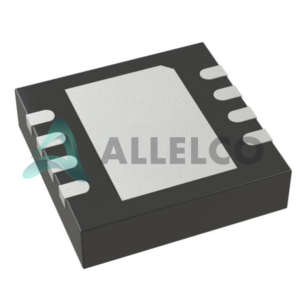
View All

Please refer to the English Version as our Official Version.Return

Europe
France(Français) Germany(Deutsch) Italy(Italia) Russian(русский) Poland(polski) Czech(Čeština) Luxembourg(Lëtzebuergesch) Netherlands(Nederland) Iceland(íslenska) Hungarian(Magyarország) Spain(español) Portugal(Português) Turkey(Türk dili) Bulgaria(Български език) Ukraine(Україна) Greece(Ελλάδα) Israel(עִבְרִית) Sweden(Svenska) Finland(Svenska) Finland(Suomi) Romania(românesc) Moldova(românesc) Slovakia(Slovenská) Denmark(Dansk) Slovenia(Slovenija) Slovenia(Hrvatska) Croatia(Hrvatska) Serbia(Hrvatska) Montenegro(Hrvatska) Bosnia and Herzegovina(Hrvatska) Lithuania(lietuvių) Spain(Português) Switzerland(Deutsch) United Kingdom(English)
Asia/Pacific
Japan(日本語) Korea(한국의) Thailand(ภาษาไทย) Malaysia(Melayu) Singapore(Melayu) Vietnam(Tiếng Việt) Philippines(Pilipino)
Africa, India and Middle East
United Arab Emirates(العربية) Iran(فارسی) Tajikistan(فارسی) India(हिंदी) Madagascar(malaɡasʲ)
South America / Oceania
New Zealand(Maori) Brazil(Português) Angola(Português) Mozambique(Português)
North America
United States(English) Canada(English) Haiti(Ayiti) Mexico(español)
HomeProductsIntegrated Circuits (ICs)PMIC - Voltage Regulators - DC DC Switching RegulatorsLT3502EDC#TRPBF
LT3502EDC#TRPBF Image
Image may be representation.
See specifications for product details.
EXPRESS OPTION
Payment method

LT3502EDC#TRPBF - Analog Devices Inc.

Manufacturer Part Number
LT3502EDC#TRPBF
Manufacturer
Analog Devices, Inc.
Allelco Part Number
32D-LT3502EDC#TRPBF
Warranty
1 Year Allelco Warranty - Find out more
Stock Status:
10,259 pcs available, New & Original
Parts Description
IC REG BUCK ADJ 500MA 8DFN
Package
8-DFN (2x2)
Data sheet
LT3502EDC#TRPBF.pdf
RoHs Status
ROHS3 Compliant
Our certification
In stock: 10259
  • Unit Price: $1.987
  • Subtotal: $0.00

Want a better price?
Add to Cart and Submit RFQ now, we'll contact you immediately.

Quantity Unit Price Ext. Price
1+ $1.987 $1.99
10+ $1.94 $19.40
30+ $1.909 $57.27
100+ $1.878 $187.80
The above prices does not include taxes and freight rates, which will be calculated on the order pages.

Specifications

LT3502EDC#TRPBF Tech Specifications
Analog Devices Inc. - LT3502EDC#TRPBF technical specifications, attributes, parameters and parts with similar specifications to Analog Devices Inc. - LT3502EDC#TRPBF

Product Attribute Attribute Value
Manufacturer Analog Devices, Inc.
Voltage - Output (Min/Fixed) 0.8V
Voltage - Output (Max) 36V
Voltage - Input (Min) 3V
Voltage - Input (Max) 40V
Topology Buck
Synchronous Rectifier No
Supplier Device Package 8-DFN (2x2)
Series -
Package / Case 8-WFDFN Exposed Pad
Product Attribute Attribute Value
Package Tape & Reel (TR)
Output Type Adjustable
Output Configuration Positive
Operating Temperature -40°C ~ 125°C (TJ)
Number of Outputs 1
Mounting Type Surface Mount
Function Step-Down
Frequency - Switching 1.1MHz
Current - Output 500mA
Base Product Number LT3502

Environmental & Export Classifications

ATTRIBUTE DESCRIPTION
RoHs Status ROHS3 Compliant
Moisture Sensitivity Level (MSL) 1 (Unlimited)
REACH Status REACH Unaffected
ECCN EAR99
HTSUS 8542.39.0001

Parts Introduction

LT3502EDC#TRPBF Image
LT3502EDC#TRPBF (1)

Manufacturer Part Number

LT3502EDC#TRPBF

Manufacturer

Analog Devices

Introduction

The LT3502EDC#TRPBF is a step-down (buck) DC-DC switching regulator designed for power management applications, capable of adjusting output voltage and maintaining a stable performance across varying input voltages.

Product Features and Performance

Function: Step-Down

Output Configuration: Positive

Topology: Buck

Output Type: Adjustable

Number of Outputs: 1

Frequency Switching: 1.1MHz

Operating Temperature Range: -40°C to 125°C

Mounting Type: Surface Mount

Package / Case: 8-WFDFN Exposed Pad

Product Advantages

High flexibility with adjustable output voltage ranging from 0.8V to 36V

Wide input voltage range from 3V to 40V suitable for various applications

Compact 8-DFN package for efficient use of PCB space

Key Technical Parameters

Voltage Input (Min): 3V

Voltage Input (Max): 40V

Voltage Output (Min/Fixed): 0.8V

Voltage Output (Max): 36V

Current Output: 500mA

Synchronous Rectifier: No

Quality and Safety Features

Operates efficiently across a wide temperature range of -40°C to 125°C ensuring reliability in harsh environments

Compatibility

Designed for integration with a variety of circuit configurations due to its adjustable output characteristics and compact packaging

Application Areas

Suitable for various power management applications in consumer electronics, industrial systems, and telecommunications

Product Lifecycle

Currently in active production with no indication of discontinuation, ensuring long-term availability and support

Several Key Reasons to Choose This Product

Versatile input and output voltage range suitable for diverse applications

High switching frequency allows for smaller external components, reducing overall design size

Efficient operation over a broad temperature range guarantees performance in varied environmental conditions

Reliable surface mount package ensures durability and ease of integration in complex designs

Frequently Asked Questions(FAQ)

What are the key design considerations when selecting the LT3502EDC#TRPBF for a 500mA buck regulator application with an adjustable output voltage?
The LT3502EDC#TRPBF is suitable for adjustable-output, high-input-voltage buck applications requiring up to 500mA of continuous output current. When designing with this device, engineers must consider the 1.1MHz switching frequency, which enables the use of small external inductors and ceramic capacitors—critical for space-constrained systems. The input voltage range of 3V to 40V supports a broad spectrum of industrial and automotive power rails. However, since it lacks synchronous rectification, efficiency drops at higher input-to-output differentials, particularly above 12V. Output voltage is set using a resistor divider from VOUT to GND, with VFB = 0.8V; thus, R1 and R2 must be chosen to yield the desired VOUT while minimizing power loss and noise sensitivity. Thermal performance in the 8-DFN package should also be evaluated under worst-case load conditions.
How does the LT3502EDC#TRPBF compare to synchronous alternatives like the LT8610 or LTC3637 in terms of efficiency and component count?
The LT3502EDC#TRPBF offers a simpler, lower-cost solution for non-isolated step-down conversion but trades off efficiency due to its asynchronous architecture. In contrast, synchronous regulators such as the LT8610 achieve 10–20% higher efficiency at moderate loads by replacing the Schottky diode with a low-RDS(ON) MOSFET. This results in reduced power dissipation and heat sinking requirements. However, synchronous designs require additional components—typically one extra inductor and control circuitry—which increases board area and BOM cost. For battery-powered or thermally constrained applications, the synchronous advantage may outweigh the simplicity of the LT3502EDC#TRPBF.
Can the LT3502EDC#TRPBF operate reliably in automotive environments, and what precautions are needed for long-term reliability?
Yes, the LT3502EDC#TRPBF operates over a junction temperature range of -40°C to 125°C, meeting basic automotive temperature standards. However, full AEC-Q100 qualification is not specified in the standard datasheet, so designers must verify compliance if used in safety-critical systems. Reliability depends on proper thermal management: the exposed pad must be soldered to a solid ground plane to dissipate heat effectively. Additionally, input transient protection (e.g., TVS diodes) is recommended for automotive load dump scenarios (up to 40V), even though the IC itself supports up to 40V input. Long-term drift in output voltage can occur if feedback resistors are not stable across temperature and time.
What external components are required to configure the LT3502EDC#TRPBF as a fixed 3.3V regulator, and how do they affect stability and transient response?
To set the output to 3.3V, a feedback resistor network is needed with R1 between VOUT and FB, and R2 from FB to GND. Using the formula VOUT = 0.8 × (1 + R1/R2), choosing R2 = 10kΩ yields R1 ≈ 31.5kΩ (standard value: 32.4kΩ). This configuration introduces a small offset (~0.1V), which may be acceptable depending on system tolerance. Stability requires careful selection of output capacitors—low ESR ceramic caps (e.g., X7R ≥10µF) with sufficient RMS ripple current rating. The 1.1MHz switching frequency allows smaller loop compensation than lower-frequency regulators, improving transient response. Nevertheless, PCB layout symmetry around the SW pin remains critical to avoid radiated EMI and ringing.
Is it feasible to parallel multiple LT3502EDC#TRPBF devices to increase total output current beyond 500mA?
Direct paralleling of LT3502EDC#TRPBF units is not recommended without additional balancing circuitry. Since each channel operates independently, current sharing becomes highly imbalanced unless synchronized via external clocks or dedicated master-slave configuration, which the LT3502 does not support natively. Unequal current distribution leads to thermal runaway in the less-loaded unit, especially under light loads or during startup transients. Instead, designers should consider higher-current monolithic solutions such as the LT8614 (1.2A) or discrete multiphase architectures with active current sharing. For most applications, oversizing the inductor and optimizing layout provides more reliable gains than attempting paralleled operation.
How does the LT3502EDC#TRPBF respond to sudden load steps, and what capacitor choices optimize transient recovery?
The LT3502EDC#TRPBF exhibits fast transient response due to its internal error amplifier bandwidth and 1.1MHz switching frequency. Under a 200mA to 500mA load step, output droop typically stays below 100mV if adequate bulk capacitance (≥22µF ceramic) is present at the output. High-ESR bulk capacitors (e.g., polymer) can degrade transient performance, so low-ESR ceramics (X5R/X7R) are preferred. Adding a small feedforward capacitor across R1 improves phase margin slightly but is usually unnecessary. Output voltage overshoot after load removal is minimal (<50mV) due to internal soft-start and controlled shutdown. Careful placement of output capacitors close to the IC minimizes parasitic inductance, which is critical at high switching speeds.
What layout practices are essential to minimize electromagnetic interference (EMI) when using the LT3502EDC#TRPBF?
Minimizing EMI from the LT3502EDC#TRPBF requires a compact, symmetric layout with short traces on the high-current paths. The inductor, input capacitor, and diode (or catch diode) should form a tight loop to reduce radiated magnetic fields. The SW node trace must be routed away from sensitive analog signals, preferably on a separate layer with ground shielding. The exposed pad on the 8-DFN package must be connected to a solid ground plane via multiple vias to ensure low impedance and thermal conductivity. Avoid stubs or right-angle bends on the SW line, as they act as antennas. Proper grounding of the FB pin trace reduces susceptibility to noise coupling into the feedback network.
Can the LT3502EDC#TRPBF be used in a battery-powered IoT device with intermittent operation?
Yes, the LT3502EDC#TRPBF is well-suited for battery-powered IoT applications where the input voltage may vary widely—for example, from a single Li-ion cell (3.3V) up to 12V from a solar panel. Its 90% peak efficiency at light loads (when paired with a suitable diode) helps extend battery life. However, the asynchronous topology results in lower efficiency than synchronous converters below 12V input, so energy consumption during sleep modes must be evaluated. The 1.1MHz frequency keeps inductor size small, beneficial for compact wearable designs. Soft-start functionality prevents inrush current during cold starts, protecting upstream regulators. Always verify that the selected catch diode has adequate reverse recovery characteristics to avoid shoot-through during switching transitions.
How does the LT3502EDC#TRPBF handle startup when powered from a high-impedance source?
Startup behavior depends on the input source’s ability to supply sufficient current during the initial inrush. The LT3502 includes an internal soft-start circuit that ramps the switch current gradually, limiting peak stress on the input supply. If the input source has high series resistance (e.g., long cables or low-capacity batteries), the soft-start duration may cause prolonged startup times or failure to reach regulation. In such cases, adding a small bulk capacitor near the input (≥1µF ceramic) helps buffer transient demand. The EN pin allows external control of turn-on timing, enabling sequencing with other rails. Ensure the EN threshold (typically 1.2V) is compatible with the control logic driving it.
Are there any known limitations in using the LT3502EDC#TRPBF for precision analog subsystems requiring tightly regulated voltages?
While the LT3502EDC#TRPBF can deliver precise output voltages, its suitability for precision analog applications is limited by several factors. The feedback reference is 0.8V, which is less stable than bandgap references in linear regulators, introducing gain errors through resistor tolerances and temperature drift. External resistors with ±0.1% tolerance and low TCR improve accuracy but increase cost. Additionally, switching noise conducted back into the output can couple into sensitive analog circuits unless properly filtered with LC networks or additional post-regulation stages. For systems requiring <1% output accuracy over temperature, a linear post-regulator or dedicated LDO may be preferable despite higher quiescent current.
What impact does input voltage variation have on the LT3502EDC#TRPBF’s output regulation and efficiency?
Input voltage variations significantly affect both regulation and efficiency in the LT3502EDC#TRPBF. At higher input voltages (e.g., 24V to 36V), the duty cycle decreases, reducing conduction losses, but switching losses remain constant due to fixed frequency. Efficiency peaks around mid-range inputs (e.g., 12V to 15V) for a given output. As Vin increases, the diode conduction period lengthens, increasing losses in the external Schottky diode. Below 5V input, the minimum on-time limits achievable output voltage resolution, making sub-1V outputs difficult. Regulation accuracy degrades slightly at very low loads due to comparator offsets, but remains within ±2% under normal operating conditions. Designers should simulate across the full Vin range to identify worst-case thermal and efficiency scenarios.
How does the LT3502EDC#TRPBF compare to the LT3080 in terms of dynamic response and noise performance?
The LT3502EDC#TRPBF and LT3080 serve different purposes: the former is a switching regulator optimized for efficiency and power density, while the latter is a linear regulator designed for ultra-low noise. The LT3502’s 1.1MHz switching inherently generates broadband noise, unsuitable for sensitive analog front-ends, whereas the LT3080 delivers µV-level ripple ideal for precision amplifiers. In terms of dynamic response, the LT3502 responds faster to large load steps due to higher bandwidth control loops, but with greater overshoot and ringing. The LT3080 has slower transient recovery but exceptional line and load regulation. Choosing between them depends on whether efficiency or signal integrity takes precedence.
What are the implications of using the LT3502EDC#TRPBF in a multi-rail system with strict power-up sequencing?
The LT3502EDC#TRPBF does not include built-in sequencing or tracking capabilities. In multi-rail systems, uncontrolled simultaneous power-up can cause excessive inrush current or latch-up in downstream ICs. To implement sequencing, the EN pin can be driven by a supervisory IC or microcontroller GPIO, delaying turn-on relative to other rails. Alternatively, external RC networks on the EN pin can create simple delays, though accuracy depends on component tolerances. Care must be taken to ensure all rails stabilize before enabling loads. Monitoring the FB pin can help detect faults early, but additional monitoring circuits are often required for robust system integration.
Can the LT3502EDC#TRPBF be safely operated near its maximum ratings under pulsed load conditions?
The LT3502EDC#TRPBF is rated for continuous 500mA output current, but pulsed loads exceeding this level are permissible if the average current remains within safe limits and thermal conditions allow. Pulsed operation reduces average power dissipation, lowering junction temperature rise. However, peak currents must not exceed the absolute maximum rating of the switch transistor, typically specified as several amps for short durations. Thermal modeling should account for duty cycle and pulse width to prevent cumulative heating. The soft-start feature also mitigates stress during repeated startups under heavy pulses. Always consult the SOA (Safe Operating Area) graph in the datasheet for specific current vs. time limits under various input and ambient conditions.
How does the choice of external Schottky diode affect overall performance in the LT3502EDC#TRPBF circuit?
The external diode directly impacts efficiency, thermal performance, and reliability in the LT3502EDC#TRPBF. Low-forward-voltage-drop diodes (e.g., 0.3V typical) reduce conduction losses, especially at high currents. Fast-recovery types with low Qrr minimize switching losses and reverse recovery spikes that can damage the main switch or generate EMI. Diodes with adequate surge current capability (e.g., 2A peak) are essential for inductive kickback during turn-off. Package selection (SOT-23 vs. SOD-323) affects thermal resistance and parasitics. Poor diode choice can negate the benefits of the 1.1MHz design, leading to reduced efficiency, increased heat, and potential instability due to ringing on the SW node.
What are the trade-offs involved in selecting a higher switching frequency for similar devices instead of relying on the LT3502EDC#TRPBF’s fixed 1.1MHz?
The LT3502EDC#TRPBF operates at a fixed 1.1MHz, offering a balance between component size and EMI profile. Increasing frequency would reduce inductor and capacitor sizes but raise switching losses, decreasing efficiency and increasing electromagnetic emissions. Lower frequencies improve efficiency but require larger magnetics. Since the LT3502 is not tunable, designers seeking variable frequency operation must choose alternative parts like the LT8610 (with optional synchronization). For most applications, 1.1MHz strikes an optimal compromise. The fixed frequency also simplifies PCB layout and filtering design, reducing risk of resonance issues common with variable-frequency topologies.
Is the LT3502EDC#TRPBF compatible with automated optical inspection (AOI) and high-volume assembly processes?
Yes, the 8-WFDFN package (2x2mm) is fully compatible with standard pick-and-place machines and AOI systems. The exposed pad facilitates solder paste printing and reflow soldering, ensuring good thermal and electrical connection. No special handling procedures are required beyond standard SMT protocols. RoHS3 compliance and MSL 1 classification mean it can be stored indefinitely and processed without baking. However, the small footprint demands precise stencil design and alignment to avoid tombstoning or insufficient solder joints. Automated testing of the FB pin during production helps catch calibration drift early. Overall, the LT3502EDC#TRPBF integrates seamlessly into high-volume manufacturing workflows.
What diagnostic features does the LT3502EDC#TRPBF offer for system-level fault detection?
The LT3502EDC#TRPBF includes limited built-in diagnostics. The EN pin allows external control and status monitoring, enabling software-based enable/disable logic. Internal soft-start prevents overcurrent during startup, protecting both the IC and upstream supplies. However, there is no open-circuit detection, overtemperature lockout reporting, or fault flag output. Overvoltage protection is passive, relying on the feedback loop to shut down if VOUT exceeds 36V. For robust fault diagnosis, designers often add external comparators to monitor FB and VIN, triggering reset lines or logging events. Without additional circuitry, real-time health monitoring is minimal, so system-level safeguards must complement the IC’s inherent protections.

Parts with Similar Specifications

The three parts on the right have similar specifications to Analog Devices Inc. LT3502EDC#TRPBF

Product Attribute LT3502EDC#TRMPBF LT3502IDC#TRMPBF LT3502IDC#TRPBF LT3502AIDC#TRPBF
Part Number LT3502EDC#TRMPBF LT3502IDC#TRMPBF LT3502IDC#TRPBF LT3502AIDC#TRPBF
Manufacturer Analog Devices Inc. Analog Devices Inc. Analog Devices Inc. Analog Devices Inc.
Mounting Type - Surface Mount Through Hole Surface Mount
Base Product Number - DAC34H84 MAX500 ADS62P42
Voltage - Output (Min/Fixed) - - - -
Series - - - -
Package / Case - 196-LFBGA 16-DIP (0.300', 7.62mm) 64-VFQFN Exposed Pad
Operating Temperature - -40°C ~ 85°C 0°C ~ 70°C -40°C ~ 85°C
Synchronous Rectifier - - - -
Output Type - Current - Unbuffered Voltage - Buffered -
Package - Tape & Reel (TR) Tube Tape & Reel (TR)
Voltage - Input (Max) - - - -
Supplier Device Package - 196-NFBGA (12x12) 16-PDIP 64-VQFN (9x9)
Output Configuration - - - -
Topology - - - -
Voltage - Input (Min) - - - -
Current - Output - - - -
Voltage - Output (Max) - - - -
Frequency - Switching - - - -
Number of Outputs - - - -
Function - - - -

LT3502EDC#TRPBF Datasheet PDF

Download LT3502EDC#TRPBF pdf datasheets and Analog Devices Inc. documentation for LT3502EDC#TRPBF - Analog Devices Inc..

Datasheets
LT3502(A) Datasheet.pdf LTpowerCAD II Quick Start Guide.pdf LTpowerCAD II User Guide.pdf
Environmental Information
Material Declaration LT3502EDC#TRPBF.pdf
Other Related Documents
Tape and Reel Packaging.pdf

Customer Reviews

Evaluation: 10 Articles

  • Dani***alkerTech
    Jun 1, 2026

    Product works, but setup took more effort than expected. Once configured the MCU ran reliably, although documentation support felt older compared with newer platforms. Fine for maintenance projects.

  • Yuki***aka88
    May 26, 2026

    信号通信プロジェクトでこのRS-485トランシーバーを使用しました。設置は簡単で、長距離ケーブルでも通信は安定していました。消費電力も、以前使用していたものより低くなっています。

  • Stev***aker
    May 20, 2026

    Solid diode for power rectification. Works well in switching circuits.

  • Bran***Lewis
    May 11, 2026

    Compact FPGA with good performance. Suitable for basic signal processing tasks.

  • Oliv***arris
    May 7, 2026

    Reliable I/O expander. Works well in embedded control applications.

  • Jess***Jones
    Apr 17, 2026

    It offers good value for the price, and the specifications match the description. I’ve been using it for two days with no issues, and I’ll definitely buy it again if I need it in the future.

  • Mich***Smith
    Apr 17, 2026

    Shipping was on time, the component pins are neatly aligned, and I tested 10 of them with a multimeter—all readings were within the specified range. Highly recommended.

  • Aman***arris
    Apr 3, 2026

    It was great—the entire process, from placing the order to receiving the package, went very smoothly. The components were consistent, the price was fair, and I had a very pleasant shopping experience.

  • Mike***nch
    Apr 3, 2026

    Better than expected! The resistance and capacitance readings were spot-on, and it passed the test on the first try. The service was reliable, and the packaging was thoughtful—I highly recommend it.

  • Daic***K.
    Mar 23, 2026

    Very good. No issue after long time testing.

Write a Review

Your Email address will not be published.

Shipment

Delivery Time

In-stock items can be shipped within 24 hours. Some parts will be arranged for delivery within 1-2 days from the date all items arrive at our warehouse. And Allelco ships order once a day at about 17:00, except Sunday. Once the goods are shipped, the estimated delivery time depends on the shipping methods and Delivery destination. The table below shows are the logistic time for some common countries.

Delivery Cost

  1. Use your express account for shipment if you have one.
  2. Use our account for the shipment. Refer to the table below for the approximate charges.
(Different time frame / countries / package size has different price.)

Delivery Method

  1. Global Common Shipment by DHL / UPS / FedEx / TNT / EMS / SF we support.
  2. Others more shipping ways, please get in touch with your customer manager.

Common Countries Logistic Time Reference
Region Country Logistic Time(Day)
America United States 5
Brazil 7
Europe Germany 5
United Kingdom 4
Italy 5
Oceania Australia 6
New Zealand 5
Asia India 4
Japan 4
Middle East Israel 6
DHL & FedEx Shipment Charges Reference
Shipment charges(KG) Reference DHL(USD$)
0.00kg-1.00kg USD$30.00 - USD$60.00
1.00kg-2.00kg USD$40.00 - USD$80.00
2.00kg-3.00kg USD$50.00 - USD$100.00
Note:
The above table is for reference only. There may have some data bias for the uncontrollable factors.
Contact us if you have any questions.
  • QC (Quality Warranty)
  • Payment Support
  • Packaging
  • Certifications & Memberships

QC (Quality Warranty)

Allelco is committed to exceeding customer expectations through customer service excellence, order accuracy, and on-time delivery.
This is achieved through our commitment to the continual improvement of our processes, services, and products.


Strict quality inspection builds a solid foundation for electronic component quality.
  1. Visual inspection
  2. Performance testing and reliability verification
  3. Standardized full-process testing
  4. Precise control of every parameter
We eliminate defective components and ensure the stable operation of electronic devices through professional quality standards.

Payment Support

The payment method can be chosen from the methods shown below: Wire Transfer (T/T, Bank Transfer), Western Union, Credit card, PayPal.
  • HKBea
  • Paypal
  • MasterCard
  • Western-Union
  • VISA
Stable Delivery, Sincere Partnership — Your Faithful Supply Chain Partner
  • Efficient Supply Management
  • Cost-Saving Procurement
  • Fast Sourcing & Delivery
Contact us if you have any questions.

Packaging

Electrostatic Discharge Protection and Handling

All electrostatic-sensitive components are handled in accordance with electrostatic discharge control procedures. The products are hermetically sealed in anti-static safe packaging to prevent electrostatic damage. Appropriate labeling is also applied for identification and traceability. This ensures product integrity during storage, handling and transportation.


ESD

Certifications & Memberships

Third-party certified, strict quality control. Our certification
  • ISO 9001: 2015
  • ISO 13485: 2016
  • ISO 14001: 2015
  • ISO 28000: 2007
  • ISO 45001: 2018
  • GB/T 27922-2011
  • SMTA
  • IPC
  • ESD
  • PSMA
LT3502EDC#TRPBF Image

LT3502EDC#TRPBF

Analog Devices Inc.
32D-LT3502EDC#TRPBF

Want a better price? Add to Cart and Submit RFQ now, we'll contact you immediately.

0 RFQ
Shopping cart (0 Items)
It is empty.
Compare List (0 Items)
It is empty.
Feedback

Your feedback matters! At Allelco, we value the user experience and strive to improve it constantly.
Please share your comments with us via our feedback form, and we'll respond promptly.
Thank you for choosing Allelco.

Subject
E-mail
Comments
Captcha
Drag or click to upload file
Upload File
types: .xls, .xlsx, .doc, .docx, .jpg, .png and .pdf.
Max file size: 10MB