View All

Please refer to the English Version as our Official Version.Return

Europe
France(Français) Germany(Deutsch) Italy(Italia) Russian(русский) Poland(polski) Czech(Čeština) Luxembourg(Lëtzebuergesch) Netherlands(Nederland) Iceland(íslenska) Hungarian(Magyarország) Spain(español) Portugal(Português) Turkey(Türk dili) Bulgaria(Български език) Ukraine(Україна) Greece(Ελλάδα) Israel(עִבְרִית) Sweden(Svenska) Finland(Svenska) Finland(Suomi) Romania(românesc) Moldova(românesc) Slovakia(Slovenská) Denmark(Dansk) Slovenia(Slovenija) Slovenia(Hrvatska) Croatia(Hrvatska) Serbia(Hrvatska) Montenegro(Hrvatska) Bosnia and Herzegovina(Hrvatska) Lithuania(lietuvių) Spain(Português) Switzerland(Deutsch) United Kingdom(English)
Asia/Pacific
Japan(日本語) Korea(한국의) Thailand(ภาษาไทย) Malaysia(Melayu) Singapore(Melayu) Vietnam(Tiếng Việt) Philippines(Pilipino)
Africa, India and Middle East
United Arab Emirates(العربية) Iran(فارسی) Tajikistan(فارسی) India(हिंदी) Madagascar(malaɡasʲ)
South America / Oceania
New Zealand(Maori) Brazil(Português) Angola(Português) Mozambique(Português)
North America
United States(English) Canada(English) Haiti(Ayiti) Mexico(español)
HomeProductsIntegrated Circuits (ICs)Embedded - FPGAs (Field Programmable Gate Array)XC7A200T-2FBG484I
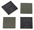
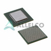
XC7A200T-2FBG484I Image
Image may be representation.
See specifications for product details.
EXPRESS OPTION
Payment method

XC7A200T-2FBG484I - AMD

Manufacturer Part Number
XC7A200T-2FBG484I
Manufacturer
AMD Xilinx
Allelco Part Number
32D-XC7A200T-2FBG484I
Warranty
1 Year Allelco Warranty - Find out more
Stock Status:
14,971 pcs available, New & Original
Parts Description
IC FPGA 285 I/O 484FCBGA
Package
484-FCBGA (23x23)
Data sheet
XC7A200T-2FBG48.pdf
RoHs Status
ROHS3 Compliant
Our certification
In stock: 14971
  • Unit Price: $38.70
  • Subtotal: $0.00

Want a better price?
Add to Cart and Submit RFQ now, we'll contact you immediately.

Quantity Unit Price Ext. Price
1+ $38.70 $38.70
3+ $36.77 $110.31
30+ $35.11 $1,053.30
The above prices does not include taxes and freight rates, which will be calculated on the order pages.

Specifications

XC7A200T-2FBG484I Tech Specifications
AMD - XC7A200T-2FBG484I technical specifications, attributes, parameters and parts with similar specifications to AMD - XC7A200T-2FBG484I

Product Attribute Attribute Value
Manufacturer AMD Xilinx
Voltage - Supply 0.95V ~ 1.05V
Total RAM Bits 13455360
Supplier Device Package 484-FCBGA (23x23)
Series Artix-7
Package / Case 484-BBGA, FCBGA
Package Tray
Product Attribute Attribute Value
Operating Temperature -40°C ~ 100°C (TJ)
Number of Logic Elements/Cells 215360
Number of LABs/CLBs 16825
Number of I/O 285
Mounting Type Surface Mount
Base Product Number XC7A200

Environmental & Export Classifications

ATTRIBUTE DESCRIPTION
RoHs Status ROHS3 Compliant
Moisture Sensitivity Level (MSL) 4 (72 Hours)
REACH Status REACH Unaffected
ECCN 3A991D
HTSUS 8542.39.0001

Parts Introduction

XC7A200T-2FBG484I Image
XC7A200T-2FBG484I (1)

Manufacturer Part Number

XC7A200T-2FBG484I

Manufacturer

Xilinx

XC7A200T-2FBG484I Image
XC7A200T-2FBG484I (2)

Introduction

The XC7A200T-2FBG484I is part of the Artix-7 family of FPGAs, offering advanced digital processing capabilities suitable for a wide range of applications.

Product Features and Performance

High-density integration with 215360 logic elements and 16825 LABs/CLBs

Extensive memory resources with 13455360 total RAM bits

Supports up to 285 I/O pins for flexible connectivity

Low power supply requirements (0.95V ~ 1.05V)

Robust operating temperature range from -40°C to 100°C

Product Advantages

Superior logic density for complex digital systems

Ample memory for advanced data buffering and manipulation

Highly adaptable I/O configuration

Low power consumption for energy-efficient designs

Suitable for harsh environments with extended temperature range

XC7A200T-2FBG484I Image
XC7A200T-2FBG484I (3)

Key Technical Parameters

Number of LABs/CLBs: 16825

Number of Logic Elements/Cells: 215360

Total RAM Bits: 13455360

Number of I/O: 285

Voltage Supply: 0.95V ~ 1.05V

Operating Temperature: -40°C ~ 100°C

Quality and Safety Features

Reliable surface mount package (484-FCBGA)

High thermal tolerance ensuring stable operation under thermal stress

Compatibility

Compatible with multiple standard voltage and logic level systems due to flexible I/O voltage support

XC7A200T-2FBG484I Image
XC7A200T-2FBG484I (4)

Application Areas

High-speed communications equipment

Digital signal processing

Aerospace and defense electronics

Industrial automation and control systems

Product Lifecycle

Status: Active

Not nearing discontinuation, with ongoing support and availability

Several Key Reasons to Choose This Product

Exceptional integration capacity with substantial logic and memory resources

Resilient to infrastructural challenges due to broad operating temperature range and low power needs

Suitable for future-proof designs in advanced electronic systems

Reliable manufacturer with proven expertise in FPGA technology

Frequently Asked Questions(FAQ)

How does the XC7A200T-2FBG484I's power efficiency compare to other FPGA families when targeting low-voltage embedded designs requiring over 200K logic elements?
The XC7A200T-2FBG484I operates across a tightly regulated supply range of 0.95V to 1.05V, which is characteristic of advanced CMOS scaling in the Artix-7 family. This enables significantly lower dynamic and static power consumption compared to older-generation FPGAs such as Spartan-6 or Virtex-5 devices at equivalent logic densities. When designing for systems where power budget is constrained—such as industrial control units or battery-powered instrumentation—the reduced voltage rail minimizes switching losses per logic element. With 215,360 logic cells and 16,825 LABs, the device delivers high logic density without requiring aggressive clock gating or architectural compromises, making it more power-efficient than larger Stratix or Kintex parts that would otherwise exceed thermal or current limits.
What are the key trade-offs between using the XC7A200T-2FBG484I versus discrete logic solutions in high-channel-count serial communication applications?
In high-channel-count serial communication designs—such as those using multiple SERDES lanes—the XC7A200T-2FBG484I offers substantial integration benefits over discrete logic implementations. While discrete solutions may reduce upfront cost for small channel counts, they increase board area, routing complexity, and susceptibility to skew and jitter. The XC7A200T integrates hardened GTX transceivers (typically up to 6.6 Gbps), reducing reliance on external PHY chips and simplifying timing closure. However, this comes with higher unit cost and longer bring-up time due to FPGA configuration and validation. For applications requiring more than 8–10 high-speed serial channels, the XC7A200T becomes preferable despite its premium pricing over pure ASIC or discrete logic alternatives.
Can the XC7A200T-2FBG484I be used in safety-critical systems that require functional safety certification?
The XC7A200T-2FBG484I itself is not inherently certified for functional safety standards such as IEC 61508 or ISO 26262. While it supports design techniques like triple modular redundancy (TMR) and error-correcting code (ECC) memory via internal block RAM, achieving certification requires additional measures including hardware fault injection testing, diagnostic coverage analysis, and third-party assessment. Engineers considering safety-critical deployment must supplement the FPGA with external watchdog circuits, redundant power supplies, and rigorous lifecycle management. AMD (formerly Xilinx) provides limited support documentation for safety-oriented use cases, but full certification remains the responsibility of the system integrator.
What considerations apply when selecting bypass capacitors for the XC7A200T-2FBG484I’s core voltage rails in a space-constrained PCB layout?
Given the tight voltage tolerance of 0.95V to 1.05V, decoupling for the XC7A200T-2FBG484I demands careful attention to transient response and loop inductance. Due to its 484-pin FCBGA package with fine-pitch BGA, mounting bypass capacitors close to VCCINT pins minimizes parasitic inductance. A typical design uses a combination of high-frequency ceramic capacitors (e.g., 100 nF X7R 0402) placed within 1–2 mm of the package and bulk capacitance (e.g., 10 µF polymer) on each power plane segment. The MSL 4 classification indicates sensitivity to moisture, so assembly processes must adhere to JEDEC J-STD-033 guidelines to avoid delamination during reflow, especially when placing small-value MLCCs near high-density BGA areas.
How does the operating temperature range of the XC7A200T-2FBG484I impact its reliability in automotive edge-node deployments?
The XC7A200T-2FBG484I supports junction temperatures from -40°C to +100°C, which aligns with commercial and industrial environments but falls short of the -40°C to +125°C required by many automotive grades. In automotive edge nodes—such as camera preprocessing units or sensor fusion hubs—prolonged exposure to ambient temperatures above 85°C may push the die temperature beyond specification during peak power dissipation. Thermal modeling must account for airflow, heatsinking, and concurrent activity across all 285 I/Os and internal blocks. Without automotive qualification, derating the maximum junction temperature to 90°C or below is advisable to ensure long-term reliability under real-world conditions.
What are the implications of the XC7A200T-2FBG484I’s 134,553,60 total RAM bits for implementing deep packet buffers in networking equipment?
With 134,553,60 bits of distributed and block RAM, the XC7A200T-2FBG484I can support moderately sized packet buffers in line-rate processing pipelines. For example, a single 10 Gbps port buffering 100 μs of traffic requires approximately 12.5 MB of storage. The XC7A200T provides only about 16.8 MB total, meaning multiple ports would exhaust available memory quickly unless compressed or shared intelligently. Designers must therefore optimize buffer allocation, prioritize critical queues, or offload overflow to external DDR3/LPDDR2 memory. This constraint makes the part suitable for mid-range switches or routers but less ideal for high-performance systems requiring terabit-scale buffering.
How should signal integrity be managed when routing user-defined I/O adjacent to transceiver lanes on the XC7A200T-2FBG484I?
Adjacent to the GTX transceiver banks, the XC7A200T-2FBG484I exposes sensitive analog reference circuits and high-speed differential pairs that demand strict signal integrity practices. User I/O routed nearby must maintain minimum separation from transceiver traces to avoid crosstalk, especially during TX/RX transitions at 6.6 Gbps. Differential pair lengths should match within ±5 mils, and impedance controlled to 100 Ω for LVDS and 50 Ω for single-ended signals. Additionally, power delivery to transceiver cores (separate from VCCINT) must remain stable; noise coupling into these domains can degrade eye diagram performance. Layer stackup planning and pre-layout simulation using IBIS models are strongly recommended before committing to physical implementation.
What role does the Moisture Sensitivity Level (MSL) 4 classification play in manufacturing yield and reliability for the XC7A200T-2FBG484I?
The MSL 4 rating for the XC7A200T-2FBG484I signifies a moisture sensitivity level of 72 hours at 30°C/60% RH before assembly. This classification mandates controlled humidity storage and bake-out procedures prior to solder reflow if the device has been exposed beyond the floor life window. Failure to follow IPC/JEDEC J-STD-033 guidelines increases the risk of popcorning—cracking of the plastic mold compound upon rapid heating—which could lead to delamination and eventual electrical failure. Manufacturers must track lot history, implement humidity indicator cards, and schedule baking for opened trays. This requirement adds process overhead but is essential for maintaining yield in high-volume production environments.
How does the XC7A200T-2FBG484I’s configuration interface compare to newer FPGA families in terms of security and reconfigurability?
Unlike modern FPGAs supporting AES-256 encryption via onboard configuration flash, the XC7A200T-2FBG484I relies on basic SPI or SelectMAP interfaces without hardware-protected bitstream decryption. This makes it vulnerable to reverse engineering and unauthorized firmware extraction unless supplemented with external secure elements. Additionally, partial reconfiguration capabilities are limited compared to UltraScale+ or Versal architectures, restricting dynamic runtime updates. For applications demanding field-updatable logic or secure boot, engineers may need to pair the XC7A200T with an external trusted platform module (TPM) or migrate to a later-generation device offering native hardening features.
What design constraints arise from the XC7A200T-2FBG484I’s 285 I/O count when interfacing with legacy parallel buses like PCI or ISA?
The XC7A200T-2FBG484I’s 285 general-purpose I/Os are flexible but lack dedicated hard macros for legacy interfaces such as PCI or ISA. Implementing these buses in software requires significant logic resources and precise timing control, increasing latency and reducing throughput. Moreover, legacy signaling levels (e.g., TTL, LVTTL) must be translated using level shifters or internal I/O bank regulators, consuming additional power and board space. Given the complexity, most designers opt for modern serial protocols instead. If legacy compatibility is mandatory, resource estimation must include not just I/O allocation but also timing closure effort and potential reduction in usable logic capacity.
Why might the XC7A200T-2FBG484I be preferred over smaller Artix-7 variants despite its higher pin count and cost?
Although smaller Artix-7 devices exist (e.g., XC7A35T, XC7A50T), the XC7A200T-2FBG484I offers scalability for designs anticipating future feature expansion or requiring deterministic performance at scale. Its 215K logic elements provide headroom for algorithmic refinement, while abundant block RAM and DSP slices support complex digital filters or matrix operations without external memory. The larger package also facilitates better thermal dissipation and easier probing during debug. For production volumes exceeding 10k units, the non-recurring engineering (NRE) savings of avoiding multiple device migrations justify the higher per-unit cost in medium-to-high complexity systems.
How does the XC7A200T-2FBG484I handle clock domain crossing (CDC) in asynchronous multi-sampling systems?
The XC7A200T-2FBG484I includes built-in synchronization primitives and CDC detection tools in Vivado, but proper CDC handling still depends on disciplined design methodology. Crossing clock domains without synchronizers risks metastability, which can corrupt data and propagate through critical paths. Best practice involves using double-flop synchronizers for single-bit signals and FIFOs or handshake protocols for wider words. Given its high number of global clock buffers and regional clock networks, the device supports efficient distribution of multiple asynchronous clocks, but timing analysis must explicitly check for CDC violations during synthesis. Failure to do so may result in intermittent failures unobservable during simulation.

Parts with Similar Specifications

The three parts on the right have similar specifications to AMD XC7A200T-2FBG484I

Product Attribute XC7A200T-2FB484I XC7A200T-2FBG484C XC7A200T-1SBG484I XC7A200T-1SBG484C
Part Number XC7A200T-2FB484I XC7A200T-2FBG484C XC7A200T-1SBG484I XC7A200T-1SBG484C
Manufacturer AMD AMD AMD AMD
Number of I/O - - - -
Package - Tape & Reel (TR) Tube Tape & Reel (TR)
Operating Temperature - -40°C ~ 85°C 0°C ~ 70°C -40°C ~ 85°C
Total RAM Bits - - - -
Package / Case - 196-LFBGA 16-DIP (0.300', 7.62mm) 64-VFQFN Exposed Pad
Base Product Number - DAC34H84 MAX500 ADS62P42
Number of LABs/CLBs - - - -
Voltage - Supply - - - -
Mounting Type - Surface Mount Through Hole Surface Mount
Series - - - -
Supplier Device Package - 196-NFBGA (12x12) 16-PDIP 64-VQFN (9x9)
Number of Logic Elements/Cells - - - -

XC7A200T-2FBG484I Datasheet PDF

Download XC7A200T-2FBG484I pdf datasheets and AMD documentation for XC7A200T-2FBG484I - AMD.

Datasheets
Artix-7 FPGAs Brief.pdf
PCN Design/Specification
Cross-Ship Lead-Free Notice 31/Oct/2016.pdf Mult Dev Material Chg 16/Dec/2019.pdf
Environmental Information
Xilinx REACH211 Cert.pdf

Customer Reviews

Evaluation: 10 Articles

  • ECUb***h
    Sep 22, 2026

    Used for repair of an older automotive ECU. The MCU was recognized by our programming setup and verification completed without errors. The repaired board now starts and communicates normally.

  • RS48***ieldTech
    Sep 16, 2026

    Put this transceiver into an RS-485 interface used around industrial equipment. Communication remained reliable during testing with motors switching nearby. Good result for the replacement board.

  • Logi***b_Chris
    Sep 8, 2026

    Purchased for a Cyclone III development project. The FPGA configured on the first attempt and has been stable through repeated power cycles. No problems with the I/O we are using.

  • Circ***FixerTom
    Sep 2, 2026

    Used this rectifier in a high-current power supply repair. Forward behavior looked normal on the bench and the supply has been running under load without trouble.

  • Retr***UWorks
    Aug 31, 2026

    Needed the exact ST10F269Z2Q6 for servicing an older control unit. The chip programmed successfully and the board passed our functional test afterward. Much easier than redesigning around a newer MCU.

  • Andr***PCBLab
    Aug 28, 2026

    I needed this ADC for an older data acquisition board. Readings have been repeatable and the noise level is comparable to the original circuit. Happy with the purchase.

  • Leat***O'Keefe
    Aug 20, 2026

    one of my hobbies is skydiving. and when i'm skydiving this works great.

  • Ilen***
    Aug 20, 2026

    This product works considerably well. It secretly improves my basketball by a lot.

  • Indu***ialPower
    Aug 17, 2026

    Installed this IGBT module in a power conversion cabinet. Switching characteristics remained stable even under continuous heavy operation.

  • Nikh***ech
    Aug 13, 2026

    Great low-power MCU for portable equipment. Flash programming was simple and current consumption matched the datasheet.

Write a Review

Your Email address will not be published.

Shipment

Delivery Time

In-stock items can be shipped within 24 hours. Some parts will be arranged for delivery within 1-2 days from the date all items arrive at our warehouse. And Allelco ships order once a day at about 17:00, except Sunday. Once the goods are shipped, the estimated delivery time depends on the shipping methods and Delivery destination. The table below shows are the logistic time for some common countries.

Delivery Cost

  1. Use your express account for shipment if you have one.
  2. Use our account for the shipment. Refer to the table below for the approximate charges.
(Different time frame / countries / package size has different price.)

Delivery Method

  1. Global Common Shipment by DHL / UPS / FedEx / TNT / EMS / SF we support.
  2. Others more shipping ways, please get in touch with your customer manager.

Common Countries Logistic Time Reference
Region Country Logistic Time(Day)
America United States 5
Brazil 7
Europe Germany 5
United Kingdom 4
Italy 5
Oceania Australia 6
New Zealand 5
Asia India 4
Japan 4
Middle East Israel 6
DHL & FedEx Shipment Charges Reference
Shipment charges(KG) Reference DHL(USD$)
0.00kg-1.00kg USD$30.00 - USD$60.00
1.00kg-2.00kg USD$40.00 - USD$80.00
2.00kg-3.00kg USD$50.00 - USD$100.00
Note:
The above table is for reference only. There may have some data bias for the uncontrollable factors.
Contact us if you have any questions.
  • QC (Quality Warranty)
  • Payment Support
  • Packaging
  • Certifications & Memberships

QC (Quality Warranty)

Allelco is committed to exceeding customer expectations through customer service excellence, order accuracy, and on-time delivery.
This is achieved through our commitment to the continual improvement of our processes, services, and products.


Strict quality inspection builds a solid foundation for electronic component quality.
  1. Visual inspection
  2. Performance testing and reliability verification
  3. Standardized full-process testing
  4. Precise control of every parameter
We eliminate defective components and ensure the stable operation of electronic devices through professional quality standards.

Payment Support

The payment method can be chosen from the methods shown below: Wire Transfer (T/T, Bank Transfer), Western Union, Credit card, PayPal.
  • HKBea
  • Paypal
  • MasterCard
  • Western-Union
  • VISA
Stable Delivery, Sincere Partnership — Your Faithful Supply Chain Partner
  • Efficient Supply Management
  • Cost-Saving Procurement
  • Fast Sourcing & Delivery
Contact us if you have any questions.

Packaging

Electrostatic Discharge Protection and Handling

All electrostatic-sensitive components are handled in accordance with electrostatic discharge control procedures. The products are hermetically sealed in anti-static safe packaging to prevent electrostatic damage. Appropriate labeling is also applied for identification and traceability. This ensures product integrity during storage, handling and transportation.


ESD

Certifications & Memberships

Third-party certified, strict quality control. Our certification
  • ISO 9001: 2015
  • ISO 13485: 2016
  • ISO 14001: 2015
  • ISO 28000: 2007
  • ISO 45001: 2018
  • GB/T 27922-2011
  • SMTA
  • IPC
  • ESD
  • PSMA
XC7A200T-2FBG484I Image

XC7A200T-2FBG484I

AMD
32D-XC7A200T-2FBG484I

Want a better price? Add to Cart and Submit RFQ now, we'll contact you immediately.

0 RFQ
Shopping cart (0 Items)
It is empty.
Compare List (0 Items)
It is empty.
Feedback

Your feedback matters! At Allelco, we value the user experience and strive to improve it constantly.
Please share your comments with us via our feedback form, and we'll respond promptly.
Thank you for choosing Allelco.

Subject
E-mail
Comments
Captcha
Drag or click to upload file
Upload File
types: .xls, .xlsx, .doc, .docx, .jpg, .png and .pdf.
Max file size: 10MB