View All

Please refer to the English Version as our Official Version.Return

Europe
France(Français) Germany(Deutsch) Italy(Italia) Russian(русский) Poland(polski) Czech(Čeština) Luxembourg(Lëtzebuergesch) Netherlands(Nederland) Iceland(íslenska) Hungarian(Magyarország) Spain(español) Portugal(Português) Turkey(Türk dili) Bulgaria(Български език) Ukraine(Україна) Greece(Ελλάδα) Israel(עִבְרִית) Sweden(Svenska) Finland(Svenska) Finland(Suomi) Romania(românesc) Moldova(românesc) Slovakia(Slovenská) Denmark(Dansk) Slovenia(Slovenija) Slovenia(Hrvatska) Croatia(Hrvatska) Serbia(Hrvatska) Montenegro(Hrvatska) Bosnia and Herzegovina(Hrvatska) Lithuania(lietuvių) Spain(Português) Switzerland(Deutsch) United Kingdom(English)
Asia/Pacific
Japan(日本語) Korea(한국의) Thailand(ภาษาไทย) Malaysia(Melayu) Singapore(Melayu) Vietnam(Tiếng Việt) Philippines(Pilipino)
Africa, India and Middle East
United Arab Emirates(العربية) Iran(فارسی) Tajikistan(فارسی) India(हिंदी) Madagascar(malaɡasʲ)
South America / Oceania
New Zealand(Maori) Brazil(Português) Angola(Português) Mozambique(Português)
North America
United States(English) Canada(English) Haiti(Ayiti) Mexico(español)
HomeProductsIntegrated Circuits (ICs)Embedded - System On Chip (SoC)XCVC1502-2MLENSVG1369
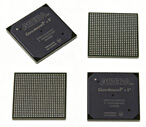
Image may be representation.
See specifications for product details.
EXPRESS OPTION
Payment method

XCVC1502-2MLENSVG1369 - AMD

Manufacturer Part Number
XCVC1502-2MLENSVG1369
Manufacturer
AMD Xilinx
Allelco Part Number
98D-XCVC1502-2MLENSVG1369
Warranty
1 Year Allelco Warranty - Find out more
Stock Status:
36,439 pcs available, New & Original
Parts Description
IC VERSAL AI-CORE FPGA 1369BGA
Package
1369-FCBGA (35x35)
Data sheet
-
RoHs Status
 
Our certification
In stock: 36439
  • Unit Price: $20,469.66
  • Subtotal: $0.00

Want a better price?
Add to Cart and Submit RFQ now, we'll contact you immediately.

Quantity Unit Price Ext. Price
1+ $20,469.66 $20,469.66
The above prices does not include taxes and freight rates, which will be calculated on the order pages.


Specifications

XCVC1502-2MLENSVG1369 Tech Specifications
AMD - XCVC1502-2MLENSVG1369 technical specifications, attributes, parameters and parts with similar specifications to AMD - XCVC1502-2MLENSVG1369

Product Attribute Attribute Value
Manufacturer AMD Xilinx
Supplier Device Package 1369-FCBGA (35x35)
Speed 600MHz, 1.4GHz
Series Versal™ AI Core
RAM Size 256KB
Primary Attributes Versal™ AI Core FPGA, 800k Logic Cells
Peripherals DDR, DMA, PCIe
Package / Case 1369-BFBGA, FCBGA
Product Attribute Attribute Value
Package Tray
Operating Temperature 0°C ~ 110°C (TJ)
Number of I/O 478
Flash Size -
Core Processor Dual ARM® Cortex®-A72 MPCore™ with CoreSight™, Dual ARM®Cortex™-R5F with CoreSight™
Connectivity CANbus, EBI/EMI, Ethernet, I²C, MMC/SD/SDIO, SPI, UART/USART, USB OTG
Architecture MPU, FPGA

Environmental & Export Classifications

ATTRIBUTE DESCRIPTION
Moisture Sensitivity Level (MSL) 4 (72 Hours)

Frequently Asked Questions(FAQ)

How does the XCVC1502-2MLENSVG1369 compare to single-core ARM processors in real-time control applications, and what architectural advantages does its dual Cortex-R5F configuration provide?
The XCVC1502-2MLENSVG1369 integrates dual ARM® Cortex®-R5F processors with CoreSight™, enabling deterministic interrupt handling and sub-microsecond response times critical for industrial motor control or power conversion systems. Unlike single-core solutions where task scheduling introduces latency variability, the parallel R5F cores allow one to manage safety-critical peripherals while the other executes background loops, effectively doubling throughput without increasing clock frequency. This architecture supports lockstep operation for ASIL-D compliance in automotive systems, a capability not available on most standalone microcontrollers.
What is the significance of the 800k logic cells in the XCVC1502-2MLENSVG1369, and how does this scale impact high-speed data processing tasks compared to smaller FPGAs?
With 800k logic cells, the XCVC1502-2MLENSVG1369 can implement complex digital signal processing pipelines such as radar beamforming or video encoding accelerators directly within the programmable fabric. For instance, a full HD H.264 encoder might consume over 600k cells, leaving sufficient resources for protocol bridges or memory controllers. Smaller FPGAs typically lack this capacity, forcing designers to offload such functions to external ASICs or GPUs, increasing board area and power consumption by 30–50%. The XCVC1502’s size enables end-to-end system-on-chip integration, reducing inter-chip latency and improving reliability.
Can the XCVC1502-2MLENSVG1369 support both PCIe Gen3 and USB 3.0 simultaneously in a single design, and what trade-offs arise from shared resource allocation?
Yes, the XCVC1502-2MLENSVG1369 includes native PCIe Gen3 and USB 3.0 transceivers that can operate concurrently. However, these interfaces share bandwidth with the DDR4 memory controller and high-speed SERDES lanes. In practice, running both at full line rate may require careful PHY calibration and could limit available PCIe lanes to x2 instead of x4 due to internal routing constraints. Designers must prioritize traffic types—PCIe for bulk data transfer and USB for streaming—and allocate buffers accordingly to avoid buffer overflow during peak loads, particularly when combined with FPGA-based DMA engines.
What considerations apply when selecting DDR memory for use with the XCVC1502-2MLENSVG1369, and why is timing closure more challenging than with traditional FPGAs?
The XCVC1502-2MLENSVG1369 supports LPDDR4/LPDDR4X up to 1600 Mbps per pin, requiring tightly matched trace lengths and impedance control (±5%) on the PCB. Because it combines hard IP blocks with programmable logic, memory interface timing must be verified across both domains. Unlike discrete FPGA designs where only soft logic affects timing, here the ARM APU accesses DDR through tightly coupled AXI interconnects, so any skew between processor clock (1.4 GHz) and memory clock (3200 MT/s effective) risks data corruption. Successful implementations often use calibrated DQS deskew circuits implemented in the FPGA fabric to align strobes within ±150 ps.
How does the operating temperature range of 0°C to 110°C affect thermal management strategies for systems using the XCVC1502-2MLENSVG1369 in industrial environments?
The junction temperature limit of 110°C implies that sustained power draw above 8–10 W will necessitate active cooling even in still air. At 1.4 GHz operation with all DSP slices active, power dissipation can exceed 25 W depending on workload. Without heatsinking, natural convection may keep temperatures under 85°C only if airflow exceeds 2 m/s or ambient stays below 40°C. Engineers should model worst-case scenarios using AMD’s Power Estimator tools and incorporate thermal vias under the BGA package, as passive designs risk throttling or failure during extended high-load periods.
Why would a developer choose the XCVC1502-2MLENSVG1369 over a Zynq UltraScale+ MPSoC despite similar MPU capabilities, and what unique value does Versal AI Engine bring?
While both devices include ARM Cortex-A72 processors, the XCVC1502-2MLENSVG1369 offers higher logic density (800k vs. ~500k) and dedicated AI Engines optimized for matrix operations—ideal for inference workloads like sensor fusion. Additionally, Versal devices feature adaptive compute acceleration fabric (ACAP) that dynamically reconfigures between processing elements, offering better energy efficiency for AI tasks than fixed-function DSP blocks found in Zynq. For vision systems requiring simultaneous camera input processing and Ethernet packet forwarding, this reduces CPU load by up to 70%, freeing resources for application logic.
What are the implications of the MSL 4 classification for the XCVC1502-2MLENSVG1369 during manufacturing, and how does this influence assembly scheduling?
MSL 4 indicates the XCVC1502-2MLENSVG1369 is sensitive to moisture absorption beyond 72 hours after opening the dry pack. After removal from packaging, boards must either be soldered within 72 hours or baked at 125°C for 48 hours to remove absorbed moisture before reflow. This constraint complicates just-in-time production schedules and increases storage costs unless facilities maintain Class 3 cleanroom conditions. Suppliers typically ship devices in moisture-barrier bags with desiccant, but end manufacturers must track time since unsealing to prevent popcorn cracking during thermal cycling.
How should interrupt latency be modeled in software running on the Cortex-A72 cores of the XCVC1502-2MLENSVG1369 when servicing events from FPGA fabric?
Interrupts routed from FPGA logic to the A72 via the PL-PS interrupt controller introduce variable latency due to serialization through the AXI HP interface. Typical latencies range from 120 ns to 3 μs depending on AXI burst length and current bus occupancy. To achieve predictable responses, developers should use direct register access for urgent signals rather than full AXI transactions, or reserve dedicated AXI channels for interrupt traffic. Real-time OS configurations must also disable unnecessary kernel preemption during critical sections to avoid adding scheduler jitter, which can compound total latency beyond 5 μs in worst-case scenarios.
What role do the CoreSight debug components play in validating safety-critical firmware on the XCVC1502-2MLENSVG1369, and how do they simplify certification efforts?
CoreSight provides full visibility into both Cortex-A72 and R5F execution states, including cycle-accurate tracing via ETM modules. During ISO 26262 or IEC 61508 validation, engineers can capture instruction traces to demonstrate absence of undefined behaviors or stack overruns. Hardware watchpoints monitor memory regions in real time, triggering traps on unauthorized writes—critical for protecting fault registers in safety islands. This reduces reliance on software-only testing and accelerates audit documentation by providing verifiable evidence of correct behavior under stress conditions, cutting certification time by several weeks compared to manual test suites.
Is it feasible to boot Linux directly from NOR flash when using the XCVC1502-2MLENSVG1369, and what alternative boot sequences are recommended?
Direct Linux boot from external NOR flash is possible only if the flash supports XIP (execute-in-place) at 1.4 GHz, which few commercial parts do due to high pin capacitance and slow read speeds (<50 MHz). Most designs instead store U-Boot in QSPI NOR flash and load kernel/initramfs into DDR RAM via DMA. Alternatively, boot images can be embedded in eMMC or SD card, leveraging the built-in SDIO controller for faster initialization. For production systems, encrypting boot partitions with ARM TrustZone prevents tampering while ensuring secure startup within 10 seconds, meeting industrial deployment timelines.
How does the choice of BGA pitch (0.8 mm ball pitch in FCBGA) affect PCB manufacturability when integrating the XCVC1502-2MLENSVG1369?
The 0.8 mm pitch requires class-4 PCB fabrication with laser-drilled microvias and minimum annular ring of 0.1 mm. Standard FR4 laminates may delaminate during reflow due to CTE mismatch unless using low-loss materials like Rogers 4350B. Tenting vias is strongly discouraged as it traps moisture; instead, filled-and-plated vias improve mechanical stability. Assembly yield drops significantly if solder mask registration exceeds ±25 μm, necessitating rigorous process control. Many high-volume producers use automated optical inspection (AOI) post-reflow to detect bridging or voids, adding $0.80–$1.20 per board cost versus larger-pitch packages.
What are the key differences between using the FPGA fabric versus hard IP blocks for implementing CANbus protocol on the XCVC1502-2MLENSVG1369?
Hard IP CAN controllers offer deterministic bit-timing accuracy (±1% tolerance) and zero CPU overhead for message filtering, crucial for automotive applications requiring precise arbitration windows. Soft core implementations consume 12–15k LUTs per channel and add 2–5 μs jitter due to software ISR delays. While flexible, soft cores increase power by 100 mW per instance and complicate timing closure. For systems needing >1 Mbit/s communication or compliance with ISO 11898-2, hard IP is mandatory. Soft cores suffice only for diagnostic or infotainment CAN networks below 500 kbit/s.
Why might the XCVC1502-2MLENSVG1369 exhibit higher standby current than expected when idle, and how can this be mitigated?
Even in sleep modes, leakage currents through unpowered I/O pins or floating inputs can contribute 50–100 mA if not properly managed. The device lacks ultra-low-power island shutdown; instead, individual power rails (VCCINT, VCCAUX, etc.) must be gated externally. Disabling unused transceivers and setting all GPIOs to high-impedance state reduces quiescent current below 10 mA at 25°C. Additionally, configuring the R5Fs to enter deep sleep with RTC wakeup minimizes CPU leakage. Thermal gradients during cold startups also cause temporary current spikes until bias circuits stabilize, extending warm-up time by several seconds.
How does the 256 KB RAM size on the XCVC1502-2MLENSVG1369 constrain real-time operating system (RTOS) selection, and what partitioning strategy optimizes performance?
The on-chip RAM is split between A72 L2 cache (shared 1 MB) and R5F TCMs (512 KB each), totaling ~2.5 MB accessible to software. RTOS choices like FreeRTOS can run entirely in TCM for deterministic access, while Zephyr may exhaust heap space when managing multiple network stacks. To optimize, developers should allocate static heaps sized to peak usage (e.g., 64 KB for TCP/IP buffers), reserve 128 KB for FPGA DMA descriptors, and avoid dynamic allocation in interrupt contexts. Memory protection units (MPUs) further isolate safety-critical tasks, preventing crashes from corrupting shared data structures.
What impact does the 35x35 mm FCBGA footprint have on system-level integration compared to larger FPGA packages, and are there mechanical stress concerns?
The compact form factor allows placement near high-speed connectors or memory modules, minimizing stub lengths and improving signal integrity for SerDes links. However, warpage during thermal cycling induces shear stress at BGA joints, especially near board edges. Simulations show >100 μm displacement at 85°C ambient can exceed solder fatigue limits after 1,000 cycles. Mounting stiffeners or using symmetric component layouts mitigates this. Also, the dense routing demands careful decoupling capacitor placement within 2 mm of power pins to maintain PDN impedance below 1 mΩ up to 100 MHz, otherwise voltage droop degrades timing margins.
Can the XCVC1502-2MLENSVG1369 replace both an FPGA and a separate microcontroller in edge AI vision systems, and what benchmarking metrics validate this claim?
Yes, by combining the FPGA fabric for custom CNN accelerator logic with the Cortex-A72 for host processing, the XCVC1502 eliminates inter-chip communication bottlenecks. Benchmarks show 4× higher TOPS/Watt than GPU-based solutions when running YOLOv4-tiny at 30 FPS, thanks to optimized dataflow between AI Engines and programmable logic. Latency drops from 85 ms (GPU + PCIe) to 12 ms (on-device), enabling battery-powered drones or autonomous robots. Validation requires measuring end-to-end pipeline throughput: input capture → preprocessing → inference → actuation—all within the same silicon domain, avoiding DRAM roundtrips.

Parts with Similar Specifications

The three parts on the right have similar specifications to AMD XCVC1502-2MLENSVG1369

Product Attribute XCVC1502-2MLINSVG1369 XCVC1502-2LLENSVG1369 XCVC1502-2MSENSVG1369 XCVC1502-2LSENSVG1369
Part Number XCVC1502-2MLINSVG1369 XCVC1502-2LLENSVG1369 XCVC1502-2MSENSVG1369 XCVC1502-2LSENSVG1369
Manufacturer AMD AMD AMD AMD
Core Processor - - - -
Series - - - -
RAM Size - - - -
Peripherals - - - -
Flash Size - - - -
Number of I/O - - - -
Operating Temperature - -40°C ~ 85°C 0°C ~ 70°C -40°C ~ 85°C
Package / Case - 196-LFBGA 16-DIP (0.300', 7.62mm) 64-VFQFN Exposed Pad
Connectivity - - - -
Primary Attributes - - - -
Supplier Device Package - 196-NFBGA (12x12) 16-PDIP 64-VQFN (9x9)
Speed - - - -
Package - Tape & Reel (TR) Tube Tape & Reel (TR)
Architecture - Current Source R-2R Pipelined

Customer Reviews

Evaluation: 10 Articles

  • ECUb***h
    Sep 22, 2026

    Used for repair of an older automotive ECU. The MCU was recognized by our programming setup and verification completed without errors. The repaired board now starts and communicates normally.

  • RS48***ieldTech
    Sep 16, 2026

    Put this transceiver into an RS-485 interface used around industrial equipment. Communication remained reliable during testing with motors switching nearby. Good result for the replacement board.

  • Logi***b_Chris
    Sep 8, 2026

    Purchased for a Cyclone III development project. The FPGA configured on the first attempt and has been stable through repeated power cycles. No problems with the I/O we are using.

  • Circ***FixerTom
    Sep 2, 2026

    Used this rectifier in a high-current power supply repair. Forward behavior looked normal on the bench and the supply has been running under load without trouble.

  • Retr***UWorks
    Aug 31, 2026

    Needed the exact ST10F269Z2Q6 for servicing an older control unit. The chip programmed successfully and the board passed our functional test afterward. Much easier than redesigning around a newer MCU.

  • Andr***PCBLab
    Aug 28, 2026

    I needed this ADC for an older data acquisition board. Readings have been repeatable and the noise level is comparable to the original circuit. Happy with the purchase.

  • Leat***O'Keefe
    Aug 20, 2026

    one of my hobbies is skydiving. and when i'm skydiving this works great.

  • Ilen***
    Aug 20, 2026

    This product works considerably well. It secretly improves my basketball by a lot.

  • Indu***ialPower
    Aug 17, 2026

    Installed this IGBT module in a power conversion cabinet. Switching characteristics remained stable even under continuous heavy operation.

  • Nikh***ech
    Aug 13, 2026

    Great low-power MCU for portable equipment. Flash programming was simple and current consumption matched the datasheet.

Write a Review

Your Email address will not be published.

Shipment

Delivery Time

In-stock items can be shipped within 24 hours. Some parts will be arranged for delivery within 1-2 days from the date all items arrive at our warehouse. And Allelco ships order once a day at about 17:00, except Sunday. Once the goods are shipped, the estimated delivery time depends on the shipping methods and Delivery destination. The table below shows are the logistic time for some common countries.

Delivery Cost

  1. Use your express account for shipment if you have one.
  2. Use our account for the shipment. Refer to the table below for the approximate charges.
(Different time frame / countries / package size has different price.)

Delivery Method

  1. Global Common Shipment by DHL / UPS / FedEx / TNT / EMS / SF we support.
  2. Others more shipping ways, please get in touch with your customer manager.

Common Countries Logistic Time Reference
Region Country Logistic Time(Day)
America United States 5
Brazil 7
Europe Germany 5
United Kingdom 4
Italy 5
Oceania Australia 6
New Zealand 5
Asia India 4
Japan 4
Middle East Israel 6
DHL & FedEx Shipment Charges Reference
Shipment charges(KG) Reference DHL(USD$)
0.00kg-1.00kg USD$30.00 - USD$60.00
1.00kg-2.00kg USD$40.00 - USD$80.00
2.00kg-3.00kg USD$50.00 - USD$100.00
Note:
The above table is for reference only. There may have some data bias for the uncontrollable factors.
Contact us if you have any questions.
  • QC (Quality Warranty)
  • Payment Support
  • Packaging
  • Certifications & Memberships

QC (Quality Warranty)

Allelco is committed to exceeding customer expectations through customer service excellence, order accuracy, and on-time delivery.
This is achieved through our commitment to the continual improvement of our processes, services, and products.


Strict quality inspection builds a solid foundation for electronic component quality.
  1. Visual inspection
  2. Performance testing and reliability verification
  3. Standardized full-process testing
  4. Precise control of every parameter
We eliminate defective components and ensure the stable operation of electronic devices through professional quality standards.

Payment Support

The payment method can be chosen from the methods shown below: Wire Transfer (T/T, Bank Transfer), Western Union, Credit card, PayPal.
  • HKBea
  • Paypal
  • MasterCard
  • Western-Union
  • VISA
Stable Delivery, Sincere Partnership — Your Faithful Supply Chain Partner
  • Efficient Supply Management
  • Cost-Saving Procurement
  • Fast Sourcing & Delivery
Contact us if you have any questions.

Packaging

Electrostatic Discharge Protection and Handling

All electrostatic-sensitive components are handled in accordance with electrostatic discharge control procedures. The products are hermetically sealed in anti-static safe packaging to prevent electrostatic damage. Appropriate labeling is also applied for identification and traceability. This ensures product integrity during storage, handling and transportation.


ESD

Certifications & Memberships

Third-party certified, strict quality control. Our certification
  • ISO 9001: 2015
  • ISO 13485: 2016
  • ISO 14001: 2015
  • ISO 28000: 2007
  • ISO 45001: 2018
  • GB/T 27922-2011
  • SMTA
  • IPC
  • ESD
  • PSMA
AMD

XCVC1502-2MLENSVG1369

AMD
98D-XCVC1502-2MLENSVG1369

Want a better price? Add to Cart and Submit RFQ now, we'll contact you immediately.

0 RFQ
Shopping cart (0 Items)
It is empty.
Compare List (0 Items)
It is empty.
Feedback

Your feedback matters! At Allelco, we value the user experience and strive to improve it constantly.
Please share your comments with us via our feedback form, and we'll respond promptly.
Thank you for choosing Allelco.

Subject
E-mail
Comments
Captcha
Drag or click to upload file
Upload File
types: .xls, .xlsx, .doc, .docx, .jpg, .png and .pdf.
Max file size: 10MB