View All

Please refer to the English Version as our Official Version.Return

Europe
France(Français) Germany(Deutsch) Italy(Italia) Russian(русский) Poland(polski) Czech(Čeština) Luxembourg(Lëtzebuergesch) Netherlands(Nederland) Iceland(íslenska) Hungarian(Magyarország) Spain(español) Portugal(Português) Turkey(Türk dili) Bulgaria(Български език) Ukraine(Україна) Greece(Ελλάδα) Israel(עִבְרִית) Sweden(Svenska) Finland(Svenska) Finland(Suomi) Romania(românesc) Moldova(românesc) Slovakia(Slovenská) Denmark(Dansk) Slovenia(Slovenija) Slovenia(Hrvatska) Croatia(Hrvatska) Serbia(Hrvatska) Montenegro(Hrvatska) Bosnia and Herzegovina(Hrvatska) Lithuania(lietuvių) Spain(Português) Switzerland(Deutsch) United Kingdom(English)
Asia/Pacific
Japan(日本語) Korea(한국의) Thailand(ภาษาไทย) Malaysia(Melayu) Singapore(Melayu) Vietnam(Tiếng Việt) Philippines(Pilipino)
Africa, India and Middle East
United Arab Emirates(العربية) Iran(فارسی) Tajikistan(فارسی) India(हिंदी) Madagascar(malaɡasʲ)
South America / Oceania
New Zealand(Maori) Brazil(Português) Angola(Português) Mozambique(Português)
North America
United States(English) Canada(English) Haiti(Ayiti) Mexico(español)
HomeProductsIntegrated Circuits (ICs)Embedded - MicroprocessorsLS2048AXN7V1B
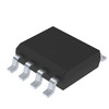
Image may be representation.
See specifications for product details.
EXPRESS OPTION
Payment method

LS2048AXN7V1B - NXP USA Inc.

Manufacturer Part Number
LS2048AXN7V1B
Manufacturer
NXP Semiconductors
Allelco Part Number
98D-LS2048AXN7V1B
Warranty
1 Year Allelco Warranty - Find out more
Stock Status:
38,580 pcs available, New & Original
Parts Description
LS2048A XT 2000 R1.1
Package
1292-FCPBGA (37.5x37.5)
Data sheet
LS2048AXN7V1B.pdf
RoHs Status
ROHS3 Compliant
Our certification
In stock: 38580
  • Unit Price: $431.372
  • Subtotal: $0.00

Want a better price?
Add to Cart and Submit RFQ now, we'll contact you immediately.

Quantity Unit Price Ext. Price
1+ $431.372 $431.37
The above prices does not include taxes and freight rates, which will be calculated on the order pages.


Specifications

LS2048AXN7V1B Tech Specifications
NXP USA Inc. - LS2048AXN7V1B technical specifications, attributes, parameters and parts with similar specifications to NXP USA Inc. - LS2048AXN7V1B

Product Attribute Attribute Value
Manufacturer NXP Semiconductors
Voltage - I/O -
USB USB 3.0 (2) + PHY
Supplier Device Package 1292-FCPBGA (37.5x37.5)
Speed 2.0GHz
Series QorIQ® Layerscape
Security Features -
SATA SATA 6Gbps (2)
RAM Controllers DDR4
Package / Case 1292-BFBGA, FCBGA
Package Tray
Product Attribute Attribute Value
Operating Temperature -40°C ~ 105°C
Number of Cores/Bus Width 4 Core, 64-Bit
Mounting Type Surface Mount
Graphics Acceleration -
Ethernet 10GbE (8) or 1GbE (16) & 2.5GbE (1)
Display & Interface Controllers -
Core Processor ARM® Cortex®-A72
Co-Processors/DSP -
Base Product Number LS2048
Additional Interfaces -

Environmental & Export Classifications

ATTRIBUTE DESCRIPTION
RoHs Status ROHS3 Compliant
Moisture Sensitivity Level (MSL) 3 (168 Hours)
REACH Status REACH Unaffected
HTSUS 0000.00.0000

Frequently Asked Questions(FAQ)

What is the maximum operating temperature for the NXP LS2048AXN7V1B processor, and how does this affect system reliability in industrial environments?
The LS2048AXN7V1B supports an operating temperature range of -40°C to 105°C, which enables reliable performance in demanding industrial and automotive applications. This extended temperature range ensures functionality in harsh conditions where ambient heat or cold could otherwise compromise timing integrity or cause thermal shutdown. At the upper limit of 105°C, designers must ensure adequate thermal management through PCB layout, heatsinking, or airflow to prevent junction temperatures from exceeding safe thresholds, especially under full computational load.
How does the clock speed of the LS2048AXN7V1B compare to other processors in the QorIQ Layerscape series, and what impact does it have on power consumption?
With a maximum clock speed of 2.0GHz across its four ARM Cortex-A72 cores, the LS2048AXN7V1B delivers higher per-core throughput compared to lower-speed variants like the LS2024 or LS2088 models, which typically operate at 1.2GHz or 1.5GHz. However, increased frequency directly correlates with dynamic power consumption—approximately doubling switching activity per cycle—which can raise thermal output by 30–50% under sustained workloads. This trade-off necessitates careful power budgeting in compact systems and may require dynamic voltage and frequency scaling (DVFS) to balance performance and energy efficiency.
What are the key differences between the LS2048AXN7V1B and the LS2024A in terms of core count, memory support, and networking capabilities?
The LS2048AXN7V1B features four ARM Cortex-A72 cores running at 2.0GHz, while the LS2024A has two cores at 1.2GHz, resulting in significantly higher compute density for parallel workloads. Both share DDR4 memory support, but the LS2048AXN7V1B offers eight 10GbE or sixteen 1GbE Ethernet ports alongside one 2.5GbE interface, providing greater flexibility in high-bandwidth network topologies. In contrast, the LS2024A typically includes fewer Ethernet channels and lacks 10GbE capability, making the LS2048AXN7V1B better suited for carrier-grade routers and data center aggregation nodes.
Can the LS2048AXN7V1B be used in aerospace applications, and what certifications or environmental qualifications should be verified?
While the LS2048AXN7V1B is not inherently qualified to MIL-STD standards, its -40°C to 105°C commercial-industrial temperature rating allows use in non-space aerospace subsystems such as avionics enclosures with active thermal control. Designers must still perform derating analysis, implement conformal coating if needed, and validate solder joint reliability under thermal cycling. Compliance with RoHS3 and REACH status confirms material safety but does not equate to functional qualification—additional testing against RTCA DO-160 or ECSS standards would be required for full aerospace certification.
How many SATA ports does the LS2048AXN7V1B support, and what considerations apply when connecting storage devices in a redundant array?
The LS2048AXN7V1B provides two SATA 6Gbps controllers, enabling direct connection of up to two drives without requiring external bridge chips. When building RAID arrays, designers should account for shared bandwidth between SATA and PCIe lanes, as both share root complex resources. Additionally, power sequencing and signal integrity become critical at link rates approaching 6 Gbps—especially over long traces—requiring impedance-controlled routing and proper termination to maintain error-free operation during sustained disk I/O operations.
Is USB 3.0 support included on the LS2048AXN7V1B, and what role does the integrated PHY play in system design?
Yes, the LS2048AXN7V1B integrates two USB 3.0 ports with embedded physical layer (PHY), eliminating the need for discrete transceivers and simplifying board design. The built-in PHY reduces component count, footprint, and cost while maintaining signal integrity over standard FR4 PCBs up to recommended trace lengths. However, designers must still comply with USB 3.0 electrical specifications, including differential pair routing, ground plane stitching, and ESD protection, to avoid compliance failures during host enumeration or data transfer.
What is the package type of the LS2048AXN7V1B, and what challenges arise during PCB assembly?
The LS2048AXN7V1B uses a 1292-ball FCPBGA package measuring 37.5mm × 37.5mm. This fine-pitch BGA requires advanced assembly techniques such as laser-drilled microvias for fan-out routing and strict adherence to IPC Class 3 standards for solder paste printing and reflow profiling. Due to its large size and high pin count, warpage risk increases during thermal cycling, so panelization and stiffeners may be necessary. Moisture sensitivity level (MSL) of 3 mandates baking prior to assembly if stored beyond 168 hours to prevent popcorning defects.
Does the LS2048AXN7V1B include any hardware-based security features, and how can software isolation be achieved without them?
The LS2048AXN7V1B does not integrate dedicated security accelerators like cryptographic engines or trusted execution environments, relying instead on software-based isolation mechanisms. Designers can implement secure boot using signed firmware images validated via SHA-256 hashes, enforce memory partitioning through hypervisors like PetaLinux or Barebox, and utilize ARM TrustZone extensions available on the Cortex-A72 cores. While these provide logical separation, physical tampering risks remain unmitigated without additional hardware modules such as TPMs or HSMs.
How does the choice of DRAM configuration affect boot time and memory bandwidth on the LS2048AXN7V1B?
The LS2048AXN7V1B supports dual-channel DDR4 memory, and selecting appropriately matched DIMMs with consistent rank and bank group configurations minimizes initialization delays during boot. Mismatched timings between channels can trigger fallback modes that reduce effective bandwidth by 30–40%, increasing application startup latency. For optimal performance, symmetric loading across both channels with JEDEC-compliant SPD profiles ensures balanced command scheduling, maximizing theoretical peak bandwidth of approximately 38 GB/s (assuming DDR4-2400 operation).
What is the significance of the "Base Product Number" field being listed as LS2048 for the LS2048AXN7V1B, and how does it relate to part differentiation?
The base product number LS2048 identifies the broader family of devices sharing architectural similarities, including pin-compatible variants with different core counts or clock speeds. The suffix "AXN7V1B" specifies exact feature set, package variant, and process characteristics—such as die revision and manufacturing batch. Understanding this hierarchy helps engineers evaluate upgrade paths, cross-reference errata documents, and assess compatibility across multiple designs using common evaluation platforms like the LS2048A-RDB.
How does the absence of integrated graphics impact the use case of the LS2048AXN7V1B, and what alternatives exist for display output?
Since the LS2048AXN7V1B lacks onboard GPU functionality, any video output must be handled by external controllers connected via PCIe or MIPI interfaces. Common implementations include discrete GPUs for desktop workstations or FPGA-based video encoders for embedded vision systems. This design choice prioritizes raw compute and network throughput over multimedia processing, making the part ideal for server-class or telecom infrastructure rather than consumer multimedia endpoints.
What is the recommended trace length matching requirement for DDR4 signals interfacing with the LS2048AXN7V1B?
DDR4 signal integrity demands tight skew control between data groups and clock lines. For the LS2048AXN7V1B’s dual-channel interface, Fly-by topology with ±50 mil tolerance on clock-to-data skew is typical, though tighter matching (e.g., ±25 mil) improves margin at higher frequencies. Length-matching should also consider return path discontinuities caused by vias or splits in reference planes, which can degrade eye diagrams and increase bit error rates during burst transfers exceeding 10 GB/s.
How does the HTSUS classification (0000.00.0000) listed for the LS2048AXN7V1B affect import/export logistics, and what documentation is typically required?
An HTSUS code of 0000.00.0000 indicates generic classification, implying minimal tariff treatment but requiring detailed commercial invoices specifying technical parameters to justify exemption claims. Importers must still provide certificates of origin, packing lists, and sometimes end-use declarations depending on bilateral trade agreements. While this simplifies initial entry, prolonged customs scrutiny may occur if authorities question the product’s intended function or country of manufacture, particularly under current semiconductor trade restrictions.
What role does dynamic voltage and frequency scaling (DVFS) play when implementing the LS2048AXN7V1B in battery-powered edge devices?
Although the LS2048AXN7V1B targets wired infrastructure rather than mobile platforms, DVFS remains relevant in low-power edge deployments where thermal envelope constrains continuous peak performance. By lowering voltage and reducing frequency during idle periods, average power consumption drops exponentially due to the cubic relationship between voltage and dynamic power. However, aggressive scaling introduces latency penalties during context switches, so firmware must balance responsiveness against energy savings based on workload predictability.
Can the LS2048AXN7V1B directly drive multiple PCIe Gen3 endpoints without a switch, and what limitations apply?
Yes, the LS2048AXN7V1B includes sufficient PCIe Gen3 lanes to connect several downstream devices—up to six x1 links or three x2 links—but direct fan-out without a switch risks bandwidth contention and complex arbitration logic. Without a PCIe switch, all devices share the same root complex bandwidth, potentially creating bottlenecks during concurrent access. A switch chip mitigates this by enabling hierarchical topology and load balancing, essential for scalable systems with multiple SSDs, NICs, or accelerator cards.

Parts with Similar Specifications

The three parts on the right have similar specifications to NXP USA Inc. LS2048AXN7V1B

Product Attribute LS2048AXN711B LS2048ASN7V1B LS2048AXE7V1B LS2048AXE711B
Part Number LS2048AXN711B LS2048ASN7V1B LS2048AXE7V1B LS2048AXE711B
Manufacturer NXP USA Inc. NXP USA Inc. NXP USA Inc. NXP USA Inc.
RAM Controllers - - - -
Additional Interfaces - - - -
Package / Case - 196-LFBGA 16-DIP (0.300', 7.62mm) 64-VFQFN Exposed Pad
Mounting Type - Surface Mount Through Hole Surface Mount
Security Features - - - -
Core Processor - - - -
Package - Tape & Reel (TR) Tube Tape & Reel (TR)
Graphics Acceleration - - - -
Supplier Device Package - 196-NFBGA (12x12) 16-PDIP 64-VQFN (9x9)
Base Product Number - DAC34H84 MAX500 ADS62P42
SATA - - - -
USB - - - -
Speed - - - -
Co-Processors/DSP - - - -
Operating Temperature - -40°C ~ 85°C 0°C ~ 70°C -40°C ~ 85°C
Display & Interface Controllers - - - -
Series - - - -
Voltage - I/O - - - -
Ethernet - - - -
Number of Cores/Bus Width - - - -

LS2048AXN7V1B Datasheet PDF

Download LS2048AXN7V1B pdf datasheets and NXP USA Inc. documentation for LS2048AXN7V1B - NXP USA Inc..

Environmental Information
NXP USA Inc REACH.pdf NXP USA Inc RoHS Cert.pdf

Customer Reviews

Evaluation: 10 Articles

  • ECUb***h
    Sep 22, 2026

    Used for repair of an older automotive ECU. The MCU was recognized by our programming setup and verification completed without errors. The repaired board now starts and communicates normally.

  • RS48***ieldTech
    Sep 16, 2026

    Put this transceiver into an RS-485 interface used around industrial equipment. Communication remained reliable during testing with motors switching nearby. Good result for the replacement board.

  • Logi***b_Chris
    Sep 8, 2026

    Purchased for a Cyclone III development project. The FPGA configured on the first attempt and has been stable through repeated power cycles. No problems with the I/O we are using.

  • Circ***FixerTom
    Sep 2, 2026

    Used this rectifier in a high-current power supply repair. Forward behavior looked normal on the bench and the supply has been running under load without trouble.

  • Retr***UWorks
    Aug 31, 2026

    Needed the exact ST10F269Z2Q6 for servicing an older control unit. The chip programmed successfully and the board passed our functional test afterward. Much easier than redesigning around a newer MCU.

  • Andr***PCBLab
    Aug 28, 2026

    I needed this ADC for an older data acquisition board. Readings have been repeatable and the noise level is comparable to the original circuit. Happy with the purchase.

  • Leat***O'Keefe
    Aug 20, 2026

    one of my hobbies is skydiving. and when i'm skydiving this works great.

  • Ilen***
    Aug 20, 2026

    This product works considerably well. It secretly improves my basketball by a lot.

  • Indu***ialPower
    Aug 17, 2026

    Installed this IGBT module in a power conversion cabinet. Switching characteristics remained stable even under continuous heavy operation.

  • Nikh***ech
    Aug 13, 2026

    Great low-power MCU for portable equipment. Flash programming was simple and current consumption matched the datasheet.

Write a Review

Your Email address will not be published.

Shipment

Delivery Time

In-stock items can be shipped within 24 hours. Some parts will be arranged for delivery within 1-2 days from the date all items arrive at our warehouse. And Allelco ships order once a day at about 17:00, except Sunday. Once the goods are shipped, the estimated delivery time depends on the shipping methods and Delivery destination. The table below shows are the logistic time for some common countries.

Delivery Cost

  1. Use your express account for shipment if you have one.
  2. Use our account for the shipment. Refer to the table below for the approximate charges.
(Different time frame / countries / package size has different price.)

Delivery Method

  1. Global Common Shipment by DHL / UPS / FedEx / TNT / EMS / SF we support.
  2. Others more shipping ways, please get in touch with your customer manager.

Common Countries Logistic Time Reference
Region Country Logistic Time(Day)
America United States 5
Brazil 7
Europe Germany 5
United Kingdom 4
Italy 5
Oceania Australia 6
New Zealand 5
Asia India 4
Japan 4
Middle East Israel 6
DHL & FedEx Shipment Charges Reference
Shipment charges(KG) Reference DHL(USD$)
0.00kg-1.00kg USD$30.00 - USD$60.00
1.00kg-2.00kg USD$40.00 - USD$80.00
2.00kg-3.00kg USD$50.00 - USD$100.00
Note:
The above table is for reference only. There may have some data bias for the uncontrollable factors.
Contact us if you have any questions.
  • QC (Quality Warranty)
  • Payment Support
  • Packaging
  • Certifications & Memberships

QC (Quality Warranty)

Allelco is committed to exceeding customer expectations through customer service excellence, order accuracy, and on-time delivery.
This is achieved through our commitment to the continual improvement of our processes, services, and products.


Strict quality inspection builds a solid foundation for electronic component quality.
  1. Visual inspection
  2. Performance testing and reliability verification
  3. Standardized full-process testing
  4. Precise control of every parameter
We eliminate defective components and ensure the stable operation of electronic devices through professional quality standards.

Payment Support

The payment method can be chosen from the methods shown below: Wire Transfer (T/T, Bank Transfer), Western Union, Credit card, PayPal.
  • HKBea
  • Paypal
  • MasterCard
  • Western-Union
  • VISA
Stable Delivery, Sincere Partnership — Your Faithful Supply Chain Partner
  • Efficient Supply Management
  • Cost-Saving Procurement
  • Fast Sourcing & Delivery
Contact us if you have any questions.

Packaging

Electrostatic Discharge Protection and Handling

All electrostatic-sensitive components are handled in accordance with electrostatic discharge control procedures. The products are hermetically sealed in anti-static safe packaging to prevent electrostatic damage. Appropriate labeling is also applied for identification and traceability. This ensures product integrity during storage, handling and transportation.


ESD

Certifications & Memberships

Third-party certified, strict quality control. Our certification
  • ISO 9001: 2015
  • ISO 13485: 2016
  • ISO 14001: 2015
  • ISO 28000: 2007
  • ISO 45001: 2018
  • GB/T 27922-2011
  • SMTA
  • IPC
  • ESD
  • PSMA
NXP USA Inc.

LS2048AXN7V1B

NXP USA Inc.
98D-LS2048AXN7V1B

Want a better price? Add to Cart and Submit RFQ now, we'll contact you immediately.

0 RFQ
Shopping cart (0 Items)
It is empty.
Compare List (0 Items)
It is empty.
Feedback

Your feedback matters! At Allelco, we value the user experience and strive to improve it constantly.
Please share your comments with us via our feedback form, and we'll respond promptly.
Thank you for choosing Allelco.

Subject
E-mail
Comments
Captcha
Drag or click to upload file
Upload File
types: .xls, .xlsx, .doc, .docx, .jpg, .png and .pdf.
Max file size: 10MB