
Manufacturer Part Number
S9S08DZ60F2CLC
Manufacturer
NXP Semiconductors
Introduction
The S9S08DZ60F2CLC is a high-performance, low-power 8-bit embedded microcontroller from NXP Semiconductors. It features a range of advanced peripherals and connectivity options, making it suitable for a variety of industrial and consumer applications.
Product Features and Performance
8-bit S08 core processor
40MHz operating speed
60KB FLASH program memory
2KB EEPROM
4KB RAM
Integrated CAN, I2C, LIN, SCI, and SPI interfaces
10-channel 12-bit ADC
Low-voltage detection (LVD), power-on reset (POR), PWM, and watchdog timer (WDT) peripherals
25 general-purpose I/O pins
Product Advantages
Flexible connectivity options for a wide range of applications
Robust safety and power management features
High-performance 8-bit core with ample memory
Low power consumption for energy-efficient designs
Key Reasons to Choose This Product
Robust and reliable performance for industrial and consumer applications
Extensive peripheral set for flexible system design
Cost-effective solution for 8-bit embedded systems
Long-term availability and support from NXP Semiconductors
Quality and Safety Features
Industrial-grade operating temperature range (-40°C to 85°C)
Rigorous quality and reliability testing
Integrated safety features like LVD and POR
Compatibility
The S9S08DZ60F2CLC is pin-compatible with other S08 series microcontrollers from NXP, allowing for easy design migration and platform flexibility.
Application Areas
Industrial automation and control
Building and home automation
Appliances and consumer electronics
Automotive and transportation systems
Product Lifecycle
The S9S08DZ60F2CLC is an active product in our website's sales team's portfolio. There are no immediate plans for discontinuation. However, as technology evolves, equivalent or alternative models may become available in the future. Customers are advised to check with our website's sales team for the most up-to-date product information and availability.
 S9S08DZ60F1MLCFreescale SemiconductorIC MCU 8BIT 60KB FLASH 32LQFP
 S9S08DZ60F1MLFNXP USA Inc.IC MCU 8BIT 60KB FLASH 48LQFP
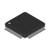 S9S08DZ60F1MLHFreescale SemiconductorIC MCU 8BIT 60KB FLASH 64LQFP
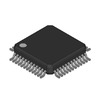 S9S08DZ60F2CLFFreescale SemiconductorIC MCU 8BIT 60KB FLASH 48LQFP
 S9S08DZ60F1VLHNXP USA Inc.IC MCU 8BIT 60KB FLASH 64LQFP
 S9S08DZ60F1MLCNXP USA Inc.IC MCU 8BIT 60KB FLASH 32LQFP
 S9S08DZ60F2MLCNXP USA Inc.IC MCU 8BIT 60KB FLASH 32LQFP
 S9S08DZ60F1MLFFreescale SemiconductorIC MCU 8BIT 60KB FLASH 48LQFP
 S9S08DZ60F1MLHRFreescale / NXP Semiconductors


