View All

Please refer to the English Version as our Official Version.Return

Europe
France(Français) Germany(Deutsch) Italy(Italia) Russian(русский) Poland(polski) Czech(Čeština) Luxembourg(Lëtzebuergesch) Netherlands(Nederland) Iceland(íslenska) Hungarian(Magyarország) Spain(español) Portugal(Português) Turkey(Türk dili) Bulgaria(Български език) Ukraine(Україна) Greece(Ελλάδα) Israel(עִבְרִית) Sweden(Svenska) Finland(Svenska) Finland(Suomi) Romania(românesc) Moldova(românesc) Slovakia(Slovenská) Denmark(Dansk) Slovenia(Slovenija) Slovenia(Hrvatska) Croatia(Hrvatska) Serbia(Hrvatska) Montenegro(Hrvatska) Bosnia and Herzegovina(Hrvatska) Lithuania(lietuvių) Spain(Português) Switzerland(Deutsch) United Kingdom(English)
Asia/Pacific
Japan(日本語) Korea(한국의) Thailand(ภาษาไทย) Malaysia(Melayu) Singapore(Melayu) Vietnam(Tiếng Việt) Philippines(Pilipino)
Africa, India and Middle East
United Arab Emirates(العربية) Iran(فارسی) Tajikistan(فارسی) India(हिंदी) Madagascar(malaɡasʲ)
South America / Oceania
New Zealand(Maori) Brazil(Português) Angola(Português) Mozambique(Português)
North America
United States(English) Canada(English) Haiti(Ayiti) Mexico(español)
HomeProductsIntegrated Circuits (ICs)Embedded - FPGAs (Field Programmable Gate Array)5SGXEA4K2F40C2LG
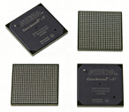
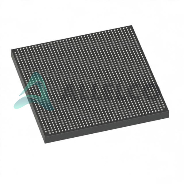
5SGXEA4K2F40C2LG Image
Image may be representation.
See specifications for product details.
EXPRESS OPTION
Payment method

5SGXEA4K2F40C2LG - Intel

Manufacturer Part Number
5SGXEA4K2F40C2LG
Manufacturer
Intel
Allelco Part Number
32D-5SGXEA4K2F40C2LG
Warranty
1 Year Allelco Warranty - Find out more
Stock Status:
5,282 pcs available, New & Original
Parts Description
IC FPGA 696 I/O 1517FBGA
Package
1517-FBGA (40x40)
Data sheet
5SGXEA4K2F40C2L.pdf
RoHs Status
RoHS Compliant
Our certification
In stock: 5282

Required fields are indicated by an asterisk (*)
Please send RFQ, we will respond immediately.

Quantity

Specifications

5SGXEA4K2F40C2LG Tech Specifications
Intel - 5SGXEA4K2F40C2LG technical specifications, attributes, parameters and parts with similar specifications to Intel - 5SGXEA4K2F40C2LG

Product Attribute Attribute Value
Manufacturer Intel
Voltage - Supply 0.82V ~ 0.88V
Total RAM Bits 37888000
Supplier Device Package 1517-FBGA (40x40)
Series Stratix® V GX
Package / Case 1517-BBGA, FCBGA
Package Tray
Product Attribute Attribute Value
Operating Temperature 0°C ~ 85°C (TJ)
Number of Logic Elements/Cells 420000
Number of LABs/CLBs 158500
Number of I/O 696
Mounting Type Surface Mount
Base Product Number 5SGXEA4

Environmental & Export Classifications

ATTRIBUTE DESCRIPTION
RoHs Status RoHS Compliant
Moisture Sensitivity Level (MSL) 3 (168 Hours)
REACH Status REACH Unaffected

Parts Introduction

5SGXEA4K2F40C2LG Image
5SGXEA4K2F40C2LG (1)

Manufacturer Part Number

5SGXEA4K2F40C2LG

Manufacturer

intel

Introduction

The intel 5SGXEA4K2F40C2LG is a high-performance embedded FPGA (Field Programmable Gate Array) that offers advanced features and capabilities for a wide range of applications. This Stratix® V GX series FPGA provides exceptional logic density, advanced memory, and advanced I/O capabilities, making it a versatile solution for demanding embedded systems.

Product Features and Performance

158,500 Logic Array Blocks (LABs) / Configurable Logic Blocks (CLBs)

420,000 Logic Elements/Cells

37,888,000 Total RAM Bits

696 I/O Pins

Operating Voltage: 0.82V ~ 0.88V

Operating Temperature: 0°C ~ 85°C (TJ)

1517-BBGA, FCBGA Package, 1517-FBGA (40x40) Supplier Device Package

Product Advantages

High logic density and performance for complex embedded applications

Extensive on-chip memory and advanced I/O capabilities

Flexibility and programmability for customized hardware solutions

Low power consumption for energy-efficient designs

Key Reasons to Choose This Product

Industry-leading Stratix® V FPGA technology from intel

Robust feature set and performance for demanding embedded systems

Proven reliability and longevity in the market

Comprehensive development tools and support from intel

Quality and Safety Features

Rigorous quality control and testing processes

Compliance with industry safety standards and regulations

Compatibility

This FPGA is compatible with a wide range of embedded systems and applications, including industrial automation, communication systems, and medical devices.

Application Areas

Industrial automation and control

Communication and networking equipment

Medical and scientific instrumentation

Aerospace and defense systems

Automotive and transportation applications

Product Lifecycle

The 5SGXEA4K2F40C2LG is an active product in intel's Stratix® V GX series. There are no known plans for discontinuation at this time. If you require information about equivalent or alternative models, please contact our sales team through our website for the latest updates.

Frequently Asked Questions(FAQ)

How does the 5SGXEA4K2F40C2LG compare to other Stratix V GX FPGAs in terms of logic density and I/O availability for high-performance computing applications?
The 5SGXEA4K2F40C2LG features 420,000 logic elements and 158,500 LABs, providing substantial logic density suitable for complex algorithmic implementations. With 696 user-accessible I/Os, it supports high-bandwidth communication interfaces such as PCIe Gen3 and 10 Gigabit Ethernet. Compared to lower-density variants like the 5SGXEB4, this model offers approximately 30% more logic resources, making it preferable when designs require extensive signal processing or large state machines without resorting to multi-device stacking.
What are the key thermal and power considerations when deploying the 5SGXEA4K2F40C2LG in industrial control systems operating at elevated ambient temperatures?
Operating within a junction temperature range of 0°C to 85°C, the 5SGXEA4K2F40C2LG must be evaluated under worst-case power dissipation scenarios. At full utilization, typical dynamic power consumption can reach 25–30 W depending on switching activity and I/O loading. Thermal management requires careful PCB layout with proper heat-spreading layers and potentially forced airflow. The tightly packed 1517-FBGA package complicates solder joint reliability under thermal cycling, necessitating adherence to JEDEC MSL 3 handling protocols during assembly.
Can the 5SGXEA4K2F40C2LG support hard intellectual property (IP) blocks such as transceivers and memory controllers without significant resource overhead?
Yes, the Stratix V architecture integrates hardened transceivers supporting data rates up to 28.3 Gbps across its transceiver tiles, which consume negligible logic elements compared to soft implementations. Hard DDR3/DDR4 memory controllers and PCIe endpoints are available via Quartus Prime IP libraries, reducing both latency and FPGA logic utilization. However, enabling these hard blocks may reduce available general-purpose routing flexibility if not carefully planned.
In what scenarios would selecting the 5SGXEA4K2F40C2LG over an ASIC be justified despite higher unit costs?
The 5SGXEA4K2F40C2LG is advantageous when time-to-market pressure outweighs long-term NRE savings, especially for prototyping or low-to-medium volume production runs. Its reprogrammability allows rapid design iteration, and the presence of hardened transceivers reduces development risk for protocol-intensive applications like telecom line cards or medical imaging systems. For volumes below 10,000 units, FPGA cost per function often competes favorably due to reduced board complexity and faster validation cycles.
How should clock domain crossing (CDC) be managed in designs using the 5SGXEA4K2F40C2LG given its global and regional clock networks?
The 5SGXEA4K2F40C2LG provides multiple dedicated global and regional clock networks that minimize skew and jitter but require disciplined CDC practices. Synchronization primitives such as Intel’s Clock Crossing Assistant should be used for asynchronous signals between domains. Dual-clock FIFOs implemented with built-in handshake logic are recommended for data transfers, as they leverage internal block memory efficiently while avoiding metastability risks inherent in direct register sampling.
What impact does partial reconfiguration have on system-level reliability when using the 5SGXEA4K2F40C2LG in safety-critical applications?
Partial reconfiguration (PR) enables runtime functionality updates without halting the entire device, useful for adaptive systems. However, PR introduces timing closure challenges and increases susceptibility to configuration bitstream corruption if not protected. The 5SGXEA4K2F40C2LG supports PR regions defined in QSF files, but frequent reconfigurations may degrade flash endurance in external configuration devices. Redundant checksum verification and rollback mechanisms are essential for mission-critical deployments.
Is it possible to implement high-speed serial links exceeding 25 Gbps using the 5SGXEA4K2F40C2LG, and what design constraints apply?
While the 5SGXEA4K2F40C2LG supports transceivers up to 28.3 Gbps, achieving reliable operation above 25 Gbps demands strict channel integrity measures. Signal loss, crosstalk, and impedance mismatches become dominant factors at these rates. Differential pairs must maintain controlled impedance (typically 100 Ω), and trace lengths should be matched within ±50 mils. Equalization settings (CTLE and DFE) must be calibrated per link partner, and reference clock stability is critical—usually requiring a ±50 ppm crystal oscillator.
How does the 5SGXEA4K2F40C2LG perform in terms of power efficiency compared to newer-generation FPGAs from alternative vendors?
The 5SGXEA4K2F40C2LG achieves competitive power efficiency for its class, delivering approximately 0.6 µW per logic element under moderate activity. Its use of TSMC's 28 HPM process node enables lower static leakage than earlier nodes, but dynamic power remains proportional to frequency and capacitive load. When compared to Xilinx UltraScale+ or Lattice CertusPRO, this device trades off newer architectural features (e.g., hardened AI engines) for proven transceiver performance in legacy-compatible ecosystems.
What precautions are necessary during FPGA configuration boot-up sequences involving the 5SGXEA4K2F40C2LG?
The 5SGXEA4K2F40C2LG initiates configuration through a master serial mode typically using an EPCS128 or similar flash device. During power-up, the CCLK pin must stabilize before the configuration clock begins, and POR (Power-On Reset) delays must be respected to ensure stable supply rails. Failure to meet timing can result in incomplete configuration or device hang. Additionally, the nSTATUS and CONF_DONE pins should be monitored to confirm successful initialization before releasing user logic.
Can the 5SGXEA4K2F40C2LG interface directly with DDR4 memory modules, and what performance trade-offs exist?
Yes, the 5SGXEA4K2F40C2LG includes hardened DDR4 memory controllers capable of supporting up to 1600 MT/s data rates. These controllers offload PHY-layer responsibilities such as calibration and DLL synchronization, reducing FPGA resource usage by up to 40% compared to soft implementations. However, board-level compliance with JEDEC DDR4 electrical standards is mandatory, and termination schemes must be carefully implemented to avoid signal integrity degradation at higher speeds.
What level of ESD protection is recommended when handling the 5SGXEA4K2F40C2LG in production environments?
As an MSL 3 component with a 168-hour floor life, the 5SGXEA4K2F40C2LG requires anti-static precautions beyond standard packaging. Handling should occur only after full discharge, and workstations must maintain grounded wrist straps and conductive flooring. Storage in dry cabinets with humidity control (30–60% RH) preserves solder joint integrity. Although the FBGA package has some inherent robustness, direct human contact during unpacking poses risk of latent damage not immediately apparent.
How do routing congestion patterns differ between the 5SGXEA4K2F40C2LG and smaller Stratix V variants when implementing wide bus architectures?
The 5SGXEA4K2F40C2LG’s dense interconnect fabric handles wide buses more efficiently than smaller variants due to increased backbone switch capacity. However, long combinatorial paths spanning multiple LAB clusters can still suffer from increased delay unless pipelined. The larger die size also means longer average net lengths, which may affect timing closure margins. Placement constraints should prioritize grouping related functional blocks near shared clock regions to minimize routing hops.
What role does the internal block RAM play in optimizing performance-critical algorithms on the 5SGXEA4K2F40C2LG?
The 5SGXEA4K2F40C2LG contains 37.9 million bits of embedded block RAM organized into 1,894 blocks of 20 kbits each. This memory serves dual purposes: storing lookup tables, FIFO buffers, and intermediate data structures. By keeping frequently accessed data close to processing logic, block RAM reduces reliance on external SRAM and minimizes access latency. Careful partitioning ensures balanced utilization across the device, preventing localized saturation that could force inefficient distributed RAM usage.
Are there any known limitations in using JTAG debugging tools with the 5SGXEA4K2F40C2LG during active high-speed transmission?
Active JTAG debugging can interfere with high-speed serial links on the 5SGXEA4K2F40C2LG because JTAG signals share the same physical pins as transceiver channels in some configurations. Disabling JTAG during transceiver operation or using boundary scan isolation is advisable. Alternatively, dedicated debug cores like SignalTap II can capture internal signals without affecting external interfaces, provided sufficient trigger conditions are defined and memory depth accommodates expected event durations.
What steps are required to ensure compliance with RoHS and REACH regulations when sourcing the 5SGXEA4K2F40C2LG for European market deployment?
The 5SGXEA4K2F40C2LG is certified RoHS compliant, meaning it contains no restricted substances above threshold limits. REACH status indicates no SVHCs (Substances of Very High Concern) declared above 0.1% weight-by-weight. Suppliers must provide full material declarations upon request, and procurement records should include certificates of conformance. End-of-life documentation should confirm recyclability pathways aligned with WEEE directives.
How does the 5SGXEA4K2F40C2LG handle transient voltage spikes on its 0.82V–0.88V core supply rail?
The core voltage tolerance window is narrow (±3%), so transient events must be suppressed below 0.95 V absolute maximum ratings. On-die decoupling capacitors mitigate short-term dips, but sustained deviations cause functional failure or permanent damage. Power sequencing must follow Intel-recommended guidelines—core voltage stabilizes before I/O voltages—to prevent latch-up conditions. External TVS diodes or ferrite beads combined with bulk capacitance are advised for harsh environments.
What design tools and constraints files are essential when integrating the 5SGXEA4K2F40C2LG into a new project?
Quartus Prime Pro Edition is required for full feature support, including place-and-route optimization for high-speed I/O. Device-specific SDC constraint templates define valid operating ranges for clocks, voltages, and I/O standards. Pin assignments must align with the 1517-FBGA footprint, and thermal models help estimate junction temperatures under various workloads. Additionally, IBIS models for I/O buffers aid in pre-layout signal integrity analysis prior to board fabrication.
Can the 5SGXEA4K2F40C2LG be safely used in aerospace or defense applications requiring radiation hardening?
No, the 5SGXEA4K2F40C2LG is not qualified for radiation environments. Single-event upsets (SEUs) can alter configuration memory contents without mitigation. For space or military use, Intel offers radiation-tolerant alternatives such as the RTG4 family or third-party solutions like Microsemi RTAX-S. If unavoidable, triple modular redundancy (TMR) and scrubbing circuits can reduce SEU probability but add significant area and latency overhead.

Parts with Similar Specifications

The three parts on the right have similar specifications to Intel 5SGXEA4K2F40C2LG

Product Attribute 5SGXEA4K2F40C2L 5SGXEA4K2F40C2G 5SGXEA4K2F40I2LG 5SGXEA4K2F40C2LN
Part Number 5SGXEA4K2F40C2L 5SGXEA4K2F40C2G 5SGXEA4K2F40I2LG 5SGXEA4K2F40C2LN
Manufacturer Intel Intel Intel Intel
Series - - - -
Base Product Number - DAC34H84 MAX500 ADS62P42
Mounting Type - Surface Mount Through Hole Surface Mount
Number of LABs/CLBs - - - -
Package - Tape & Reel (TR) Tube Tape & Reel (TR)
Total RAM Bits - - - -
Operating Temperature - -40°C ~ 85°C 0°C ~ 70°C -40°C ~ 85°C
Number of I/O - - - -
Package / Case - 196-LFBGA 16-DIP (0.300', 7.62mm) 64-VFQFN Exposed Pad
Number of Logic Elements/Cells - - - -
Voltage - Supply - - - -
Supplier Device Package - 196-NFBGA (12x12) 16-PDIP 64-VQFN (9x9)

5SGXEA4K2F40C2LG Datasheet PDF

Download 5SGXEA4K2F40C2LG pdf datasheets and Intel documentation for 5SGXEA4K2F40C2LG - Intel.

PCN Design/Specification
Mult Dev Software Chgs 3/Jun/2021.pdf Quartus SW/Web Chgs 23/Sep/2021.pdf

Customer Reviews

Evaluation: 10 Articles

  • ECUb***h
    Sep 22, 2026

    Used for repair of an older automotive ECU. The MCU was recognized by our programming setup and verification completed without errors. The repaired board now starts and communicates normally.

  • RS48***ieldTech
    Sep 16, 2026

    Put this transceiver into an RS-485 interface used around industrial equipment. Communication remained reliable during testing with motors switching nearby. Good result for the replacement board.

  • Logi***b_Chris
    Sep 8, 2026

    Purchased for a Cyclone III development project. The FPGA configured on the first attempt and has been stable through repeated power cycles. No problems with the I/O we are using.

  • Circ***FixerTom
    Sep 2, 2026

    Used this rectifier in a high-current power supply repair. Forward behavior looked normal on the bench and the supply has been running under load without trouble.

  • Retr***UWorks
    Aug 31, 2026

    Needed the exact ST10F269Z2Q6 for servicing an older control unit. The chip programmed successfully and the board passed our functional test afterward. Much easier than redesigning around a newer MCU.

  • Andr***PCBLab
    Aug 28, 2026

    I needed this ADC for an older data acquisition board. Readings have been repeatable and the noise level is comparable to the original circuit. Happy with the purchase.

  • Leat***O'Keefe
    Aug 20, 2026

    one of my hobbies is skydiving. and when i'm skydiving this works great.

  • Ilen***
    Aug 20, 2026

    This product works considerably well. It secretly improves my basketball by a lot.

  • Indu***ialPower
    Aug 17, 2026

    Installed this IGBT module in a power conversion cabinet. Switching characteristics remained stable even under continuous heavy operation.

  • Nikh***ech
    Aug 13, 2026

    Great low-power MCU for portable equipment. Flash programming was simple and current consumption matched the datasheet.

Write a Review

Your Email address will not be published.

Shipment

Delivery Time

In-stock items can be shipped within 24 hours. Some parts will be arranged for delivery within 1-2 days from the date all items arrive at our warehouse. And Allelco ships order once a day at about 17:00, except Sunday. Once the goods are shipped, the estimated delivery time depends on the shipping methods and Delivery destination. The table below shows are the logistic time for some common countries.

Delivery Cost

  1. Use your express account for shipment if you have one.
  2. Use our account for the shipment. Refer to the table below for the approximate charges.
(Different time frame / countries / package size has different price.)

Delivery Method

  1. Global Common Shipment by DHL / UPS / FedEx / TNT / EMS / SF we support.
  2. Others more shipping ways, please get in touch with your customer manager.

Common Countries Logistic Time Reference
Region Country Logistic Time(Day)
America United States 5
Brazil 7
Europe Germany 5
United Kingdom 4
Italy 5
Oceania Australia 6
New Zealand 5
Asia India 4
Japan 4
Middle East Israel 6
DHL & FedEx Shipment Charges Reference
Shipment charges(KG) Reference DHL(USD$)
0.00kg-1.00kg USD$30.00 - USD$60.00
1.00kg-2.00kg USD$40.00 - USD$80.00
2.00kg-3.00kg USD$50.00 - USD$100.00
Note:
The above table is for reference only. There may have some data bias for the uncontrollable factors.
Contact us if you have any questions.
  • QC (Quality Warranty)
  • Payment Support
  • Packaging
  • Certifications & Memberships

QC (Quality Warranty)

Allelco is committed to exceeding customer expectations through customer service excellence, order accuracy, and on-time delivery.
This is achieved through our commitment to the continual improvement of our processes, services, and products.


Strict quality inspection builds a solid foundation for electronic component quality.
  1. Visual inspection
  2. Performance testing and reliability verification
  3. Standardized full-process testing
  4. Precise control of every parameter
We eliminate defective components and ensure the stable operation of electronic devices through professional quality standards.

Payment Support

The payment method can be chosen from the methods shown below: Wire Transfer (T/T, Bank Transfer), Western Union, Credit card, PayPal.
  • HKBea
  • Paypal
  • MasterCard
  • Western-Union
  • VISA
Stable Delivery, Sincere Partnership — Your Faithful Supply Chain Partner
  • Efficient Supply Management
  • Cost-Saving Procurement
  • Fast Sourcing & Delivery
Contact us if you have any questions.

Packaging

Electrostatic Discharge Protection and Handling

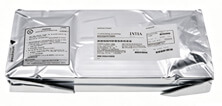
All electrostatic-sensitive components are handled in accordance with electrostatic discharge control procedures. The products are hermetically sealed in anti-static safe packaging to prevent electrostatic damage. Appropriate labeling is also applied for identification and traceability. This ensures product integrity during storage, handling and transportation.


ESD

Certifications & Memberships

Third-party certified, strict quality control. Our certification
  • ISO 9001: 2015
  • ISO 13485: 2016
  • ISO 14001: 2015
  • ISO 28000: 2007
  • ISO 45001: 2018
  • GB/T 27922-2011
  • SMTA
  • IPC
  • ESD
  • PSMA
5SGXEA4K2F40C2LG Image

5SGXEA4K2F40C2LG

Intel
32D-5SGXEA4K2F40C2LG

Want a better price? Add to Cart and Submit RFQ now, we'll contact you immediately.

0 RFQ
Shopping cart (0 Items)
It is empty.
Compare List (0 Items)
It is empty.
Feedback

Your feedback matters! At Allelco, we value the user experience and strive to improve it constantly.
Please share your comments with us via our feedback form, and we'll respond promptly.
Thank you for choosing Allelco.

Subject
E-mail
Comments
Captcha
Drag or click to upload file
Upload File
types: .xls, .xlsx, .doc, .docx, .jpg, .png and .pdf.
Max file size: 10MB