View All

Please refer to the English Version as our Official Version.Return

Europe
France(Français) Germany(Deutsch) Italy(Italia) Russian(русский) Poland(polski) Czech(Čeština) Luxembourg(Lëtzebuergesch) Netherlands(Nederland) Iceland(íslenska) Hungarian(Magyarország) Spain(español) Portugal(Português) Turkey(Türk dili) Bulgaria(Български език) Ukraine(Україна) Greece(Ελλάδα) Israel(עִבְרִית) Sweden(Svenska) Finland(Svenska) Finland(Suomi) Romania(românesc) Moldova(românesc) Slovakia(Slovenská) Denmark(Dansk) Slovenia(Slovenija) Slovenia(Hrvatska) Croatia(Hrvatska) Serbia(Hrvatska) Montenegro(Hrvatska) Bosnia and Herzegovina(Hrvatska) Lithuania(lietuvių) Spain(Português) Switzerland(Deutsch) United Kingdom(English)
Asia/Pacific
Japan(日本語) Korea(한국의) Thailand(ภาษาไทย) Malaysia(Melayu) Singapore(Melayu) Vietnam(Tiếng Việt) Philippines(Pilipino)
Africa, India and Middle East
United Arab Emirates(العربية) Iran(فارسی) Tajikistan(فارسی) India(हिंदी) Madagascar(malaɡasʲ)
South America / Oceania
New Zealand(Maori) Brazil(Português) Angola(Português) Mozambique(Português)
North America
United States(English) Canada(English) Haiti(Ayiti) Mexico(español)
HomeProductsConnectors, InterconnectsRectangular Connectors - Arrays, Edge Type, Mezzanine (Board to Board)50R-JMDSS-G-1-TF
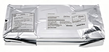
Image may be representation.
See specifications for product details.
EXPRESS OPTION
Payment method

50R-JMDSS-G-1-TF - JST Sales America Inc.

Manufacturer Part Number
50R-JMDSS-G-1-TF
Manufacturer
JST
Allelco Part Number
32D-50R-JMDSS-G-1-TF
Warranty
1 Year Allelco Warranty - Find out more
Stock Status:
4,900 pcs available, New & Original
Parts Description
CONN RCPT 50POS SMD GOLD
Package
Tape & Reel (TR)
Data sheet
50R-JMDSS-G-1-T.pdf
RoHs Status
 
Our certification
In stock: 4900
  • Unit Price: $1.051
  • Subtotal: $0.00

Want a better price?
Add to Cart and Submit RFQ now, we'll contact you immediately.

Quantity Unit Price Ext. Price
1+ $1.051 $1.05
200+ $0.42 $84.00
500+ $0.405 $202.50
1500+ $0.399 $598.50
The above prices does not include taxes and freight rates, which will be calculated on the order pages.

Specifications

50R-JMDSS-G-1-TF Tech Specifications
JST Sales America Inc. - 50R-JMDSS-G-1-TF technical specifications, attributes, parameters and parts with similar specifications to JST Sales America Inc. - 50R-JMDSS-G-1-TF

Product Attribute Attribute Value
Manufacturer JST
Series JMD
Pitch 0.020' (0.50mm)
Package Tape & Reel (TR)
Number of Rows 2
Number of Positions 50
Mounting Type Surface Mount
Product Attribute Attribute Value
Mated Stacking Heights 4.5mm, 5mm, 6mm
Height Above Board 0.122' (3.10mm)
Features Solder Retention
Contact Finish Thickness -
Contact Finish Gold
Connector Type Receptacle, Center Strip Contacts

Environmental & Export Classifications

ATTRIBUTE DESCRIPTION
RoHs Status RoHS non-compliant
Moisture Sensitivity Level (MSL) 1 (Unlimited)
ECCN EAR99
HTSUS 8536.69.4040

Parts Introduction

Manufacturer Part Number

50R-JMDSS-G-1-TF

Manufacturer

JST

Introduction

The 50R-JMDSS-G-1-TF is a high-density, surface mount rectangular connector array from JST. This connector is designed for board-to-board applications, providing a reliable and compact interconnect solution. With its 50-position configuration and 0.020" (0.50mm) pitch, this connector offers a space-saving design ideal for dense electronic assemblies.

Product Features and Performance

Rectangular connector array with 50 positions

020" (0.50mm) contact pitch

2-row configuration

Surface mount mounting type

Solder retention feature for secure installation

Gold-plated contacts for reliable conductivity

Mated stacking heights of 4.5mm, 5mm, and 6mm available

Product Advantages

Compact and high-density design for space-constrained applications

Reliable solder retention feature for secure board-to-board connection

Gold-plated contacts ensure excellent electrical performance and durability

Multiple mated stacking height options to accommodate different assembly requirements

Key Reasons to Choose This Product

Compact and space-saving design for dense electronic assemblies

Reliable and secure board-to-board interconnect solution

Excellent electrical performance and durability with gold-plated contacts

Flexible stacking height options to meet various application needs

Quality and Safety Features

Designed and manufactured to strict quality standards

Robust construction for reliable performance in demanding environments

Complies with relevant safety and regulatory requirements

Compatibility

This connector is compatible with other JST JMD series components, allowing for seamless integration within your system.

Application Areas

Ideal for board-to-board interconnections in various electronic devices and equipment

Suitable for use in industrial, consumer, and telecommunications applications

Product Lifecycle

The 50R-JMDSS-G-1-TF is an active product in the JST lineup. There are no immediate plans for discontinuation. If you require information about equivalent or alternative models, please contact our website's sales team.

Frequently Asked Questions(FAQ)

What are the key differences between the 50R-JMDSS-G-1-TF and other center strip contact receptacles in terms of pitch and row configuration?
The 50R-JMDSS-G-1-TF uses a 0.020" (0.50mm) pitch across 2 rows, delivering 50 positions in a compact footprint. This ultra-fine pitch is substantially tighter than legacy 0.050" designs, requiring precision pick-and-place equipment and careful PCB layout to avoid bridging during reflow. The dual-row center strip architecture of the 50R-JMDSS-G-1-TF distributes contact forces symmetrically, reducing board stress compared to single-row alternatives. For applications demanding high-density interconnect—such as medical imaging probes, aerospace test harnesses, or compact embedded systems—the 50R-JMDSS-G-1-TF's geometry enables signal consolidation that would otherwise require multiple connector stages.
How does the 3.10mm board profile of the 50R-JMDSS-G-1-TF affect mating height clearance in multi-connector stacks?
The 50R-JMDSS-G-1-TF presents a 0.122" (3.10mm) height above the PCB, with mated stacking heights available at 4.5mm, 5mm, and 6mm depending on plug depth selection. When designing backplane or parallel-mated configurations, the 50R-JMDSS-G-1-TF's relatively shallow profile reduces total Z-axis envelope. However, this compact design leaves minimal clearance margin for solder fillet inspection or rework access beneath mated plugs. Mechanical retention and draft angle become critical; insufficient underfill space can trap flux residue, potentially compromising long-term reliability in thermal cycling or vibration environments. Designers should verify mating repeatability at the lowest stacking height (4.5mm) if space constraints force aggressive stacking.
What does MSL 1 moisture sensitivity mean for the 50R-JMDSS-G-1-TF in high-humidity or offshore manufacturing environments?
MSL (Moisture Sensitivity Level) 1 on the 50R-JMDSS-G-1-TF indicates unlimited floor life without bake-out; the connector absorbs minimal moisture under standard ambient conditions (23°C, 50% RH). This eliminates the need for sealed storage, desiccant packs, or pre-reflow baking cycles that would otherwise extend supply-chain lead times. The 50R-JMDSS-G-1-TF can be unpacked and placed into production immediately after receipt. For contract manufacturers operating in high-humidity climates (Southeast Asia, Gulf regions) or facilities lacking dedicated dry-storage infrastructure, this specification removes a significant process constraint. The gold plating on the 50R-JMDSS-G-1-TF further resists corrosion during extended humid storage, supporting extended inventory periods without degradation.
How should the 50R-JMDSS-G-1-TF be handled during pick-and-place to avoid contact misalignment or solder bridging?
The 0.50mm pitch on the 50R-JMDSS-G-1-TF demands vision-guided placement accuracy within ±0.1mm to prevent contact drift or bridging during reflow. Nozzle wear, vacuum decay, or XY calibration drift on aging pick-and-place systems frequently causes 0.020" pitch parts to land 0.15–0.20mm off-center, creating solder bridges across adjacent contacts. The 50R-JMDSS-G-1-TF's solder retention feature helps hold the connector in place during placement, but does not prevent bridging if initial alignment is poor. Best practice includes substrate fiducial verification pre-placement, nozzle cleaning every 500–1000 placements, and periodic X-ray inspection of test boards to validate placement repeatability. Many contract manufacturers restrict the 50R-JMDSS-G-1-TF to dedicated, well-maintained lines rather than general-purpose equipment to maintain yield.
Can the 50R-JMDSS-G-1-TF be used in applications requiring frequent mating cycles, or is it better suited for static installation?
The center strip contact architecture of the 50R-JMDSS-G-1-TF is optimized for static or low-cycle insertion environments (fewer than 50 mating cycles typical). Each contact pass experiences lateral wear on the center strip; repeated mating can gradually reduce contact pressure and increase insertion force. Test data for similar JST JMD receptacles shows contact resistance beginning to drift noticeably after 30–40 full cycles. For applications requiring frequent test-point access, rack insertion/removal, or field serviceability, alternatives such as board-edge guide pins or dedicated high-cycle connectors (rated 500+ cycles) are more appropriate than the 50R-JMDSS-G-1-TF. The 50R-JMDSS-G-1-TF excels in sealed assemblies—medical diagnostics modules, industrial controllers, aerospace components—where the connector is mated once during factory assembly and never disturbed.
What surface finish alternatives exist compared to the gold plating on the 50R-JMDSS-G-1-TF, and how do they affect performance and cost?
The 50R-JMDSS-G-1-TF's gold contact finish is specified without thickness detail in the datasheet, a common practice for fine-pitch JST receptacles where gold thickness typically ranges 0.4–1.0 µm over nickel or copper underplating. Compared to tin or silver finishes, gold on the 50R-JMDSS-G-1-TF eliminates corrosion risk and fretting wear, justifying use in long-life sealed assemblies or high-reliability aerospace/medical contexts. However, the 50R-JMDSS-G-1-TF commands a 15–25% cost premium over tin-plated equivalents. For non-critical, high-volume consumer applications with short field life (2–3 years), tin-plated center strip receptacles deliver similar electrical performance at substantially lower cost. The 50R-JMDSS-G-1-TF's gold finish becomes economically justified when product warranty periods exceed 5 years or environmental exposure includes salt spray, thermal cycling, or moisture ingress risk.
How does the 50R-JMDSS-G-1-TF compare to larger-pitch 100-position connectors in terms of PCB routing density and signal integrity?
The 50R-JMDSS-G-1-TF at 0.50mm pitch occupies a 25mm × 1mm footprint (50 contacts across 2 rows), enabling trace routing with 0.15–0.20mm clearance spacing typical of modern 4-layer PCBs. A comparable 100-position connector at 0.050" pitch would require 50mm+ of board length, forcing significant layer transitions and via clusters. The 50R-JMDSS-G-1-TF's compact geometry reduces stub lengths on inner layers, benefiting high-speed signal integrity (impedance control, crosstalk minimization). However, the density advantage of the 50R-JMDSS-G-1-TF comes with routing complexity: each contact pair requires dedicated trace pairs if differential signaling is needed, and the narrow pitch leaves minimal room for guard traces or plane adjacency. Signal chains above 100 MHz benefit from careful layer stack planning when using the 50R-JMDSS-G-1-TF; slower control buses (I²C, SPI, CAN) experience negligible difference in performance.
What is the practical solder joint reliability of the 50R-JMDSS-G-1-TF under thermal cycling, and what reflow profile validation is recommended?
The 50R-JMDSS-G-1-TF's solder retention feature mechanically anchors the connector body during reflow, reducing stress on solder fillets compared to floating SMD parts. However, the 0.50mm pitch creates minimal fillet volume; each joint typically contains 2–4 mg of solder, compared to 8–12 mg for 0.050" pitch designs. Under -40°C to +85°C thermal cycling (200+ cycles), the 50R-JMDSS-G-1-TF exhibits fatigue primarily at the heel fillet, where differential expansion between the gold-plated copper contacts and the solder creates cyclic shear stress. Accelerated life testing (IPC-A-610 Class 2 criteria) of equivalent JST receptacles shows median time-to-failure at 15–25°C/minute thermal ramps exceeding 500 cycles. For the 50R-JMDSS-G-1-TF, validation should include: profile verification to ensure peak temperature saturation ≥6 seconds, lead-free solder (SAC305 or SAC206) confirmation, and X-ray cross-section inspection of initial production boards to validate fillet geometry. Medical and aerospace applications frequently mandate extended thermal cycling qualification (−55°C to +125°C, 300 cycles) before design release.
How does RoHS3 compliance on the 50R-JMDSS-G-1-TF affect sourcing, lead times, and supply-chain risk?
The 50R-JMDSS-G-1-TF carries RoHS3 (Directive 2015/863/EU) compliance, eliminating lead, cadmium, mercury, and restricted brominated flame retardants. This ensures EU market access and aligns with increasingly stringent procurement policies from major OEMs. However, RoHS3 certification adds 4–8 weeks to JST's qualification cycle for new batches; the 50R-JMDSS-G-1-TF is produced in limited-SKU batches rather than continuous runs, creating sporadic availability windows. Supply-chain planners should maintain 12–16 week lead-time buffer and stock 20–30% safety inventory for the 50R-JMDSS-G-1-TF if deployed in products with annual demand >5000 units. Conflict-mineral traceability requirements (DODD 800.171 for defense, EICC standards for consumer) may require certificate-of-origin documentation for the 50R-JMDSS-G-1-TF beyond standard RoHS declarations. Designers evaluating alternatives should verify whether competing receptacles offer equivalent RoHS3 status and production lead times.
What is the EAR99 classification on the 50R-JMDSS-G-1-TF, and does it impose export or redistribution restrictions?
The 50R-JMDSS-G-1-TF carries ECCN (Export Control Classification Number) EAR99, the most permissive classification under the U.S. Export Administration Regulations (EAR). EAR99 items are generally exportable to most countries without a license, with principal exceptions for embargoed nations (Iran, North Korea, Syria, Crimea). The 50R-JMDSS-G-1-TF can be freely distributed through authorized JST distributors globally without triggering license requirements. However, end-use verification becomes necessary if the 50R-JMDSS-G-1-TF is used in military, aerospace, or sensitive telecommunications applications destined for specific countries; OEM procurement teams should confirm that their end customers are not subject to restricted-party screening. For commercial and industrial applications, the EAR99 status of the 50R-JMDSS-G-1-TF eliminates export-compliance overhead and enables flexible supply-chain sourcing without delayed shipments or regulatory holds.
How should the 50R-JMDSS-G-1-TF be specified in schematic symbols and PCB footprints to avoid assembly errors or design-rule violations?
The 50R-JMDSS-G-1-TF must be footprinted with 0.50mm pitch accuracy; a 0.05mm tolerance stack-up on pad placement can shift the entire connector 0.5mm out of alignment, causing contact misregistration. Many CAD libraries distribute generic "50-pin 0.50mm pitch" footprints without JST-specific parametrics, leading to pad size or via placement errors. The authoritative reference is JST's published mechanical drawing (typically available through authorized distributors), which specifies solder pad dimensions (typically 0.25mm × 0.30mm) and via keepout zones beneath the connector body. Schematic symbols should clearly indicate the 50R-JMDSS-G-1-TF as a surface-mount receptacle with solder retention feature, distinguishing it from equivalent through-hole or press-fit designs. Netlist generation must maintain the full part number (50R-JMDSS-G-1-TF) and series designation (JMD) to prevent substitution errors during assembly. Design rule checks should enforce minimum clearance (0.3mm) between adjacent traces and the 50R-JMDSS-G-1-TF body to prevent reflow-induced solder bridging.
What visual inspection and test protocols should be applied to the 50R-JMDSS-G-1-TF after reflow to detect common defects?
After reflow, the 50R-JMDSS-G-1-TF should be inspected for solder bridges using automated optical inspection (AOI) with 0.15mm feature resolution; the 0.50mm pitch leaves minimal clearance tolerance. Manual inspection under 10–20× magnification can identify cold solder joints (dull, blobby appearance) or insufficient wetting; each of the 50 contacts on the 50R-JMDSS-G-1-TF should display a smooth, shiny fillet meniscus. Functional testing typically involves contact resistance measurement (continuity checks) and, for high-reliability applications, insulation resistance testing (typically >10 GΩ per contact on the 50R-JMDSS-G-1-TF at 500 VDC). X-ray cross-section inspection of sample boards (minimum 1–2 per shift) is recommended for initial production runs to validate fillet geometry beneath the 50R-JMDSS-G-1-TF and detect voids. In-circuit testing (ICT) can exercise the 50R-JMDSS-G-1-TF electrically post-reflow, though the fine pitch may require specialized bed-of-nails adapters with tight probe spacing. Thermal cycling (2–5 cycles, −10°C to +60°C) followed by re-measurement of contact resistance identifies latent solder-joint defects on the 50R-JMDSS-G-1-TF before field deployment.
What are typical impedance characteristics of signal traces routed from the 50R-JMDSS-G-1-TF, and how should differential pair spacing be managed?
The 50R-JMDSS-G-1-TF's 0.50mm pitch constrains trace width and spacing on internal layers. For 50 Ω differential impedance on a 4-layer PCB (typical 0.15mm dielectric thickness between signal and ground plane), trace width must remain ≤0.10mm with 0.10–0.15mm separation between differential pairs routed from the 50R-JMDSS-G-1-TF. This tight geometry often requires 0.076mm (3-mil) trace/space rules or finer, pushing manufacturing complexity and cost. Impedance mismatch occurs if traces exceed 0.15mm width or routing detours around congested areas increase pair separation; the resulting discontinuities introduce reflection and crosstalk, degrading signal integrity at frequencies >250 MHz. Layer transitions (vias) from the 50R-JMDSS-G-1-TF to inner layers should be back-drilled or controlled-depth where possible to minimize stub length (<0.5mm). For applications using the 50R-JMDSS-G-1-TF at frequencies <100 MHz (I²C, SPI, digital audio), impedance control is not critical; gross trace-routing error is the primary concern. Above 500 MHz, the 50R-JMDSS-G-1-TF's compact pitch becomes a liability, and coaxial cable breakout (external to the PCB) may be warranted to maintain signal integrity.

Parts with Similar Specifications

The three parts on the right have similar specifications to JST Sales America Inc. 50R-JMDSS-G-1-TF

Product Attribute 50R-JMDSS-G-1-TF 50R-JMCS-G-B-TF(S) 50R-JMDSS-G-1-TF(S)(LF)(SN) 50R-JMCS-G-B-TF(NSA)
Part Number 50R-JMDSS-G-1-TF 50R-JMCS-G-B-TF(S) 50R-JMDSS-G-1-TF(S)(LF)(SN) 50R-JMCS-G-B-TF(NSA)
Manufacturer JST Sales America Inc. JST Sales America Inc. JST Sales America Inc. JST Sales America Inc.
Series JMD JMC JMD JMC
Number of Positions 50 50 50 50
Mated Stacking Heights 4.5mm, 5mm, 6mm - 4.5mm, 5mm, 6mm -
Pitch 0.020' (0.50mm) 0.020" (0.50mm) 0.020" (0.50mm) 0.020' (0.50mm)
Contact Finish Thickness - - - -
Package Tape & Reel (TR) Tape & Reel (TR) Tape & Reel (TR) Tape & Reel (TR)
Features Solder Retention Board Guide Solder Retention Board Guide
Contact Finish Gold Gold Gold Gold
Connector Type Receptacle, Center Strip Contacts Receptacle, Center Strip Contacts Receptacle, Center Strip Contacts Receptacle, Center Strip Contacts
Mounting Type Surface Mount Surface Mount Surface Mount Surface Mount
Number of Rows 2 2 2 2
Height Above Board 0.122' (3.10mm) 0.091" (2.30mm) 0.122" (3.10mm) 0.091' (2.30mm)

50R-JMDSS-G-1-TF Datasheet PDF

Download 50R-JMDSS-G-1-TF pdf datasheets and JST Sales America Inc. documentation for 50R-JMDSS-G-1-TF - JST Sales America Inc..

Datasheets
Cylindrical Battery Holders.pdf

Customer Reviews

Evaluation: 10 Articles

  • ECUb***h
    Sep 22, 2026

    Used for repair of an older automotive ECU. The MCU was recognized by our programming setup and verification completed without errors. The repaired board now starts and communicates normally.

  • RS48***ieldTech
    Sep 16, 2026

    Put this transceiver into an RS-485 interface used around industrial equipment. Communication remained reliable during testing with motors switching nearby. Good result for the replacement board.

  • Logi***b_Chris
    Sep 8, 2026

    Purchased for a Cyclone III development project. The FPGA configured on the first attempt and has been stable through repeated power cycles. No problems with the I/O we are using.

  • Circ***FixerTom
    Sep 2, 2026

    Used this rectifier in a high-current power supply repair. Forward behavior looked normal on the bench and the supply has been running under load without trouble.

  • Retr***UWorks
    Aug 31, 2026

    Needed the exact ST10F269Z2Q6 for servicing an older control unit. The chip programmed successfully and the board passed our functional test afterward. Much easier than redesigning around a newer MCU.

  • Andr***PCBLab
    Aug 28, 2026

    I needed this ADC for an older data acquisition board. Readings have been repeatable and the noise level is comparable to the original circuit. Happy with the purchase.

  • Leat***O'Keefe
    Aug 20, 2026

    one of my hobbies is skydiving. and when i'm skydiving this works great.

  • Ilen***
    Aug 20, 2026

    This product works considerably well. It secretly improves my basketball by a lot.

  • Indu***ialPower
    Aug 17, 2026

    Installed this IGBT module in a power conversion cabinet. Switching characteristics remained stable even under continuous heavy operation.

  • Nikh***ech
    Aug 13, 2026

    Great low-power MCU for portable equipment. Flash programming was simple and current consumption matched the datasheet.

Write a Review

Your Email address will not be published.

Shipment

Delivery Time

In-stock items can be shipped within 24 hours. Some parts will be arranged for delivery within 1-2 days from the date all items arrive at our warehouse. And Allelco ships order once a day at about 17:00, except Sunday. Once the goods are shipped, the estimated delivery time depends on the shipping methods and Delivery destination. The table below shows are the logistic time for some common countries.

Delivery Cost

  1. Use your express account for shipment if you have one.
  2. Use our account for the shipment. Refer to the table below for the approximate charges.
(Different time frame / countries / package size has different price.)

Delivery Method

  1. Global Common Shipment by DHL / UPS / FedEx / TNT / EMS / SF we support.
  2. Others more shipping ways, please get in touch with your customer manager.

Common Countries Logistic Time Reference
Region Country Logistic Time(Day)
America United States 5
Brazil 7
Europe Germany 5
United Kingdom 4
Italy 5
Oceania Australia 6
New Zealand 5
Asia India 4
Japan 4
Middle East Israel 6
DHL & FedEx Shipment Charges Reference
Shipment charges(KG) Reference DHL(USD$)
0.00kg-1.00kg USD$30.00 - USD$60.00
1.00kg-2.00kg USD$40.00 - USD$80.00
2.00kg-3.00kg USD$50.00 - USD$100.00
Note:
The above table is for reference only. There may have some data bias for the uncontrollable factors.
Contact us if you have any questions.
  • QC (Quality Warranty)
  • Payment Support
  • Packaging
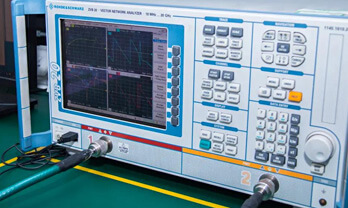
  • Certifications & Memberships

QC (Quality Warranty)

Allelco is committed to exceeding customer expectations through customer service excellence, order accuracy, and on-time delivery.
This is achieved through our commitment to the continual improvement of our processes, services, and products.


Strict quality inspection builds a solid foundation for electronic component quality.
  1. Visual inspection
  2. Performance testing and reliability verification
  3. Standardized full-process testing
  4. Precise control of every parameter
We eliminate defective components and ensure the stable operation of electronic devices through professional quality standards.

Payment Support

The payment method can be chosen from the methods shown below: Wire Transfer (T/T, Bank Transfer), Western Union, Credit card, PayPal.
  • HKBea
  • Paypal
  • MasterCard
  • Western-Union
  • VISA
Stable Delivery, Sincere Partnership — Your Faithful Supply Chain Partner
  • Efficient Supply Management
  • Cost-Saving Procurement
  • Fast Sourcing & Delivery
Contact us if you have any questions.

Packaging

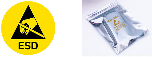
Electrostatic Discharge Protection and Handling

All electrostatic-sensitive components are handled in accordance with electrostatic discharge control procedures. The products are hermetically sealed in anti-static safe packaging to prevent electrostatic damage. Appropriate labeling is also applied for identification and traceability. This ensures product integrity during storage, handling and transportation.


ESD

Certifications & Memberships

Third-party certified, strict quality control. Our certification
  • ISO 9001: 2015
  • ISO 13485: 2016
  • ISO 14001: 2015
  • ISO 28000: 2007
  • ISO 45001: 2018
  • GB/T 27922-2011
  • SMTA
  • IPC
  • ESD
  • PSMA
JST Sales America Inc.

50R-JMDSS-G-1-TF

JST Sales America Inc.
32D-50R-JMDSS-G-1-TF

Want a better price? Add to Cart and Submit RFQ now, we'll contact you immediately.

0 RFQ
Shopping cart (0 Items)
It is empty.
Compare List (0 Items)
It is empty.
Feedback

Your feedback matters! At Allelco, we value the user experience and strive to improve it constantly.
Please share your comments with us via our feedback form, and we'll respond promptly.
Thank you for choosing Allelco.

Subject
E-mail
Comments
Captcha
Drag or click to upload file
Upload File
types: .xls, .xlsx, .doc, .docx, .jpg, .png and .pdf.
Max file size: 10MB