View All

Please refer to the English Version as our Official Version.Return

Europe
France(Français) Germany(Deutsch) Italy(Italia) Russian(русский) Poland(polski) Czech(Čeština) Luxembourg(Lëtzebuergesch) Netherlands(Nederland) Iceland(íslenska) Hungarian(Magyarország) Spain(español) Portugal(Português) Turkey(Türk dili) Bulgaria(Български език) Ukraine(Україна) Greece(Ελλάδα) Israel(עִבְרִית) Sweden(Svenska) Finland(Svenska) Finland(Suomi) Romania(românesc) Moldova(românesc) Slovakia(Slovenská) Denmark(Dansk) Slovenia(Slovenija) Slovenia(Hrvatska) Croatia(Hrvatska) Serbia(Hrvatska) Montenegro(Hrvatska) Bosnia and Herzegovina(Hrvatska) Lithuania(lietuvių) Spain(Português) Switzerland(Deutsch) United Kingdom(English)
Asia/Pacific
Japan(日本語) Korea(한국의) Thailand(ภาษาไทย) Malaysia(Melayu) Singapore(Melayu) Vietnam(Tiếng Việt) Philippines(Pilipino)
Africa, India and Middle East
United Arab Emirates(العربية) Iran(فارسی) Tajikistan(فارسی) India(हिंदी) Madagascar(malaɡasʲ)
South America / Oceania
New Zealand(Maori) Brazil(Português) Angola(Português) Mozambique(Português)
North America
United States(English) Canada(English) Haiti(Ayiti) Mexico(español)
HomeProductsIntegrated Circuits (ICs)Embedded - FPGAs (Field Programmable Gate Array)LCMXO3L-2100E-5MG256C
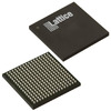
LCMXO3L-2100E-5MG256C Image
Image may be representation.
See specifications for product details.

LCMXO3L-2100E-5MG256C - Lattice Semiconductor Corporation

Manufacturer Part Number
LCMXO3L-2100E-5MG256C
Manufacturer
Lattice Semiconductor
Allelco Part Number
98D-LCMXO3L-2100E-5MG256C
Warranty
1 Year Allelco Warranty - Find out more
Stock Status:
47,141 pcs available, New & Original
Parts Description
IC FPGA 206 I/O 256CSFBGA
Package
256-CSFBGA (9x9)
Data sheet
LCMXO3L-2100E-5.pdf

PCN Packaging

2.73KHz.pdf

PCN Assembly/Origin

2.73KHz.pdf

PCN Design/Specification

Cylindrical Battery Holders.pdf
RoHs Status
ROHS3 Compliant
In stock: 47141
  • Unit Price: $5.717
  • Subtotal: $0.00

Want a better price?
Add to Cart and Submit RFQ now, we'll contact you immediately.

Quantity Unit Price Ext. Price
1+ $5.717 $5.72
260+ $2.213 $575.38
520+ $2.135 $1,110.20
1040+ $2.097 $2,180.88
The above prices does not include taxes and freight rates, which will be calculated on the order pages.


Specifications

LCMXO3L-2100E-5MG256C Tech Specifications
Lattice Semiconductor Corporation - LCMXO3L-2100E-5MG256C technical specifications, attributes, parameters and parts with similar specifications to Lattice Semiconductor Corporation - LCMXO3L-2100E-5MG256C

Product Attribute Attribute Value
Manufacturer Lattice Semiconductor
Voltage - Supply 1.14V ~ 1.26V
Total RAM Bits 75776
Supplier Device Package 256-CSFBGA (9x9)
Series MachXO3
Package / Case 256-VFBGA, CSPBGA
Package Tray
Product Attribute Attribute Value
Operating Temperature 0°C ~ 85°C (TJ)
Number of Logic Elements/Cells 2112
Number of LABs/CLBs 264
Number of I/O 206
Mounting Type Surface Mount
Base Product Number LCMXO3

Environmental & Export Classifications

ATTRIBUTE DESCRIPTION
RoHs Status ROHS3 Compliant
Moisture Sensitivity Level (MSL) 3 (168 Hours)
REACH Status REACH Unaffected
ECCN 3A991D
HTSUS 8542.39.0001

Frequently Asked Questions(FAQ)

What is the typical use case for LCMXO3L-2100E-5MG256C in embedded systems involving I/O expansion and level translation?
The LCMXO3L-2100E-5MG256C is commonly selected in embedded applications where a compact CPLD-style FPGA is needed to bridge between modern low-voltage processors and legacy peripherals. With 206 I/Os and support for multiple I/O standards, it enables implementation of multi-protocol interface logic such as SPI-to-I2C aggregation, GPIO expansion for microcontrollers, or voltage level shifting in space-constrained industrial control boards where full-sized FPGAs would be overkill.
How does the LCMXO3L-2100E-5MG256C compare to Spartan-6 FPGAs in terms of static power consumption for battery-operated equipment?
In portable or energy-sensitive designs, the LCMXO3L-2100E-5MG256C typically exhibits significantly lower static current than comparable Spartan-6 devices, especially at standby. This stems from its 65nm non-volatile flash-based architecture eliminating configuration power drain during operation. For a system requiring persistent configuration without continuous re-load from external memory, the LCMXO3L-2100E-5MG256C offers a more efficient solution with no boot-up delay or external flash interface power overhead.
Can the LCMXO3L-2100E-5MG256C support dual supply operation for interfacing with both 1.2V and 3.3V peripherals in mixed-signal PCBs?
While the LCMXO3L-2100E-5MG256C uses a single core voltage rail (1.14V to 1.26V), its I/O banks can be independently assigned to various voltage standards between 1.2V and 3.3V using external bank supplies. This allows direct interfacing with sensors or communication modules operating at 1.8V, 2.5V, or 3.3V, provided the PCB routes appropriate VCCIO voltages to the relevant pin groups. Designers often leverage this capability when deploying the LCMXO3L-2100E-5MG256C as a protocol translator in modular industrial edge nodes.
What memory architecture is available within LCMXO3L-2100E-5MG256C for implementing FIFOs or state machines?
The LCMXO3L-2100E-5MG256C integrates 75776 total RAM bits distributed across 88 embedded block RAM (EBR) units, each 8192 bits deep. These can be configured as single- or dual-port memories with widths up to 72 bits. In practice, this allows implementation of deep FIFO buffers for data aggregation from ADCs or serial interfaces, or for storing lookup tables in motor control or sensor calibration tasks. For smaller state machines, distributed RAM from the 2112 logic elements may also be used alongside EBR for faster access.
How does the non-volatile configuration of LCMXO3L-2100E-5MG256C impact boot time compared to SRAM-based FPGAs in safety-critical control loops?
Since the LCMXO3L-2100E-5MG256C stores configuration in on-chip flash, it enters user mode immediately on power-up without needing an external configuration PROM. This eliminates the typical 10–100ms configuration phase seen in SRAM-based FPGAs like Cyclone IV or similar, reducing system startup latency. In fast-response applications such as emergency shutdown circuits or real-time monitoring, this behavior supports deterministic operation from initial power application.
What thermal considerations should be evaluated when using LCMXO3L-2100E-5MG256C in densely populated 9x9mm BGA arrays?
The 256-CSFBGA (9x9mm) package of the LCMXO3L-2100E-5MG256C requires careful thermal via placement under the exposed center pad to ensure efficient heat dissipation. At maximum toggle rates and full I/O loading, internal junction temperatures can approach the 85°C upper limit even with moderate ambient conditions. Designers typically allocate at least a 4x4 via array plated to inner ground planes and verify thermal performance using power estimates from Lattice’s Power Calculator based on actual utilization.
How does the logic capacity of LCMXO3L-2100E-5MG256C compare to the EPM240 or ispMACH 4000 in CPLD replacement scenarios?
The LCMXO3L-2100E-5MG256C provides 2112 logic cells and 264 LABs, significantly exceeding the capacity of traditional CPLDs like the EPM240 (240 macrocells) or ispMACH 4000Z (640). This enables consolidation of multiple legacy CPLDs into a single LCMXO3L-2100E-5MG256C device, particularly in designs transitioning from discrete glue logic to programmable control planes. Its non-volatile nature and low static power preserve key CPLD advantages while enabling more complex state machines and data routing.
Is the LCMXO3L-2100E-5MG256C suitable for operating in environments with intermittent temperature cycling between 0°C and 85°C over long durations?
The LCMXO3L-2100E-5MG256C is rated for operation at junction temperatures from 0°C to 85°C, making it appropriate for consumer and industrial equipment exposed to moderate thermal cycling. However, sustained cycling at maximum load may accelerate electromigration effects over time. Long-term reliability is enhanced by adhering to recommended power ramping, maintaining stable I/O voltage supplies, and confirming MSL 3 handling requirements during assembly to avoid moisture-related failures post-reflow.
What debugging and programming interfaces are natively supported by LCMXO3L-2100E-5MG256C during development and field updates?
The LCMXO3L-2100E-5MG256C supports JTAG for boundary-scan testing and direct programming, as well as I2C-based slave mode for field reconfiguration via a host processor. Lattice’s embedded trace capability allows limited internal signal capture without external probes. For in-system updates, the device can use its internal flash-based configuration with secure bitstream storage, enabling field upgrades without exposing configuration data on external memory.
How does the package footprint of LCMXO3L-2100E-5MG256C affect PCB routing complexity in high-density designs?
The 256-CSFBGA package (9x9mm, 1.0mm pitch) of the LCMXO3L-2100E-5MG256C requires microvia or via-in-pad techniques for dense escape routing, particularly with 206 I/Os across four sides. Signal integrity improves when critical high-speed paths are routed on outer layers with controlled impedance, while power and ground networks benefit from dedicated inner planes. Designers often use staggered BGA fanout strategies to minimize crosstalk and reduce layer count in compact IoT or telecom control modules.
What are realistic timing closure expectations for a 100 MHz state machine implemented in LCMXO3L-2100E-5MG256C with full toolchain optimization?
With its 5.0 ns typical input-to-output delay and support for 350 MHz internal clocking under optimal conditions, the LCMXO3L-2100E-5MG256C reliably meets 100 MHz timing targets for moderately complex state machines using Lattice Diamond or Radiant tools. Achieving this depends on proper constraints, pipelining of critical paths, and low-skew clock distribution. Real-world designs such as PCIe endpoint control or camera interface sequencers typically close timing with margin when using embedded DQS for data capture.
Can LCMXO3L-2100E-5MG256C be used as a dedicated SERDES interface for low-pin-count serial protocols?
While the LCMXO3L-2100E-5MG256C lacks dedicated high-speed SERDES transceivers, it can implement up to 4 Gb/s aggregate bandwidth using its programmable I/Os with OSERDES/ISERDES primitives in the logic fabric. This supports custom serialization for display interfaces, memory expansion, or proprietary interconnects up to about 250 Mbps per lane. Applications requiring PCIe or Gigabit Ethernet typically require higher-end MachXO3 devices or alternative FPGAs with hardened PHYs.

Parts with Similar Specifications

The three parts on the right have similar specifications to Lattice Semiconductor Corporation LCMXO3L-2100E-5MG256C

Product Attribute LCMXO3L-2100E-5MG256I LCMXO3L-2100E-5MG121C LCMXO3L-2100E-5MG324C LCMXO3L-2100C-6BG256C
Part Number LCMXO3L-2100E-5MG256I LCMXO3L-2100E-5MG121C LCMXO3L-2100E-5MG324C LCMXO3L-2100C-6BG256C
Manufacturer Lattice Semiconductor Corporation Lattice Semiconductor Corporation Lattice Semiconductor Corporation Lattice Semiconductor Corporation
Supplier Device Package - 196-NFBGA (12x12) 16-PDIP 64-VQFN (9x9)
Mounting Type - Surface Mount Through Hole Surface Mount
Operating Temperature - -40°C ~ 85°C 0°C ~ 70°C -40°C ~ 85°C
Package / Case - 196-LFBGA 16-DIP (0.300', 7.62mm) 64-VFQFN Exposed Pad
Voltage - Supply - - - -
Base Product Number - DAC34H84 MAX500 ADS62P42
Number of LABs/CLBs - - - -
Series - - - -
Number of Logic Elements/Cells - - - -
Total RAM Bits - - - -
Package - Tape & Reel (TR) Tube Tape & Reel (TR)
Number of I/O - - - -

LCMXO3L-2100E-5MG256C Datasheet PDF

Download LCMXO3L-2100E-5MG256C pdf datasheets and Lattice Semiconductor Corporation documentation for LCMXO3L-2100E-5MG256C - Lattice Semiconductor Corporation.

Datasheets
MachXO3 Family Datasheet.pdf
PCN Packaging
2.73KHz.pdf
PCN Assembly/Origin
2.73KHz.pdf
PCN Design/Specification
Cylindrical Battery Holders.pdf

Customer Reviews

Evaluation: 10 Articles

  • Jack***
    Nov 11, 2026

    My order was delivered on time and arrived securely packaged. Communication with the Customer Service team was clear and responsive.

  • Gilb***o Rieck
    Nov 2, 2026

    Communication is always clear, and the team is reliable, helpful, and professional. Everything has gone smoothly, and I really appreciate their commitment to providing great service.

  • Pasc***Elec
    Oct 28, 2026

    The regulator worked properly after assembly, and the output voltage remained steady during basic load testing. The package is quite small, so soldering requires a steady hand and proper equipment. Overall, I'm satisfied with the result.

  • Mark***
    Oct 14, 2026

    We were restoring an automotive control board that uses this Infineon microcontroller. The replacement programmed successfully and communication with the other modules was restored. The repair took some patience, but the component did its job.

  • OldS***olLogic
    Oct 8, 2026

    The CPLD itself works as expected and programmed correctly with our existing setup. It is an older device, so getting the development environment ready took some time, but the hardware has been dependable.

  • Moto***bRavi
    Sep 28, 2026

    This DSP was needed for a legacy motor controller. Programming worked on the first board and speed regulation is operating normally again. Very useful for keeping older equipment running.

  • ECUb***h
    Sep 22, 2026

    Used for repair of an older automotive ECU. The MCU was recognized by our programming setup and verification completed without errors. The repaired board now starts and communicates normally.

  • RS48***ieldTech
    Sep 16, 2026

    Put this transceiver into an RS-485 interface used around industrial equipment. Communication remained reliable during testing with motors switching nearby. Good result for the replacement board.

  • Logi***b_Chris
    Sep 8, 2026

    Purchased for a Cyclone III development project. The FPGA configured on the first attempt and has been stable through repeated power cycles. No problems with the I/O we are using.

  • Circ***FixerTom
    Sep 2, 2026

    Used this rectifier in a high-current power supply repair. Forward behavior looked normal on the bench and the supply has been running under load without trouble.

Write a Review

Your Email address will not be published.

Shipment

Delivery Time

In-stock items can be shipped within 24 hours. Some parts will be arranged for delivery within 1-2 days from the date all items arrive at our warehouse. And Allelco ships order once a day at about 17:00, except Sunday. Once the goods are shipped, the estimated delivery time depends on the shipping methods and Delivery destination. The table below shows are the logistic time for some common countries.

Delivery Cost

  1. Use your express account for shipment if you have one.
  2. Use our account for the shipment. Refer to the table below for the approximate charges.
(Different time frame / countries / package size has different price.)

Delivery Method

  1. Global Common Shipment by DHL / UPS / FedEx / TNT / EMS / SF we support.
  2. Others more shipping ways, please get in touch with your customer manager.

Common Countries Logistic Time Reference
Region Country Logistic Time(Day)
America United States 5
Brazil 7
Europe Germany 5
United Kingdom 4
Italy 5
Oceania Australia 6
New Zealand 5
Asia India 4
Japan 4
Middle East Israel 6
DHL & FedEx Shipment Charges Reference
Shipment charges(KG) Reference DHL(USD$)
0.00kg-1.00kg USD$30.00 - USD$60.00
1.00kg-2.00kg USD$40.00 - USD$80.00
2.00kg-3.00kg USD$50.00 - USD$100.00
Note:
The above table is for reference only. There may have some data bias for the uncontrollable factors.
Contact us if you have any questions.
  • QC (Quality Warranty)
  • Payment Support
  • Packaging

QC (Quality Warranty)

Allelco is committed to exceeding customer expectations through customer service excellence, order accuracy, and on-time delivery.
This is achieved through our commitment to the continual improvement of our processes, services, and products.


Strict quality inspection builds a solid foundation for electronic component quality.
  1. Visual inspection
  2. Performance testing and reliability verification
  3. Standardized full-process testing
  4. Precise control of every parameter
We eliminate defective components and ensure the stable operation of electronic devices through professional quality standards.

Payment Support

The payment method can be chosen from the methods shown below: Wire Transfer (T/T, Bank Transfer), Western Union, Credit card, PayPal.
  • HKBea
  • Paypal
  • MasterCard
  • Western-Union
  • VISA
Stable Delivery, Sincere Partnership — Your Faithful Supply Chain Partner
  • Efficient Supply Management
  • Cost-Saving Procurement
  • Fast Sourcing & Delivery
Contact us if you have any questions.

Packaging

Electrostatic Discharge Protection and Handling

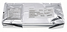
All electrostatic-sensitive components are handled in accordance with electrostatic discharge control procedures. The products are hermetically sealed in anti-static safe packaging to prevent electrostatic damage. Appropriate labeling is also applied for identification and traceability. This ensures product integrity during storage, handling and transportation.


ESD
LCMXO3L-2100E-5MG256C Image

LCMXO3L-2100E-5MG256C

Lattice Semiconductor Corporation
98D-LCMXO3L-2100E-5MG256C

Want a better price? Add to Cart and Submit RFQ now, we'll contact you immediately.

0 RFQ
Shopping cart (0 Items)
It is empty.
Compare List (0 Items)
It is empty.
Feedback

Your feedback matters! At Allelco, we value the user experience and strive to improve it constantly.
Please share your comments with us via our feedback form, and we'll respond promptly.
Thank you for choosing Allelco.

Subject
E-mail
Comments
Captcha
Drag or click to upload file
Upload File
types: .xls, .xlsx, .doc, .docx, .jpg, .png and .pdf.
Max file size: 10MB