View All

Please refer to the English Version as our Official Version.Return

Europe
France(Français) Germany(Deutsch) Italy(Italia) Russian(русский) Poland(polski) Czech(Čeština) Luxembourg(Lëtzebuergesch) Netherlands(Nederland) Iceland(íslenska) Hungarian(Magyarország) Spain(español) Portugal(Português) Turkey(Türk dili) Bulgaria(Български език) Ukraine(Україна) Greece(Ελλάδα) Israel(עִבְרִית) Sweden(Svenska) Finland(Svenska) Finland(Suomi) Romania(românesc) Moldova(românesc) Slovakia(Slovenská) Denmark(Dansk) Slovenia(Slovenija) Slovenia(Hrvatska) Croatia(Hrvatska) Serbia(Hrvatska) Montenegro(Hrvatska) Bosnia and Herzegovina(Hrvatska) Lithuania(lietuvių) Spain(Português) Switzerland(Deutsch) United Kingdom(English)
Asia/Pacific
Japan(日本語) Korea(한국의) Thailand(ภาษาไทย) Malaysia(Melayu) Singapore(Melayu) Vietnam(Tiếng Việt) Philippines(Pilipino)
Africa, India and Middle East
United Arab Emirates(العربية) Iran(فارسی) Tajikistan(فارسی) India(हिंदी) Madagascar(malaɡasʲ)
South America / Oceania
New Zealand(Maori) Brazil(Português) Angola(Português) Mozambique(Português)
North America
United States(English) Canada(English) Haiti(Ayiti) Mexico(español)
HomeProductsIntegrated Circuits (ICs)Embedded - FPGAs (Field Programmable Gate Array)LCMXO3L-2100E-5UWG49ITR
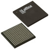
LCMXO3L-2100E-5UWG49ITR Image
Image may be representation.
See specifications for product details.
EXPRESS OPTION
Payment method

LCMXO3L-2100E-5UWG49ITR - Lattice Semiconductor Corporation

Manufacturer Part Number
LCMXO3L-2100E-5UWG49ITR
Manufacturer
Lattice Semiconductor
Allelco Part Number
32D-LCMXO3L-2100E-5UWG49ITR
Warranty
1 Year Allelco Warranty - Find out more
Stock Status:
10,747 pcs available, New & Original
Parts Description
IC FPGA 38 I/O 49WLCSP
Package
49-WLCSP (3.11x3.19)
Data sheet
LCMXO3L-2100E-5.pdf
RoHs Status
ROHS3 Compliant
Our certification
In stock: 10747

Required fields are indicated by an asterisk (*)
Please send RFQ, we will respond immediately.

Quantity

Specifications

LCMXO3L-2100E-5UWG49ITR Tech Specifications
Lattice Semiconductor Corporation - LCMXO3L-2100E-5UWG49ITR technical specifications, attributes, parameters and parts with similar specifications to Lattice Semiconductor Corporation - LCMXO3L-2100E-5UWG49ITR

Product Attribute Attribute Value
Manufacturer Lattice Semiconductor
Voltage - Supply 1.14V ~ 1.26V
Total RAM Bits 75776
Supplier Device Package 49-WLCSP (3.11x3.19)
Series MachXO3
Package / Case 49-UFBGA, WLCSP
Package Tape & Reel (TR)
Product Attribute Attribute Value
Operating Temperature -40°C ~ 100°C (TJ)
Number of Logic Elements/Cells 2112
Number of LABs/CLBs 264
Number of I/O 38
Mounting Type Surface Mount
Base Product Number LCMXO3

Environmental & Export Classifications

ATTRIBUTE DESCRIPTION
RoHs Status ROHS3 Compliant
Moisture Sensitivity Level (MSL) 3 (168 Hours)
REACH Status REACH Unaffected
ECCN EAR99
HTSUS 8542.39.0001

Parts Introduction

LCMXO3L-2100E-5UWG49ITR Image
LCMXO3L-2100E-5UWG49ITR (1)

Manufacturer Part Number

LCMXO3L-2100E-5UWG49ITR

Manufacturer

Lattice Semiconductor

Introduction

The LCMXO3L-2100E-5UWG49ITR is an embedded Field Programmable Gate Array (FPGA) from Lattice Semiconductor, designed for versatility and performance in a wide range of electronic applications.

Product Features and Performance

Utilizes MachXO3 series technology

Contains 264 LABs/CLBs and 2112 Logic Elements/Cells

Features a total of 75776 RAM bits

Equipped with 38 I/Os

Supports supply voltage between 1.14V and 1.26V

Surface mount technology for secure and reliable physical attachment

Operates efficiently within a temperature range of -40°C ~ 100°C (TJ)

Product Advantages

High integration capabilities in a compact 49-WLCSP package (3.11x3.19)

Ensures robust performance even in extreme temperature conditions

Key Technical Parameters

Number of LABs/CLBs: 264

Number of Logic Elements/Cells: 2112

Total RAM Bits: 75776

Number of I/O: 38

Voltage Supply: 1.14V ~ 1.26V

Package / Case: 49-UFBGA, WLCSP

Quality and Safety Features

Robust operational temperature range supporting multiple environments

High quality and reliability standards compliance for safety

Compatibility

Compatible with various design and development tools offered by Lattice and others for FPGA programming and integration

Application Areas

Suitable for consumer electronics, automotive applications, telecommunications, and more

Product Lifecycle

Current product status: Active

Not nearing discontinuation; replacements or upgrades are available if necessary

Several Key Reasons to Choose This Product

Compact packaging with comprehensive logic capabilities

Versatile voltage and temperature range ensuring usability across different platforms and environments

Wide application range supported by dependable manufacturer support and documentation

Continuity assured with no immediate discontinuation and availability of further advancements

Frequently Asked Questions(FAQ)

What are the key architectural advantages of the LCMXO3L-2100E-5UWG49ITR FPGA for low-power embedded control applications?
The LCMXO3L-2100E-5UWG49ITR leverages Lattice’s non-volatile FPGA architecture with instant-on capability, eliminating the need for external configuration memory—critical in power-constrained or space-limited systems. With 2112 logic elements and 75776 bits of embedded RAM distributed across 264 LABs, it provides sufficient resources for implementing glue logic, state machines, and sensor interfacing without requiring a separate microcontroller. Its 1.2V core supply (1.14V–1.26V range) enables ultra-low dynamic power consumption, typically under 100µA in standby, making it suitable for battery-powered edge devices where power efficiency directly impacts operational lifetime.
How does the I/O count and package footprint of the LCMXO3L-2100E-5UWG49ITR influence board-level design decisions in compact industrial systems?
The LCMXO3L-2100E-5UWG49ITR offers 38 user I/Os in a 49-WLCSP package measuring only 3.11 mm × 3.19 mm, enabling high functional density in space-constrained PCBs such as motor drives, HMI panels, or IoT gateways. This small form factor reduces routing complexity and minimizes electromagnetic interference risks by shortening signal paths. However, designers must account for the fine pitch (0.4 mm ball spacing) during layout, requiring precise solder mask definition and reflow profiling to avoid bridging, especially in high-volume manufacturing environments.
Can the LCMXO3L-2100E-5UWG49ITR support real-time communication protocols like SPI or I²C without a soft-core processor?
Yes, the LCMXO3L-2100E-5UWG49ITR can implement SPI and I²C masters or slaves using its programmable logic fabric and hardened sysIO blocks. The device includes dedicated input hysteresis and selectable I/O standards (LVCMOS, LVTTL), allowing robust interfacing with sensors, EEPROMs, or ADCs. For example, a full-duplex SPI controller with clock rates up to 50 MHz can be synthesized within ~150 LEs, leaving ample resources for protocol bridging or data preprocessing—ideal for applications requiring deterministic timing without CPU overhead.
What thermal considerations apply when deploying the LCMXO3L-2100E-5UWG49ITR in an enclosure with limited airflow?
The LCMXO3L-2100E-5UWG49ITR operates from –40°C to 100°C junction temperature, but actual power dissipation must be evaluated under real workloads. In typical glue-logic applications at 25°C ambient, total power remains below 50 mW, minimizing self-heating. However, in sealed enclosures or high-ambient environments (>70°C), thermal resistance from junction to ambient (θJA ≈ 45°C/W in still air) necessitates careful PCB thermal design—such as copper pour under the package and via stitching—to prevent localized hot spots that could degrade timing margins or accelerate aging.
How does the MachXO3 architecture in the LCMXO3L-2100E-5UWG49ITR compare to SRAM-based FPGAs in terms of boot reliability and system startup behavior?
Unlike SRAM-based FPGAs that require external flash to load configuration on power-up, the LCMXO3L-2100E-5UWG49ITR embeds non-volatile configuration storage, enabling true instant-on operation—typically under 1 ms from power application. This eliminates boot sequencing complexity and reduces component count, which is critical in safety-critical systems or those subjected to frequent power cycling. Additionally, the absence of configuration bitstream loading removes vulnerability to single-event upsets (SEUs) in radiation-prone environments, offering inherent reliability over volatile counterparts.
What are the implications of the MSL 3 rating for the LCMXO3L-2100E-5UWG49ITR in high-volume assembly processes?
The moisture sensitivity level (MSL) 3 classification indicates the LCMXO3L-2100E-5UWG49ITR can be exposed to ambient conditions for up to 168 hours after dry packaging is opened before requiring baking. This imposes strict handling protocols in SMT lines: trays or reels must be stored in dry cabinets (<10% RH), and exposure time must be tracked to prevent popcorning during reflow. For high-mix production environments, this may necessitate just-in-time component staging or nitrogen-assisted reflow ovens to mitigate moisture-related defects.
How does the total RAM capacity of the LCMXO3L-2100E-5UWG49ITR influence data buffering strategies in sensor aggregation applications?
With 75,776 bits of distributed block RAM, the LCMXO3L-2100E-5UWG49ITR can implement multiple FIFOs or ping-pong buffers for asynchronous data streams—for instance, buffering 16-bit ADC samples at 1 MSPS for up to 47 µs of latency tolerance. This on-chip memory eliminates the need for external SRAM in moderate-throughput systems, reducing BOM cost and PCB complexity. However, memory access patterns should prioritize localized block usage to minimize routing congestion and maintain timing closure at higher clock frequencies.
What design trade-offs arise when using the LCMXO3L-2100E-5UWG49ITR versus a higher-density FPGA for protocol bridging between legacy and modern interfaces?
While the LCMXO3L-2100E-5UWG49ITR lacks the logic density for complex protocol stacks (e.g., PCIe or Ethernet MAC), its balance of 2112 LEs, 38 I/Os, and low static power makes it ideal for point-to-point bridging tasks such as UART-to-SPI or parallel-to-I²C conversion. Compared to larger FPGAs, it reduces power by an order of magnitude and avoids over-provisioning, but may require external level translators if interfacing with 3.3V peripherals, given its native 1.2V core and I/O voltage constraints.
How does the LCMXO3L-2100E-5UWG49ITR support in-system reprogrammability, and what infrastructure is required on the host PCB?
The LCMXO3L-2100E-5UWG49ITR supports in-system programming via its JTAG or SPI slave interface, allowing firmware updates without removing the device. A minimal 4-wire JTAG header (TCK, TMS, TDI, TDO) or a dedicated SPI flash interface enables field upgrades. However, designers must ensure signal integrity on programming lines—especially in noisy industrial environments—by adding series termination resistors and guarding against ground bounce during concurrent I/O switching.
What verification steps are recommended before committing to the LCMXO3L-2100E-5UWG49ITR in a safety-critical automotive sub-system?
Although the LCMXO3L-2100E-5UWG49ITR is not AEC-Q100 qualified, its –40°C to 100°C operating range and robust I/O protection make it viable for non-safety automotive applications like cabin lighting or infotainment control. Pre-deployment validation should include thermal cycling (–40°C to 125°C), power supply ripple injection testing (±10% on 1.2V rail), and long-duration pattern stress tests to confirm configuration retention and timing stability under environmental extremes.
How does the LCMXO3L-2100E-5UWG49ITR compare to a CPLD for implementing power sequencing logic in a multi-rail system?
The LCMXO3L-2100E-5UWG49ITR offers significantly greater flexibility than traditional CPLDs, with 2112 LEs enabling complex sequencing algorithms, fault detection, and dynamic delay adjustment based on load conditions—features not feasible in fixed-architecture CPLDs. Its non-volatile nature ensures immediate assertion of reset signals on power-up, while the integrated RAM allows logging of fault events. However, for ultra-simple sequencing with <10 states, a CPLD may offer lower unit cost, though at the expense of scalability and debug visibility.
What layout guidelines are critical for achieving signal integrity with the 49-WLCSP package of the LCMXO3L-2100E-5UWG49ITR?
The 0.4 mm ball pitch of the LCMXO3L-2100E-5UWG49ITR demands a microvia-in-pad or laser-drilled via strategy to escape inner signal layers without shorting adjacent balls. Ground and power planes should be solid beneath the package, with decoupling capacitors (100 nF + 1 µF) placed within 2 mm of the supply balls. Differential pairs routed near the FPGA require matched lengths (±5 mil) and reference plane continuity to maintain impedance control, especially when interfacing with high-speed ADCs or communication transceivers.

Parts with Similar Specifications

The three parts on the right have similar specifications to Lattice Semiconductor Corporation LCMXO3L-2100E-5UWG49ITR

Product Attribute LCMXO3L-2100E-5UWG49ITR50 LCMXO3L-2100E-5UWG49ITR1K LCMXO3L-2100E-5UWG49CTR50 LCMXO3L-2100E-5UWG49CTR1K
Part Number LCMXO3L-2100E-5UWG49ITR50 LCMXO3L-2100E-5UWG49ITR1K LCMXO3L-2100E-5UWG49CTR50 LCMXO3L-2100E-5UWG49CTR1K
Manufacturer Lattice Semiconductor Corporation Lattice Semiconductor Corporation Lattice Semiconductor Corporation Lattice Semiconductor Corporation
Number of I/O - - - -
Package - Tape & Reel (TR) Tube Tape & Reel (TR)
Base Product Number - DAC34H84 MAX500 ADS62P42
Mounting Type - Surface Mount Through Hole Surface Mount
Supplier Device Package - 196-NFBGA (12x12) 16-PDIP 64-VQFN (9x9)
Total RAM Bits - - - -
Voltage - Supply - - - -
Number of LABs/CLBs - - - -
Package / Case - 196-LFBGA 16-DIP (0.300', 7.62mm) 64-VFQFN Exposed Pad
Number of Logic Elements/Cells - - - -
Operating Temperature - -40°C ~ 85°C 0°C ~ 70°C -40°C ~ 85°C
Series - - - -

LCMXO3L-2100E-5UWG49ITR Datasheet PDF

Download LCMXO3L-2100E-5UWG49ITR pdf datasheets and Lattice Semiconductor Corporation documentation for LCMXO3L-2100E-5UWG49ITR - Lattice Semiconductor Corporation.

Datasheets
MachXO3 Family Datasheet.pdf
PCN Packaging
All Dev Pkg Mark Chg 12/Nov/2018.pdf
PCN Design/Specification
Datasheet Chg 21/Mar/2016.pdf
PCN Other
I2C Read-Back Failure Feb/2015.pdf
PCN Assembly/Origin
Mult Dev Assembly Chg 13/Jan/2020.pdf
Getting Started Guide
Product Selector Guide.pdf

Customer Reviews

Evaluation: 10 Articles

  • ECUb***h
    Sep 22, 2026

    Used for repair of an older automotive ECU. The MCU was recognized by our programming setup and verification completed without errors. The repaired board now starts and communicates normally.

  • RS48***ieldTech
    Sep 16, 2026

    Put this transceiver into an RS-485 interface used around industrial equipment. Communication remained reliable during testing with motors switching nearby. Good result for the replacement board.

  • Logi***b_Chris
    Sep 8, 2026

    Purchased for a Cyclone III development project. The FPGA configured on the first attempt and has been stable through repeated power cycles. No problems with the I/O we are using.

  • Circ***FixerTom
    Sep 2, 2026

    Used this rectifier in a high-current power supply repair. Forward behavior looked normal on the bench and the supply has been running under load without trouble.

  • Retr***UWorks
    Aug 31, 2026

    Needed the exact ST10F269Z2Q6 for servicing an older control unit. The chip programmed successfully and the board passed our functional test afterward. Much easier than redesigning around a newer MCU.

  • Andr***PCBLab
    Aug 28, 2026

    I needed this ADC for an older data acquisition board. Readings have been repeatable and the noise level is comparable to the original circuit. Happy with the purchase.

  • Leat***O'Keefe
    Aug 20, 2026

    one of my hobbies is skydiving. and when i'm skydiving this works great.

  • Ilen***
    Aug 20, 2026

    This product works considerably well. It secretly improves my basketball by a lot.

  • Indu***ialPower
    Aug 17, 2026

    Installed this IGBT module in a power conversion cabinet. Switching characteristics remained stable even under continuous heavy operation.

  • Nikh***ech
    Aug 13, 2026

    Great low-power MCU for portable equipment. Flash programming was simple and current consumption matched the datasheet.

Write a Review

Your Email address will not be published.

Shipment

Delivery Time

In-stock items can be shipped within 24 hours. Some parts will be arranged for delivery within 1-2 days from the date all items arrive at our warehouse. And Allelco ships order once a day at about 17:00, except Sunday. Once the goods are shipped, the estimated delivery time depends on the shipping methods and Delivery destination. The table below shows are the logistic time for some common countries.

Delivery Cost

  1. Use your express account for shipment if you have one.
  2. Use our account for the shipment. Refer to the table below for the approximate charges.
(Different time frame / countries / package size has different price.)

Delivery Method

  1. Global Common Shipment by DHL / UPS / FedEx / TNT / EMS / SF we support.
  2. Others more shipping ways, please get in touch with your customer manager.

Common Countries Logistic Time Reference
Region Country Logistic Time(Day)
America United States 5
Brazil 7
Europe Germany 5
United Kingdom 4
Italy 5
Oceania Australia 6
New Zealand 5
Asia India 4
Japan 4
Middle East Israel 6
DHL & FedEx Shipment Charges Reference
Shipment charges(KG) Reference DHL(USD$)
0.00kg-1.00kg USD$30.00 - USD$60.00
1.00kg-2.00kg USD$40.00 - USD$80.00
2.00kg-3.00kg USD$50.00 - USD$100.00
Note:
The above table is for reference only. There may have some data bias for the uncontrollable factors.
Contact us if you have any questions.
  • QC (Quality Warranty)
  • Payment Support
  • Packaging
  • Certifications & Memberships

QC (Quality Warranty)

Allelco is committed to exceeding customer expectations through customer service excellence, order accuracy, and on-time delivery.
This is achieved through our commitment to the continual improvement of our processes, services, and products.


Strict quality inspection builds a solid foundation for electronic component quality.
  1. Visual inspection
  2. Performance testing and reliability verification
  3. Standardized full-process testing
  4. Precise control of every parameter
We eliminate defective components and ensure the stable operation of electronic devices through professional quality standards.

Payment Support

The payment method can be chosen from the methods shown below: Wire Transfer (T/T, Bank Transfer), Western Union, Credit card, PayPal.
  • HKBea
  • Paypal
  • MasterCard
  • Western-Union
  • VISA
Stable Delivery, Sincere Partnership — Your Faithful Supply Chain Partner
  • Efficient Supply Management
  • Cost-Saving Procurement
  • Fast Sourcing & Delivery
Contact us if you have any questions.

Packaging

Electrostatic Discharge Protection and Handling

All electrostatic-sensitive components are handled in accordance with electrostatic discharge control procedures. The products are hermetically sealed in anti-static safe packaging to prevent electrostatic damage. Appropriate labeling is also applied for identification and traceability. This ensures product integrity during storage, handling and transportation.


ESD

Certifications & Memberships

Third-party certified, strict quality control. Our certification
  • ISO 9001: 2015
  • ISO 13485: 2016
  • ISO 14001: 2015
  • ISO 28000: 2007
  • ISO 45001: 2018
  • GB/T 27922-2011
  • SMTA
  • IPC
  • ESD
  • PSMA
LCMXO3L-2100E-5UWG49ITR Image

LCMXO3L-2100E-5UWG49ITR

Lattice Semiconductor Corporation
32D-LCMXO3L-2100E-5UWG49ITR

Want a better price? Add to Cart and Submit RFQ now, we'll contact you immediately.

0 RFQ
Shopping cart (0 Items)
It is empty.
Compare List (0 Items)
It is empty.
Feedback

Your feedback matters! At Allelco, we value the user experience and strive to improve it constantly.
Please share your comments with us via our feedback form, and we'll respond promptly.
Thank you for choosing Allelco.

Subject
E-mail
Comments
Captcha
Drag or click to upload file
Upload File
types: .xls, .xlsx, .doc, .docx, .jpg, .png and .pdf.
Max file size: 10MB