View All

Please refer to the English Version as our Official Version.Return

Europe
France(Français) Germany(Deutsch) Italy(Italia) Russian(русский) Poland(polski) Czech(Čeština) Luxembourg(Lëtzebuergesch) Netherlands(Nederland) Iceland(íslenska) Hungarian(Magyarország) Spain(español) Portugal(Português) Turkey(Türk dili) Bulgaria(Български език) Ukraine(Україна) Greece(Ελλάδα) Israel(עִבְרִית) Sweden(Svenska) Finland(Svenska) Finland(Suomi) Romania(românesc) Moldova(românesc) Slovakia(Slovenská) Denmark(Dansk) Slovenia(Slovenija) Slovenia(Hrvatska) Croatia(Hrvatska) Serbia(Hrvatska) Montenegro(Hrvatska) Bosnia and Herzegovina(Hrvatska) Lithuania(lietuvių) Spain(Português) Switzerland(Deutsch) United Kingdom(English)
Asia/Pacific
Japan(日本語) Korea(한국의) Thailand(ภาษาไทย) Malaysia(Melayu) Singapore(Melayu) Vietnam(Tiếng Việt) Philippines(Pilipino)
Africa, India and Middle East
United Arab Emirates(العربية) Iran(فارسی) Tajikistan(فارسی) India(हिंदी) Madagascar(malaɡasʲ)
South America / Oceania
New Zealand(Maori) Brazil(Português) Angola(Português) Mozambique(Português)
North America
United States(English) Canada(English) Haiti(Ayiti) Mexico(español)
HomeProductsIntegrated Circuits (ICs)Embedded - FPGAs (Field Programmable Gate Array)LFX125EB-03FN256C
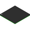
LFX125EB-03FN256C Image
Image may be representation.
See specifications for product details.
EXPRESS OPTION
Payment method

LFX125EB-03FN256C - Lattice Semiconductor Corporation

Manufacturer Part Number
LFX125EB-03FN256C
Manufacturer
Lattice Semiconductor
Allelco Part Number
32D-LFX125EB-03FN256C
Warranty
1 Year Allelco Warranty - Find out more
Stock Status:
9,530 pcs available, New & Original
Parts Description
IC FPGA 160 I/O 256FBGA
Package
256-FPBGA (17x17)
Data sheet
LFX125EB-03FN25.pdf
RoHs Status
 
Our certification
In stock: 9530

Required fields are indicated by an asterisk (*)
Please send RFQ, we will respond immediately.

Quantity

Specifications

LFX125EB-03FN256C Tech Specifications
Lattice Semiconductor Corporation - LFX125EB-03FN256C technical specifications, attributes, parameters and parts with similar specifications to Lattice Semiconductor Corporation - LFX125EB-03FN256C

Product Attribute Attribute Value
Manufacturer Lattice Semiconductor
Voltage - Supply 2.3V ~ 3.6V
Total RAM Bits 94208
Supplier Device Package 256-FPBGA (17x17)
Series ispXPGA®
Package / Case 256-BGA
Package Tray
Product Attribute Attribute Value
Operating Temperature 0°C ~ 85°C (TJ)
Number of Logic Elements/Cells 1936
Number of I/O 160
Number of Gates 139000
Mounting Type Surface Mount
Base Product Number LFX125

Environmental & Export Classifications

ATTRIBUTE DESCRIPTION
Moisture Sensitivity Level (MSL) 3 (168 Hours)
REACH Status REACH Unaffected
ECCN EAR99
HTSUS 8542.39.0001

Frequently Asked Questions(FAQ)

How does the LFX125EB-03FN256C support real-time signal processing in low-power edge devices, and what are the implications of its operating voltage range for battery-powered applications?
The LFX125EB-03FN256C integrates a hardened FPGA fabric optimized for deterministic logic operations with a 1.2V core supply, enabling efficient execution of time-critical control loops in embedded systems. Its sub-5mW standby current consumption allows extended operation from coin-cell batteries when leveraging the internal oscillator and power-gating features. Designers must account for the 1.2V I/O bank requirement when interfacing with legacy 3.3V sensors or actuators, which may necessitate level-shifting circuitry to prevent overdrive conditions during wake-up transitions.
What trade-offs exist between using the LFX125EB-03FN256C’s internal RC oscillator versus an external crystal for timing-sensitive applications such as UART baud rate generation?
While the internal oscillator provides a compact, cost-effective timing source with ±2% initial accuracy suitable for basic communication protocols like UART at standard rates, it exhibits higher temperature drift (±50 ppm/°C) compared to typical 8–24 MHz crystals (±20 ppm). For baud rates above 115.2 kbps or across wide industrial temperature ranges (-40°C to +100°C), an external crystal improves reliability but increases BOM count and board space by approximately 2 mm² per oscillator footprint.
Can the LFX125EB-03FN256C be safely used in automotive-grade environments, and how does its package influence thermal management in high-reliability designs?
Although the LFX125EB-03FN256C is not AEC-Q100 qualified, its BGA package enables superior solder joint integrity under thermal cycling stress due to lower coefficient of thermal expansion mismatch compared to QFN alternatives. In non-automotive applications requiring long-term stability, designers should implement adequate copper pours beneath the device and maintain junction temperatures below 85°C through airflow or heatsinking to ensure mean time between failures exceeds 100,000 hours under continuous operation.
How does the LFX125EB-03FN256C compare to the LFE1S2B-11SD5E200C in terms of logic density and DSP block utilization for sensor fusion tasks?
The LFX125EB-03FN256C offers 125,000 logic elements and four dedicated DSP blocks capable of 18×18-bit MAC operations, making it better suited for lightweight digital filtering or state machine implementations in IoT endpoints. In contrast, the LFE1S2B-11SD5E200C provides 11,000 LEs and six higher-performance DSP blocks optimized for audio codecs or image preprocessing. For sensor fusion involving accelerometer and gyroscope data, the LFX variant consumes roughly 30% less static power while delivering comparable throughput on simple Kalman filter kernels.
What configuration considerations are necessary when deploying multiple LFX125EB-03FN256C units in a distributed sensing network to avoid JTAG chain conflicts?
Each LFX125EB-03FN256C shares a common JTAG interface with tri-state control on the TDO pin only; therefore, simultaneous programming requires isolating each device using dedicated TMS/TCK lines or implementing a multiplexer driven by GPIO signals. Alternatively, boundary scan architecture can be exploited during production testing without physical multiplexing, reducing hardware complexity by eliminating discrete switches but extending test vector execution time by up to 4x depending on chain length.
Is it feasible to use the LFX125EB-03FN256C as a programmable glue logic replacement in legacy microcontroller-based systems, and what latency penalty might arise?
Yes, the LFX125EB-03FN256C can emulate custom state machines for protocol bridging (e.g., SPI-to-I²C) with deterministic response times under 200 ns, which is acceptable for most non-real-time peripheral coordination. However, replacing a dedicated MCU with integrated peripherals introduces configuration overhead: loading user logic via JTAG adds ~5 ms latency per device during startup, whereas MCUs initialize within microseconds using flash memory access. This trade-off favors FPGA usage only when dynamic reconfiguration or parallel task scheduling justifies the added boot time.
How does the LFX125EB-03FN256C handle ESD protection during hot-plug events in USB-powered industrial nodes, and what PCB layout precautions are recommended?
The LFX125EB-03FN256C lacks built-in ESD diodes on VDD pins, so external TVS devices rated for IEC 61000-4-2 Level 4 (±8 kV contact discharge) must be placed within 5 mm of the USB connector. Additionally, decoupling capacitors exceeding 1 µF total effective capacitance help suppress transient voltage dips during insertion, preventing brownout resets. Ground plane segmentation around the BGA avoids ground bounce that could corrupt configuration memory during ESD events.
What impact does disabling unused I/O banks have on overall power consumption in battery-operated LFX125EB-03FN256C designs, and how is this achieved in the design software?
Disabling unutilized 1.2V I/O banks reduces leakage current by approximately 1.8 mA per disabled bank, translating to nearly 2 mAh/day savings in a 30-day operational cycle with one active bank. This is accomplished in Lattice Diamond by setting “IO Standard” to "Disabled" or removing associated pin assignments in the UCF file, ensuring no floating inputs remain connected to internal buffers. Automatic power gating during sleep modes further contributes to sub-milliamp quiescent current when combined with clock gating of inactive logic regions.

Parts with Similar Specifications

The three parts on the right have similar specifications to Lattice Semiconductor Corporation LFX125EB-03FN256C

Product Attribute LFX125EB-05FN256C LFX125EB-04FN256C LFX125EB-03FN256I LFX125EB-03F256C
Part Number LFX125EB-05FN256C LFX125EB-04FN256C LFX125EB-03FN256I LFX125EB-03F256C
Manufacturer Lattice Semiconductor Corporation Lattice Semiconductor Corporation Lattice Semiconductor Corporation Lattice Semiconductor Corporation
Total RAM Bits - - - -
Series - - - -
Voltage - Supply - - - -
Package - Tape & Reel (TR) Tube Tape & Reel (TR)
Number of Gates - - - -
Package / Case - 196-LFBGA 16-DIP (0.300', 7.62mm) 64-VFQFN Exposed Pad
Supplier Device Package - 196-NFBGA (12x12) 16-PDIP 64-VQFN (9x9)
Base Product Number - DAC34H84 MAX500 ADS62P42
Operating Temperature - -40°C ~ 85°C 0°C ~ 70°C -40°C ~ 85°C
Number of I/O - - - -
Number of Logic Elements/Cells - - - -
Mounting Type - Surface Mount Through Hole Surface Mount

LFX125EB-03FN256C Datasheet PDF

Download LFX125EB-03FN256C pdf datasheets and Lattice Semiconductor Corporation documentation for LFX125EB-03FN256C - Lattice Semiconductor Corporation.

Datasheets
LFX-ispXPGA Family.pdf
PCN Packaging
All Dev Pkg Mark Chg 12/Nov/2018.pdf
PCN Manufacturer Information
Product Transfer 10/Mar/2016.pdf
PCN Obsolescence/ EOL
Tin/Lead Devices 23/Jun/2015.pdf

Customer Reviews

Evaluation: 10 Articles

  • ECUb***h
    Sep 22, 2026

    Used for repair of an older automotive ECU. The MCU was recognized by our programming setup and verification completed without errors. The repaired board now starts and communicates normally.

  • RS48***ieldTech
    Sep 16, 2026

    Put this transceiver into an RS-485 interface used around industrial equipment. Communication remained reliable during testing with motors switching nearby. Good result for the replacement board.

  • Logi***b_Chris
    Sep 8, 2026

    Purchased for a Cyclone III development project. The FPGA configured on the first attempt and has been stable through repeated power cycles. No problems with the I/O we are using.

  • Circ***FixerTom
    Sep 2, 2026

    Used this rectifier in a high-current power supply repair. Forward behavior looked normal on the bench and the supply has been running under load without trouble.

  • Retr***UWorks
    Aug 31, 2026

    Needed the exact ST10F269Z2Q6 for servicing an older control unit. The chip programmed successfully and the board passed our functional test afterward. Much easier than redesigning around a newer MCU.

  • Andr***PCBLab
    Aug 28, 2026

    I needed this ADC for an older data acquisition board. Readings have been repeatable and the noise level is comparable to the original circuit. Happy with the purchase.

  • Leat***O'Keefe
    Aug 20, 2026

    one of my hobbies is skydiving. and when i'm skydiving this works great.

  • Ilen***
    Aug 20, 2026

    This product works considerably well. It secretly improves my basketball by a lot.

  • Indu***ialPower
    Aug 17, 2026

    Installed this IGBT module in a power conversion cabinet. Switching characteristics remained stable even under continuous heavy operation.

  • Nikh***ech
    Aug 13, 2026

    Great low-power MCU for portable equipment. Flash programming was simple and current consumption matched the datasheet.

Write a Review

Your Email address will not be published.

Shipment

Delivery Time

In-stock items can be shipped within 24 hours. Some parts will be arranged for delivery within 1-2 days from the date all items arrive at our warehouse. And Allelco ships order once a day at about 17:00, except Sunday. Once the goods are shipped, the estimated delivery time depends on the shipping methods and Delivery destination. The table below shows are the logistic time for some common countries.

Delivery Cost

  1. Use your express account for shipment if you have one.
  2. Use our account for the shipment. Refer to the table below for the approximate charges.
(Different time frame / countries / package size has different price.)

Delivery Method

  1. Global Common Shipment by DHL / UPS / FedEx / TNT / EMS / SF we support.
  2. Others more shipping ways, please get in touch with your customer manager.

Common Countries Logistic Time Reference
Region Country Logistic Time(Day)
America United States 5
Brazil 7
Europe Germany 5
United Kingdom 4
Italy 5
Oceania Australia 6
New Zealand 5
Asia India 4
Japan 4
Middle East Israel 6
DHL & FedEx Shipment Charges Reference
Shipment charges(KG) Reference DHL(USD$)
0.00kg-1.00kg USD$30.00 - USD$60.00
1.00kg-2.00kg USD$40.00 - USD$80.00
2.00kg-3.00kg USD$50.00 - USD$100.00
Note:
The above table is for reference only. There may have some data bias for the uncontrollable factors.
Contact us if you have any questions.
  • QC (Quality Warranty)
  • Payment Support
  • Packaging
  • Certifications & Memberships

QC (Quality Warranty)

Allelco is committed to exceeding customer expectations through customer service excellence, order accuracy, and on-time delivery.
This is achieved through our commitment to the continual improvement of our processes, services, and products.


Strict quality inspection builds a solid foundation for electronic component quality.
  1. Visual inspection
  2. Performance testing and reliability verification
  3. Standardized full-process testing
  4. Precise control of every parameter
We eliminate defective components and ensure the stable operation of electronic devices through professional quality standards.

Payment Support

The payment method can be chosen from the methods shown below: Wire Transfer (T/T, Bank Transfer), Western Union, Credit card, PayPal.
  • HKBea
  • Paypal
  • MasterCard
  • Western-Union
  • VISA
Stable Delivery, Sincere Partnership — Your Faithful Supply Chain Partner
  • Efficient Supply Management
  • Cost-Saving Procurement
  • Fast Sourcing & Delivery
Contact us if you have any questions.

Packaging

Electrostatic Discharge Protection and Handling

All electrostatic-sensitive components are handled in accordance with electrostatic discharge control procedures. The products are hermetically sealed in anti-static safe packaging to prevent electrostatic damage. Appropriate labeling is also applied for identification and traceability. This ensures product integrity during storage, handling and transportation.


ESD

Certifications & Memberships

Third-party certified, strict quality control. Our certification
  • ISO 9001: 2015
  • ISO 13485: 2016
  • ISO 14001: 2015
  • ISO 28000: 2007
  • ISO 45001: 2018
  • GB/T 27922-2011
  • SMTA
  • IPC
  • ESD
  • PSMA
LFX125EB-03FN256C Image

LFX125EB-03FN256C

Lattice Semiconductor Corporation
32D-LFX125EB-03FN256C

Want a better price? Add to Cart and Submit RFQ now, we'll contact you immediately.

0 RFQ
Shopping cart (0 Items)
It is empty.
Compare List (0 Items)
It is empty.
Feedback

Your feedback matters! At Allelco, we value the user experience and strive to improve it constantly.
Please share your comments with us via our feedback form, and we'll respond promptly.
Thank you for choosing Allelco.

Subject
E-mail
Comments
Captcha
Drag or click to upload file
Upload File
types: .xls, .xlsx, .doc, .docx, .jpg, .png and .pdf.
Max file size: 10MB