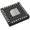
View All

Please refer to the English Version as our Official Version.Return

Europe
France(Français) Germany(Deutsch) Italy(Italia) Russian(русский) Poland(polski) Czech(Čeština) Luxembourg(Lëtzebuergesch) Netherlands(Nederland) Iceland(íslenska) Hungarian(Magyarország) Spain(español) Portugal(Português) Turkey(Türk dili) Bulgaria(Български език) Ukraine(Україна) Greece(Ελλάδα) Israel(עִבְרִית) Sweden(Svenska) Finland(Svenska) Finland(Suomi) Romania(românesc) Moldova(românesc) Slovakia(Slovenská) Denmark(Dansk) Slovenia(Slovenija) Slovenia(Hrvatska) Croatia(Hrvatska) Serbia(Hrvatska) Montenegro(Hrvatska) Bosnia and Herzegovina(Hrvatska) Lithuania(lietuvių) Spain(Português) Switzerland(Deutsch) United Kingdom(English)
Asia/Pacific
Japan(日本語) Korea(한국의) Thailand(ภาษาไทย) Malaysia(Melayu) Singapore(Melayu) Vietnam(Tiếng Việt) Philippines(Pilipino)
Africa, India and Middle East
United Arab Emirates(العربية) Iran(فارسی) Tajikistan(فارسی) India(हिंदी) Madagascar(malaɡasʲ)
South America / Oceania
New Zealand(Maori) Brazil(Português) Angola(Português) Mozambique(Português)
North America
United States(English) Canada(English) Haiti(Ayiti) Mexico(español)
HomeProductsIntegrated Circuits (ICs)Data Acquisition - Analog to Digital Converters (ADC)ADS1261BIRHBR
ADS1261BIRHBR Image
Image may be representation.
See specifications for product details.
EXPRESS OPTION
Payment method

ADS1261BIRHBR - Texas Instruments

Manufacturer Part Number
ADS1261BIRHBR
Manufacturer
Texas Instruments
Allelco Part Number
32D-ADS1261BIRHBR
Warranty
1 Year Allelco Warranty - Find out more
Stock Status:
3,483 pcs available, New & Original
Parts Description
IC ADC 24BIT SIGMA-DELTA 32VQFN
Package
32-VQFN (5x5)
Data sheet
ADS1261BIRHBR.pdf
RoHs Status
ROHS3 Compliant
Our certification
In stock: 3483
  • Unit Price: $13.20
  • Subtotal: $0.00

Want a better price?
Add to Cart and Submit RFQ now, we'll contact you immediately.

Quantity Unit Price Ext. Price
1+ $13.20 $13.20
30+ $12.68 $380.40
The above prices does not include taxes and freight rates, which will be calculated on the order pages.

Specifications

ADS1261BIRHBR Tech Specifications
Texas Instruments - ADS1261BIRHBR technical specifications, attributes, parameters and parts with similar specifications to Texas Instruments - ADS1261BIRHBR

Product Attribute Attribute Value
Manufacturer Texas Instruments
Voltage - Supply, Digital 2.7V ~ 5.25V
Voltage - Supply, Analog 4.75V ~ 5.25V
Supplier Device Package 32-VQFN (5x5)
Series -
Sampling Rate (Per Second) 40k
Reference Type External, Internal
Ratio - S/H:ADC -
Package / Case 32-VFQFN Exposed Pad
Package Tape & Reel (TR)
Operating Temperature -40°C ~ 125°C
Product Attribute Attribute Value
Number of Inputs 10
Number of Bits 24
Number of A/D Converters 1
Mounting Type Surface Mount
Input Type Differential, Single Ended
Features PGA
Data Interface SPI
Configuration MUX-PGA-ADC
Base Product Number ADS1261
Architecture Sigma-Delta

Environmental & Export Classifications

ATTRIBUTE DESCRIPTION
RoHs Status ROHS3 Compliant
Moisture Sensitivity Level (MSL) 3 (168 Hours)
REACH Status REACH Unaffected
ECCN EAR99
HTSUS 8542.39.0001

Parts Introduction

ADS1261BIRHBR Image
ADS1261BIRHBR (1)

Manufacturer Part Number

ADS1261BIRHBR

Manufacturer

Texas Instruments

Introduction

ADS1261BIRHBR is a 24-bit, high-precision sigma-delta ADC with a configurable data acquisition system.

Product Features and Performance

High resolution 24-bit ADC

Sampling Rate up to 40k Samples Per Second

10 Input Channels

Supports Both Differential and Single-Ended Inputs

SPI Data Interface for Communication

Integrated MUX, PGA, and ADC Configuration

Programmable Gain Amplifier for Signal Conditioning

Sigma-Delta Architecture for High Fidelity Data Conversion

Dual Voltage Supply Support for Analog and Digital Operations

Internal and External Reference Voltage Options

Operating Temperature Range from -40°C to 125°C

Product Advantages

High precision measurement capabilities

Flexible input configurations to accommodate various signal types

Compact 32-VFQFN Exposed Pad package suitable for space-constrained applications

On-chip features minimize external components required

Robust performance over a wide temperature range

Key Technical Parameters

Number of Bits: 24

Sampling Rate: 40k SPS

Number of Inputs: 10

Input Type: Differential, Single Ended

Data Interface: SPI

Voltage Supply, Analog: 4.75V to 5.25V

Voltage Supply, Digital: 2.7V to 5.25V

Package / Case: 32-VFQFN Exposed Pad

Quality and Safety Features

Extended temperature range operation for industrial environments

Precision data conversion for reliable measurements

Quality packaging compatible with standard SMT assembly

Compatibility

SPI compatible interface for easy integration with most microcontrollers

Flexible voltage range accommodating mixed-voltage systems design

Application Areas

Industrial data acquisition systems

Medical instrumentation

Test and measurement equipment

Process control

Portable instrumentation

Product Lifecycle

Product Status: Active

Not nearing discontinuation

Availability of replacements or upgrades typically through same manufacturer product lines

Several Key Reasons to Choose This Product

High resolution and accurate data conversion for precise applications

Multi-channel input with high sampling rate facilitates complex measurements

Integrated features such as PGA reduce system design complexity

Robust performance characteristics suitable for harsh industrial environments

Supported by Texas Instruments' reputation for quality and long-term availability

Frequently Asked Questions(FAQ)

How does the ADS1261BIRHBR’s 24-bit resolution and 40kSPS sampling rate compare to typical 16-bit ADCs in industrial sensor measurement applications, particularly when measuring low-level signals with high noise sensitivity?
The ADS1261BIRHBR offers a 24-bit sigma-delta architecture that provides significantly higher resolution than conventional 16-bit ADCs, resulting in a dynamic range of over 140 dB under optimal conditions. This enables detection of microvolt-level changes in sensor output, which is essential for precision measurements such as strain gauge or thermocouple readings. While 16-bit ADCs typically achieve around 96 dB SNR, the ADS1261BIRHBR achieves up to 135 dB SNR due to its integrated programmable gain amplifier (PGA) and oversampling architecture. At 40kSPS, it balances speed with effective noise reduction through digital filtering, making it suitable for applications requiring both high fidelity and moderate update rates without sacrificing signal integrity.
What design considerations are critical when interfacing the ADS1261BIRHBR with a microcontroller via SPI, especially regarding clock synchronization and data frame handling?
The ADS1261BIRHBR uses a standard SPI interface operating at up to 20 MHz, but proper timing alignment between the DRDY (data ready) signal and the SPI clock is crucial to avoid data corruption. Since the device generates an asynchronous DRDY pulse when new conversion data is available, the microcontroller must poll this pin or use interrupt-driven reads to ensure accurate sample capture. Additionally, the 32-bit conversion result must be read in sequence across four bytes, and care should be taken to maintain consistent byte order (MSB-first) and handle potential timing gaps between read operations. Failure to align these elements can lead to stale or misaligned data samples, degrading measurement accuracy.
Can the ADS1261BIRHBR simultaneously measure multiple differential inputs using its internal multiplexer, and how does channel switching affect settling time and measurement latency?
Yes, the ADS1261BIRHBR supports sequential scanning of all 10 input channels via its internal MUX-PGA-ADC configuration. However, channel switching introduces a finite settling time dictated by the selected PGA gain setting—higher gains increase settling requirements. For example, with a gain of 128, the device requires approximately 3.75 µs for the PGA to stabilize after a channel change, during which time the ADC cannot accept valid conversions. This results in a total conversion cycle time of about 25 µs per channel at 40kSPS, limiting true simultaneous sampling but enabling multiplexed scanning at up to 400 kSPS aggregate throughput across all channels when properly managed.
In what scenarios would using an external reference voltage be preferable over the internal reference of the ADS1261BIRHBR, and how does reference stability impact long-term measurement drift?
An external reference, such as a precision bandgap source like the REF5050, is recommended when absolute accuracy and long-term stability are required over wide temperature ranges or extended operational lifetimes. The ADS1261BIRHBR’s internal reference has a typical accuracy of ±0.05% but may exhibit temperature drift of ±10 ppm/°C, leading to cumulative errors in high-resolution applications. In contrast, low-drift external references can achieve ±25 ppm/°C or better, reducing total system error budget. For battery-powered or remote monitoring systems where recalibration is impractical, an external reference improves traceability to national standards and minimizes voltage-induced gain errors, especially when paired with the device’s PGA settings exceeding 128x.
How does the power supply sequencing requirement for the ADS1261BIRHBR affect system-level design, particularly when analog and digital supplies are derived from different regulators?
The ADS1261BIRHBR allows independent analog (AVDD = 4.75V–5.25V) and digital (DVDD = 2.7V–5.25V) supply rails, offering flexibility in mixed-signal power architectures. However, both supplies must be active before asserting the RESET pin and remain stable throughout operation to prevent latch-up or undefined logic states. Although there is no strict sequencing requirement per datasheet, best practice dictates that DVDD should reach nominal levels first to ensure clean digital initialization, followed shortly by AVDD to allow analog circuitry stabilization. Skipping this coordination may cause erratic behavior during startup, including false DRDY pulses or incorrect register reads, complicating debug cycles in embedded firmware.
What are the key differences between using single-ended versus differential input configurations with the ADS1261BIRHBR, and how do they affect common-mode rejection and noise immunity in noisy industrial environments?
Differential inputs on the ADS1261BIRHBR provide superior noise rejection compared to single-ended modes by rejecting signals common to both input pins. This makes differential mode ideal for transducer bridges or long cable runs subject to electromagnetic interference (EMI). In single-ended mode, one input connects to ground or a fixed bias, increasing susceptibility to ground loops and common-mode voltages. The device achieves >100 dB CMRR at DC with appropriate PGA gain, but performance degrades slightly at higher frequencies. For applications involving floating sources or unbalanced transmission lines, differential pairing preserves signal integrity, whereas single-ended usage demands careful layout and shielding to maintain effective resolution, especially at lower gain settings where noise dominates the signal path.
When selecting a PCB layout strategy for the ADS1261BIRHBR in a 32-VQFN package, what routing and grounding practices are necessary to preserve ADC performance and minimize crosstalk?
To maintain the ADS1261BIRHBR’s high resolution, the analog ground (AGND) must be isolated from digital grounds (DGND) and connected to the PGND plane only at a single point near the device’s exposed thermal pad. Power traces should be short and direct, with decoupling capacitors (e.g., 10 µF tantalum + 0.1 µF ceramic) placed within 2 mm of the VDD pins. Signal traces routed to the 10 input channels must avoid crossing digital clock lines or high-current paths to prevent capacitive coupling. The thermal pad requires multiple vias to inner layer ground planes to ensure low-impedance heat dissipation and electrical continuity. Poor grounding or shared return paths introduce ground bounce, degrading ENOB (effective number of bits) and increasing harmonic distortion, particularly noticeable at higher PGA gains and full-scale inputs.
How does temperature variation from -40°C to 125°C affect the offset and gain error of the ADS1261BIRHBR, and what compensation techniques are commonly employed in precision measurement systems?
Over the full operating temperature range, the ADS1261BIRHBR exhibits typical offset drift of ±1 µV/°C and gain drift of ±5 ppm/°C when using the internal reference. These drifts translate into significant output errors in high-gain configurations; for instance, at 128x PGA, a 50°C swing could induce up to 2.5 mV error in a 5V full-scale system. To mitigate this, many designs implement periodic zero-scale and full-scale calibration routines using internal test signals (e.g., short-circuit and open-circuit inputs), or rely on external temperature sensors to apply lookup-table corrections in firmware. Alternatively, pairing the device with a low-drift external reference further reduces thermal dependency. Without such compensation, long-term stability in harsh environments falls below 0.01%, limiting suitability for metrology or calibration-grade instrumentation.

Parts with Similar Specifications

The three parts on the right have similar specifications to Texas Instruments ADS1261BIRHBR

Product Attribute ADS1260BIRHBR ADS1261BQWRHMRQ1 ADS125H01IRHBT ADS125H02IRHBR
Part Number ADS1260BIRHBR ADS1261BQWRHMRQ1 ADS125H01IRHBT ADS125H02IRHBR
Manufacturer Texas Instruments Texas Instruments Texas Instruments Texas Instruments
Base Product Number - DAC34H84 MAX500 ADS62P42
Series - - - -
Sampling Rate (Per Second) - - - 65M
Architecture - Current Source R-2R Pipelined
Data Interface - LVDS - Parallel I²C LVDS - Parallel, Parallel
Voltage - Supply, Analog - 3.14V ~ 3.46V 11.4V ~ 16.5V 3V ~ 3.6V
Package - Tape & Reel (TR) Tube Tape & Reel (TR)
Operating Temperature - -40°C ~ 85°C 0°C ~ 70°C -40°C ~ 85°C
Configuration - - - S/H-ADC
Package / Case - 196-LFBGA 16-DIP (0.300', 7.62mm) 64-VFQFN Exposed Pad
Mounting Type - Surface Mount Through Hole Surface Mount
Number of Inputs - - - 2
Features - - - Simultaneous Sampling
Number of Bits - 16 8 14
Input Type - - - Differential
Number of A/D Converters - - - 2
Supplier Device Package - 196-NFBGA (12x12) 16-PDIP 64-VQFN (9x9)
Reference Type - External, Internal External External, Internal
Voltage - Supply, Digital - 1.14V ~ 1.26V 11.4V ~ 16.5V 1.65V ~ 3.6V
Ratio - S/H:ADC - - - 1:1

ADS1261BIRHBR Datasheet PDF

Download ADS1261BIRHBR pdf datasheets and Texas Instruments documentation for ADS1261BIRHBR - Texas Instruments.

HTML Datasheet
ADS1260, ADS1261 Datasheet.pdf

Customer Reviews

Evaluation: 10 Articles

  • Dani***alkerTech
    Jun 1, 2026

    Product works, but setup took more effort than expected. Once configured the MCU ran reliably, although documentation support felt older compared with newer platforms. Fine for maintenance projects.

  • Yuki***aka88
    May 26, 2026

    信号通信プロジェクトでこのRS-485トランシーバーを使用しました。設置は簡単で、長距離ケーブルでも通信は安定していました。消費電力も、以前使用していたものより低くなっています。

  • Stev***aker
    May 20, 2026

    Solid diode for power rectification. Works well in switching circuits.

  • Bran***Lewis
    May 11, 2026

    Compact FPGA with good performance. Suitable for basic signal processing tasks.

  • Oliv***arris
    May 7, 2026

    Reliable I/O expander. Works well in embedded control applications.

  • Jess***Jones
    Apr 17, 2026

    It offers good value for the price, and the specifications match the description. I’ve been using it for two days with no issues, and I’ll definitely buy it again if I need it in the future.

  • Mich***Smith
    Apr 17, 2026

    Shipping was on time, the component pins are neatly aligned, and I tested 10 of them with a multimeter—all readings were within the specified range. Highly recommended.

  • Aman***arris
    Apr 3, 2026

    It was great—the entire process, from placing the order to receiving the package, went very smoothly. The components were consistent, the price was fair, and I had a very pleasant shopping experience.

  • Mike***nch
    Apr 3, 2026

    Better than expected! The resistance and capacitance readings were spot-on, and it passed the test on the first try. The service was reliable, and the packaging was thoughtful—I highly recommend it.

  • Daic***K.
    Mar 23, 2026

    Very good. No issue after long time testing.

Write a Review

Your Email address will not be published.

Shipment

Delivery Time

In-stock items can be shipped within 24 hours. Some parts will be arranged for delivery within 1-2 days from the date all items arrive at our warehouse. And Allelco ships order once a day at about 17:00, except Sunday. Once the goods are shipped, the estimated delivery time depends on the shipping methods and Delivery destination. The table below shows are the logistic time for some common countries.

Delivery Cost

  1. Use your express account for shipment if you have one.
  2. Use our account for the shipment. Refer to the table below for the approximate charges.
(Different time frame / countries / package size has different price.)

Delivery Method

  1. Global Common Shipment by DHL / UPS / FedEx / TNT / EMS / SF we support.
  2. Others more shipping ways, please get in touch with your customer manager.

Common Countries Logistic Time Reference
Region Country Logistic Time(Day)
America United States 5
Brazil 7
Europe Germany 5
United Kingdom 4
Italy 5
Oceania Australia 6
New Zealand 5
Asia India 4
Japan 4
Middle East Israel 6
DHL & FedEx Shipment Charges Reference
Shipment charges(KG) Reference DHL(USD$)
0.00kg-1.00kg USD$30.00 - USD$60.00
1.00kg-2.00kg USD$40.00 - USD$80.00
2.00kg-3.00kg USD$50.00 - USD$100.00
Note:
The above table is for reference only. There may have some data bias for the uncontrollable factors.
Contact us if you have any questions.
  • QC (Quality Warranty)
  • Payment Support
  • Packaging
  • Certifications & Memberships

QC (Quality Warranty)

Allelco is committed to exceeding customer expectations through customer service excellence, order accuracy, and on-time delivery.
This is achieved through our commitment to the continual improvement of our processes, services, and products.


Strict quality inspection builds a solid foundation for electronic component quality.
  1. Visual inspection
  2. Performance testing and reliability verification
  3. Standardized full-process testing
  4. Precise control of every parameter
We eliminate defective components and ensure the stable operation of electronic devices through professional quality standards.

Payment Support

The payment method can be chosen from the methods shown below: Wire Transfer (T/T, Bank Transfer), Western Union, Credit card, PayPal.
  • HKBea
  • Paypal
  • MasterCard
  • Western-Union
  • VISA
Stable Delivery, Sincere Partnership — Your Faithful Supply Chain Partner
  • Efficient Supply Management
  • Cost-Saving Procurement
  • Fast Sourcing & Delivery
Contact us if you have any questions.

Packaging

Electrostatic Discharge Protection and Handling

All electrostatic-sensitive components are handled in accordance with electrostatic discharge control procedures. The products are hermetically sealed in anti-static safe packaging to prevent electrostatic damage. Appropriate labeling is also applied for identification and traceability. This ensures product integrity during storage, handling and transportation.


ESD

Certifications & Memberships

Third-party certified, strict quality control. Our certification
  • ISO 9001: 2015
  • ISO 13485: 2016
  • ISO 14001: 2015
  • ISO 28000: 2007
  • ISO 45001: 2018
  • GB/T 27922-2011
  • SMTA
  • IPC
  • ESD
  • PSMA
ADS1261BIRHBR Image

ADS1261BIRHBR

Texas Instruments
32D-ADS1261BIRHBR

Want a better price? Add to Cart and Submit RFQ now, we'll contact you immediately.

0 RFQ
Shopping cart (0 Items)
It is empty.
Compare List (0 Items)
It is empty.
Feedback

Your feedback matters! At Allelco, we value the user experience and strive to improve it constantly.
Please share your comments with us via our feedback form, and we'll respond promptly.
Thank you for choosing Allelco.

Subject
E-mail
Comments
Captcha
Drag or click to upload file
Upload File
types: .xls, .xlsx, .doc, .docx, .jpg, .png and .pdf.
Max file size: 10MB