OPA2320AIDRGT (1)
Manufacturer Part Number
OPA2320AIDRGT
Manufacturer
Texas Instruments
Introduction
Dual-channel operational amplifier (op-amp) integrated circuit (IC)
Designed for precision instrumentation and control applications
Product Features and Performance
Rail-to-rail input and output
Low input offset voltage of 40 μV
Low input bias current of 0.2 pA
High gain bandwidth of 20 MHz
Slew rate of 10 V/μs
Operates from 1.8 V to 5.5 V supply
Quiescent current of 1.45 mA per channel
Wide operating temperature range of -40°C to 125°C
Product Advantages
Excellent precision and stability
Low power consumption
Broad operating voltage range
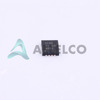
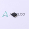
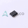
Compact 8-pin WFDFN package
Key Technical Parameters
Gain Bandwidth Product: 20 MHz
Voltage Supply Span (Min/Max): 1.8 V / 5.5 V
Current Supply: 1.45 mA
Slew Rate: 10 V/μs
Voltage Input Offset: 40 μV
Amplifier Type: CMOS
Current Output / Channel: 65 mA
Current Input Bias: 0.2 pA
Operating Temperature: -40°C to 125°C
Quality and Safety Features
RoHS3 compliant
Housed in an 8-pin WFDFN exposed pad package
Compatibility
Designed for surface mount applications
Application Areas
Precision instrumentation and control systems
Sensor signal conditioning
Data acquisition systems
Medical electronics
Industrial automation and control
Product Lifecycle
Active product
Replacement and upgrade options available
Key Reasons to Choose This Product
Excellent precision and stability with low input offset voltage and bias current
Wide operating voltage range and high slew rate for versatile applications
Low power consumption for energy-efficient designs
Compact 8-pin package with exposed pad for improved thermal performance
Broad operating temperature range for use in diverse environmental conditions
RoHS3 compliance for environmental responsibility


 OPA2322AIDRTexas InstrumentsIC CMOS 2 CIRCUIT 8SOIC
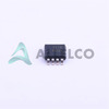 OPA2322AIDGKTTexas InstrumentsIC CMOS 2 CIRCUIT 8VSSOP
 OPA2322AIDTexas InstrumentsIC CMOS 2 CIRCUIT 8SOIC
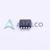 OPA2320AQDGKRQ1Texas InstrumentsIC CMOS 2 CIRCUIT 8VSSOP
 OPA2322AIDGKRTexas InstrumentsIC CMOS 2 CIRCUIT 8VSSOP
 OPA2320AIDGKRTexas InstrumentsIC CMOS 2 CIRCUIT 8VSSOP
 OPA2320AQDGKRQ1TWTexas Instruments


