
Manufacturer Part Number
TPS43335QDAPRQ1
Manufacturer
Texas Instruments
Introduction
The TPS43335QDAPRQ1 is a versatile DC DC Switching Controller designed for power management applications. It is suitable for automotive environments and offers flexibility in creating step-up or step-down voltage configurations.
Product Features and Performance
Functions include Step-Up and Step-Down voltage conversion
Supports both Buck and Boost topologies
Features three outputs and two output phases
Supply voltage range from 4V to 40V
Operates at switching frequencies between 150kHz to 600kHz
Supports up to 98.75% duty cycle for efficient power management
Integrated synchronous rectifier for reduced power dissipation
Clock synchronization capability
Control features: Enable, Frequency Control, Power Good, Soft Start, Tracking
Product Advantages
High flexibility in voltage management
Automatic synchronization for system integration
Robust control features enable precise power management
Suitable for harsh automotive environments
Key Technical Parameters
Voltage Supply (Vcc/Vdd): 4V ~ 40V
Switching Frequency: 150kHz ~ 600kHz
Maximum Duty Cycle: 90%, 98.75%
Operating Temperature: -40°C ~ 125°C (TJ)
Quality and Safety Features
Operates reliably in a broad temperature range (-40°C to 125°C)
AEC-Q100 qualified for automotive applications
Compatibility
Compatible with a wide range of input voltages (4V to 40V)
Seamlessly integrates with automotive voltage systems
Application Areas
Automotive electronic systems
Power management modules
Renewable energy systems
Product Lifecycle
Currently active product status
No indication of nearing discontinuation, ensuring long-term availability
Several Key Reasons to Choose This Product
Flexibility in creating various voltage configurations (step-up or step-down)
Supports precise power control and management in automotive systems
High-efficiency design with synchronous rectification and adjustable switching frequency
Durable and reliable under extreme automotive conditions
Proven safety with AEC-Q100 qualification


 TPS43332EVMTexas InstrumentsEVAL MODULE FOR TPS43332
 TPS43330EVMTexas InstrumentsEVAL MODULE FOR TPS43330
 TPS43331EVMTexas InstrumentsEVAL MODULE FOR TPS43331
 TPS43336EVMTexas InstrumentsEVAL MODULE FOR TPS43336
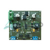 TPS43351EVMTexas InstrumentsEVAL MODULE FOR TPS43351
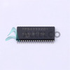 TPS43332QDAPRQ1Texas InstrumentsIC REG CTRLR BUCK/BOOST 38HTSSOP
 TPS43340EVMTexas InstrumentsEVAL MODULE FOR TPS43340
 TPS43335EVMTexas InstrumentsEVAL MODULE FOR TPS43335
 TPS43350EVMTexas InstrumentsEVAL MODULE FOR TPS43350


