
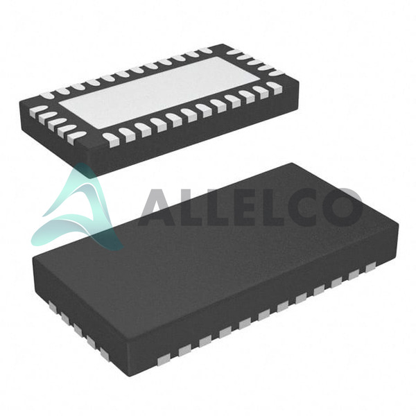
TPS54917RUVT (1)
Manufacturer Part Number
TPS54917RUVT
Manufacturer
Texas Instruments
Introduction
High-performance, synchronous, step-down DC/DC converter
Optimized for high-current, high-efficiency power conversion
Product Features and Performance
Wide input voltage range: 3V to 4V
Adjustable output voltage from 0.891V to 3.6V
Up to 9A output current capability
High efficiency: up to 95%
Switching frequency options: 350kHz and 550kHz
Integrated power MOSFETs
Protection features: overcurrent, overvoltage, undervoltage, thermal shutdown
Product Advantages
Compact design with high power density
Excellent transient response and load regulation
Flexible configuration options
Robust protection features for reliable operation
Key Technical Parameters
Input voltage range: 3V to 4V
Output voltage range: 0.891V to 3.6V
Output current: up to 9A
Switching frequency: 350kHz or 550kHz
Operating temperature range: -40°C to 125°C
Quality and Safety Features
RoHS3 compliant
Robust thermal management design
Overcurrent, overvoltage, and undervoltage protection
Compatibility
Suitable for a wide range of applications that require high-efficiency, high-current power conversion
Application Areas
Portable electronics
Industrial equipment
Networking and telecommunication equipment
Automotive electronics
Product Lifecycle
Currently in production
Replacement or upgrade options available from Texas Instruments
Key Reasons to Choose This Product
High-efficiency power conversion with up to 95% efficiency
Flexible configuration options to match various application requirements
Robust protection features for reliable operation
Compact design with high power density
Excellent transient response and load regulation
Wide operating temperature range of -40°C to 125°C


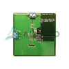 TPS54917EVM-367Texas InstrumentsEVAL MODULE FOR TPS54917-367
 TPS54900PWRTexas InstrumentsIC REG BCK PROG 100MA QD 16TSSOP
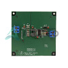 TPS54972EVM-222Texas InstrumentsEVAL MOD FOR TPS54972
 TPS54973EVM-017Texas InstrumentsEVAL MODULE FOR TPS54973-017


