
Manufacturer Part Number
LM2735YSD/NOPB
Manufacturer
Texas Instruments
Introduction
The LM2735YSD/NOPB is a high-efficiency, step-up/step-down DC-DC converter capable of providing up to 2.1A of output current. It features an adjustable output voltage range from 3V to 24V, making it suitable for a wide variety of applications.
Product Features and Performance
High efficiency of up to 95%
Wide input voltage range of 2.7V to 5.5V
Adjustable output voltage from 3V to 24V
Maximum output current of 2.1A
Switching frequency of 520kHz
Thermal shutdown and overcurrent protection
Small 6-WDFN package with exposed thermal pad
Product Advantages
Versatile step-up/step-down operation for flexible power supply designs
High efficiency for improved energy savings and thermal management
Wide output voltage range accommodates various system requirements
Compact package size for space-constrained applications
Key Reasons to Choose This Product
Excellent power conversion efficiency for enhanced system performance
Flexible output voltage configuration to match diverse application needs
Robust protection features for reliable and safe operation
Small form factor enables compact power supply designs
Quality and Safety Features
Thermal shutdown protection
Overcurrent protection
RoHS-compliant and lead-free package
Compatibility
The LM2735YSD/NOPB is compatible with a wide range of electronic devices and systems that require a flexible and efficient power supply solution.
Application Areas
Portable electronics
Industrial equipment
Automotive applications
Medical devices
Telecommunications equipment
Product Lifecycle
The LM2735YSD/NOPB is an active product, and there are no plans for discontinuation at this time. Texas Instruments offers several equivalent and alternative models, such as the LM2735-Q1, LM2735-ADJ, and LM2735-ADJ/NOPB, which may be suitable depending on specific application requirements. For more information, please contact our website's sales team.
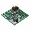 LM2735YSDEVALTexas InstrumentsBOARD EVAL LM2735 520KHZ 6LLP
 LM2735YMYX/NOPBTexas InstrumentsIC REG MULT CONFG ADJ 2.1A 8MSOP
 LM2736XMK-NSNational SemiconductorSWITCHING REG, CURRENT-MODE, 2.3
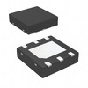 LM2735YQSD/NOPBTexas InstrumentsIC REG MULT CONFG ADJ 2.1A 6WSON
 LM2736XMKTexas InstrumentsIC REG BUCK ADJ 750MA TSOT23-6
 LM2736XMKXTexas InstrumentsIC REG BUCK ADJ 750MA TSOT23-6
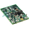 LM2736X EVAL/NOPBTexas InstrumentsEVAL BOARD FOR LM2736X
 LM2735YQMFX/NOPBTexas InstrumentsIC REG MULT CONFG ADJ 2.1A SOT23
 LM2736XMK/NOPBTexas Instruments
 LM2735YSDNS


