View All

Please refer to the English Version as our Official Version.Return

Europe
France(Français) Germany(Deutsch) Italy(Italia) Russian(русский) Poland(polski) Czech(Čeština) Luxembourg(Lëtzebuergesch) Netherlands(Nederland) Iceland(íslenska) Hungarian(Magyarország) Spain(español) Portugal(Português) Turkey(Türk dili) Bulgaria(Български език) Ukraine(Україна) Greece(Ελλάδα) Israel(עִבְרִית) Sweden(Svenska) Finland(Svenska) Finland(Suomi) Romania(românesc) Moldova(românesc) Slovakia(Slovenská) Denmark(Dansk) Slovenia(Slovenija) Slovenia(Hrvatska) Croatia(Hrvatska) Serbia(Hrvatska) Montenegro(Hrvatska) Bosnia and Herzegovina(Hrvatska) Lithuania(lietuvių) Spain(Português) Switzerland(Deutsch) United Kingdom(English)
Asia/Pacific
Japan(日本語) Korea(한국의) Thailand(ภาษาไทย) Malaysia(Melayu) Singapore(Melayu) Vietnam(Tiếng Việt) Philippines(Pilipino)
Africa, India and Middle East
United Arab Emirates(العربية) Iran(فارسی) Tajikistan(فارسی) India(हिंदी) Madagascar(malaɡasʲ)
South America / Oceania
New Zealand(Maori) Brazil(Português) Angola(Português) Mozambique(Português)
North America
United States(English) Canada(English) Haiti(Ayiti) Mexico(español)
HomeProductsIntegrated Circuits (ICs)Specialized ICsUC1825AJ
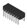
Image may be representation.
See specifications for product details.
EXPRESS OPTION
Payment method

UC1825AJ - Texas Instruments

Manufacturer Part Number
UC1825AJ
Manufacturer
Texas Instruments
Allelco Part Number
32D-UC1825AJ
Warranty
1 Year Allelco Warranty - Find out more
Stock Status:
15,380 pcs available, New & Original
Parts Description
DAC91001
Data sheet
-
Category
Integrated Circuits (ICs) > Specialized ICs
RoHs Status
Our certification
In stock: 15380

Required fields are indicated by an asterisk (*)
Please send RFQ, we will respond immediately.

Quantity

Specifications

UC1825AJ Tech Specifications
Texas Instruments - UC1825AJ technical specifications, attributes, parameters and parts with similar specifications to Texas Instruments - UC1825AJ

Product Attribute Attribute Value
Part Number UC1825AJ
Package DAC91001
Description DAC91001
Stock Condition Get 15380 pcs available quantity at Allelco
Payment PayPal / TT / Credit Card / Western Union
Allelco Certifications ESD / ISO 9001 / ISO 13485 / ISO 28000
Product Attribute Attribute Value
Manufacturer Texas Instruments
RoHs Status -
Warranty 100% Perfect Functions
Transport port Hong Kong
Shipping by DHL / FedEx / UPS / TNT / SF Express
RFQ Email info@allelco.com

Parts Introduction

Manufacturer Part Number

UC1825AJ

Manufacturer

Texas Instruments

Introduction

The UC1825AJ is a versatile power management (PMIC) DC-DC switching controller that offers a range of features and functionalities. It is designed to provide efficient and reliable power conversion solutions for various applications.

Product Features and Performance

Supports step-up, step-down, and step-up/step-down power conversion

Offers multiple topologies, including boost, buck, flyback, forward converter, full-bridge, half-bridge, and push-pull

Provides two output phases for improved efficiency and reduced output ripple

Operates at a switching frequency range of 400kHz to 1MHz

Supports a maximum duty cycle of 50%

Includes synchronous rectifier and clock sync features

Offers control features like dead time control and soft start

Product Advantages

Efficient power conversion with multiple topology options

Improved performance and reduced output ripple with dual-phase operation

Wide operating frequency range for design flexibility

Robust control features for enhanced system performance

Key Reasons to Choose This Product

Versatile power conversion capabilities to meet diverse application requirements

Optimized efficiency and reduced output ripple for improved system performance

Reliable and robust design for long-term operation

Comprehensive control features for enhanced system control and protection

Quality and Safety Features

Wide operating temperature range of -55°C to 125°C (TA)

Through-hole mounting for robust and secure installation

16-CDIP (0.300", 7.62mm) package for reliable and space-efficient integration

Compatibility

The UC1825AJ is a general-purpose power management (PMIC) DC-DC switching controller that can be used in a wide range of applications.

Application Areas

Industrial automation and control systems

Telecommunications and networking equipment

Automotive electronics

Medical devices

Renewable energy systems

General power conversion applications

Product Lifecycle

The UC1825AJ is an active product, and our website's sales team continues to offer support and availability for this model. There are no immediate plans for discontinuation or replacement. However, as technology evolves, customers are advised to consult with our website's sales team for the latest information on product availability and any potential equivalent or alternative models that may be introduced in the future.
Frequently Asked Questions(FAQ)

What are the key performance trade-offs when using the UC1825AJ in a dual-phase buck converter configuration for high-efficiency power delivery systems?
The UC1825AJ supports two independent output phases, enabling interleaved switching that reduces input and output ripple current. However, each phase is limited to a 50% maximum duty cycle, which restricts voltage step-up capability in boost applications. When configured as a dual-buck controller, this constraint means the output voltage cannot significantly exceed the input voltage by more than a small margin. Additionally, while the 400kHz to 1MHz switching frequency range allows compact magnetics, higher frequencies increase gate drive losses and electromagnetic interference. Designers must balance efficiency, thermal performance, and PCB layout complexity against these inherent limitations.
How does the UC1825AJ compare to the UC1823A in terms of topology flexibility and control architecture when selecting a controller for a forward converter design?
The UC1825AJ offers broader topology support, including full-bridge, half-bridge, and push-pull configurations, whereas the UC1823A is optimized primarily for single-ended forward and flyback topologies. Both share similar supply voltage ranges (12V–20V) and dead time control, but the UC1825AJ includes an integrated soft-start feature and supports dual-output phases, making it more suitable for distributed power architectures requiring multiple isolated outputs. The UC1823A, however, may offer lower quiescent current in simpler, single-switch applications. For forward converters with tight transient response requirements, the UC1825AJ’s advanced control features provide better dynamic regulation under load steps.
What are the implications of operating the UC1825AJ at the upper end of its switching frequency range (near 1 MHz) in a high-power flyback application?
Operating near 1 MHz increases switching losses due to higher gate charge dissipation and core losses in the transformer. While this enables smaller passive components and reduced board area, it also raises junction temperature, especially in continuous conduction mode (CCM) flybacks above 200 W. The UC1825AJ’s internal oscillator and gate drivers are rated for this range, but efficiency typically drops by 3% to 5% compared to operation at 400 kHz. Thermal management becomes critical, and snubber circuits may be required to mitigate ringing. This trade-off favors space-constrained designs where size outweighs moderate efficiency penalties.
Can the UC1825AJ be used in a synchronous rectification topology, and what are the limitations if attempting to implement it externally?
The UC1825AJ does not include integrated synchronous rectifier (SR) drivers; it provides standard transistor driver outputs for external MOSFETs. While it can be used in conjunction with discrete SR control logic or external controllers for synchronous operation, doing so adds complexity and cost. The lack of built-in dead time sensing for both high-side and low-side transitions requires careful external timing design to avoid shoot-through. In practice, many designers use the UC1825AJ for asynchronous conversion and pair it with dedicated SR FET drivers only when efficiency gains justify the added circuitry.
What design considerations are essential when interfacing the UC1825AJ with optocouplers in an isolated forward converter to ensure stable feedback loop operation?
Stable feedback requires minimizing propagation delay mismatch between the optocoupler and the UC1825AJ’s error amplifier. The device’s internal soft-start and dead time control help prevent overshoot during startup, but phase margin degradation due to optoisolator delay can reduce stability margins below 45° in wide-input designs. Compensation networks must account for the total loop delay, typically limiting bandwidth to below 10 kHz in galvanically isolated systems. Additionally, common-mode transient immunity (CMTI) of the optocoupler must exceed 50 kV/µs to maintain reliable operation across industrial environments. Proper placement of the compensation capacitor and use of low-offset amplifiers further enhance phase margin.
How does the UC1825AJ handle load transient response in a multi-phase boost configuration, and what external components influence this behavior?
In a dual-phase boost setup, the UC1825AJ achieves improved transient response through interleaving, reducing peak di/dt on the input filter. However, each phase operates independently, so rapid load steps still induce ripple proportional to the inductor values and switching frequency. The output capacitance must be sized to absorb energy during the controller’s response time, which is governed by the error amplifier bandwidth (typically < 50 kHz). Increasing output capacitance improves hold-up but slows response; conversely, smaller capacitors risk voltage droop. A well-designed system uses low-ESR ceramics with bulk electrolytic or polymer capacitors to balance stability and transient performance.
Is it feasible to use the UC1825AJ for battery-powered applications requiring wide duty cycle adjustment beyond 50%, and what modifications would be needed?
No, the UC1825AJ has a fixed 50% maximum duty cycle, making it unsuitable for pure boost modes requiring >50% duty cycle without additional circuitry. To extend boost capability, a pre-boost stage or a secondary controller like the UC1823A could precede the UC1825AJ. Alternatively, a buck-boost topology must be implemented using external switches and diodes, bypassing the IC’s internal structure. This approach sacrifices simplicity and increases component count. For most battery-powered systems where boost ratios remain modest (e.g., 1.2:1), the 50% limit is acceptable, but higher ratios require alternative architectures.
What precautions should be taken when mounting the UC1825AJ in a high-temperature industrial environment exceeding 100°C ambient?
The UC1825AJ is specified for operation up to 125°C, but derating is necessary near the upper limit. Gate drive strength decreases slightly at elevated temperatures, potentially increasing turn-on resistance and conduction losses in high-current applications. Thermal vias under the CDIP package must be properly connected to a solid ground plane to dissipate heat efficiently. In designs exceeding 100°C ambient, airflow or heatsinking may be required, even though the package lacks exposed pads. Monitoring junction temperature through external sensors or empirical testing ensures reliability, as long-term exposure near 125°C accelerates electromigration in bond wires.
How does the UC1825AJ support clock synchronization in multi-controller systems, and what challenges arise when syncing multiple units?
The UC1825AJ includes a clock synchronization input that allows external clock signals to override its internal oscillator, ensuring all controllers operate at the same frequency—critical for EMI reduction and harmonic avoidance. When synchronizing multiple UC1825AJ devices, skew between clock inputs can cause phase misalignment, reducing interleaving benefits. Tight PCB trace matching (<5 mm difference in length) and use of differential pairs minimize skew. Additionally, the master clock source must have low jitter (<1 ns RMS) to prevent subharmonic oscillation or instability. Failure to match timing precisely degrades ripple cancellation and increases input stress.
What role does dead time control play in the UC1825AJ when driving complementary MOSFETs in a half-bridge topology?
Dead time control prevents simultaneous conduction of high-side and low-side switches, avoiding shoot-through current and protecting the MOSFETs from excessive power loss. The UC1825AJ integrates adjustable dead time into its driver outputs, allowing precise spacing between turn-off and turn-on transitions. Insufficient dead time risks cross-conduction and thermal failure; excessive dead time causes body diode conduction, increasing losses in ZVS-capable designs. Optimal dead time depends on MOSFET gate capacitance, drive strength, and switching speed—typically set between 100 ns and 500 ns. External RC networks or dedicated driver ICs can refine this timing for best efficiency.
Can the UC1825AJ be safely operated with a supply voltage below 12 V, and what are the consequences of undervoltage conditions?
No, the UC1825AJ requires a minimum supply voltage of 12 V (Vcc/Vdd). Operating below this threshold disables proper internal biasing, leading to erratic switching behavior, incomplete soft-start sequences, or failure to initiate oscillation. If the system voltage occasionally dips below 12 V (e.g., during brownouts), an auxiliary bias regulator or bulk capacitor may maintain Vcc above threshold momentarily. However, sustained undervoltage results in unstable output and potential damage due to partial conduction states. Always ensure input filtering and sufficient decoupling capacitance to keep Vcc within specification under worst-case transients.
How do the two independent output channels of the UC1825AJ interact when sharing a common load, and what layout considerations prevent crosstalk?
The two outputs can be paralleled for higher current delivery or run independently for dual-voltage rails. When paralleled, magnetic coupling between inductors can induce noise if not spatially separated. Interleaved operation reduces ripple but demands careful PCB routing: return paths must be minimized, and ground planes kept solid beneath switching nodes. High-current traces should avoid crossing under sensitive analog sections. Decoupling capacitors must be placed close to each channel’s input pin to suppress inter-phase coupling. Poor layout leads to audible noise, reduced efficiency, or unstable regulation due to mutual inductance effects.
What is the significance of the 16-CDIP package in terms of thermal performance and mechanical robustness for industrial applications?
The 16-lead ceramic dual in-line package (CDIP) offers superior thermal conductivity compared to plastic DIP alternatives, enabling better heat dissipation in high-power designs. Its ceramic construction resists moisture ingress and withstands thermal cycling, making it ideal for harsh environments. However, it is heavier and more fragile than plastic packages, requiring careful handling during assembly. Mounting directly onto a metal chassis can further improve thermal resistance (θJA), but mechanical stress must be managed to avoid cracking. For applications with high ambient temperatures or continuous full-load operation, the CDIP’s thermal advantages make the UC1825AJ a reliable choice despite its size.
Does the UC1825AJ support fault detection features such as overcurrent or thermal shutdown, and how do these protect downstream components?
The UC1825AJ does not include integrated overcurrent protection or overtemperature shutdown; it relies on external circuitry for fault mitigation. Designers typically implement current sensing via shunt resistors or Hall-effect sensors feeding into comparators that disable the enable pin during overloads. Without such safeguards, shorted loads or excessive MOSFET currents can destroy the IC or passives. Soft-start helps limit inrush during startup, but sustained overvoltage or overcurrent events require external protection. This design philosophy places responsibility on the system-level designer, offering flexibility but demanding rigorous safety analysis.
How does the operating temperature range (-55°C to 125°C) affect long-term reliability in automotive or aerospace applications using the UC1825AJ?
The wide temperature range meets military and automotive standards (e.g., AEC-Q100 Grade 1), indicating robust construction. At -55°C, semiconductor mobility decreases slightly, increasing propagation delay but improving latch-up immunity. At 125°C, electromigration in aluminum interconnects accelerates, so current density must be limited in layout. Solder joint fatigue becomes a concern under thermal cycling, necessitating conformal coating or strain relief. While the IC itself is qualified, peripheral components (capacitors, MOSFETs) must also meet extended temperature specs. System-level derating—operating below 100°C at full load—extends mean time between failures (MTBF).
What are the advantages of using the UC1825AJ in a full-bridge converter compared to a half-bridge, particularly regarding voltage stress and transformer utilization?
In a full-bridge converter driven by the UC1825AJ, the transformer primary sees only half the DC bus voltage, reducing insulation stress and enabling higher efficiency in high-power (>1 kW) applications. The UC1825AJ’s dual outputs allow simultaneous excitation of both windings, achieving higher power transfer and better transformer utilization (up to 50%) compared to half-bridge (≈25%). However, full-bridge requires four MOSFETs and more complex gate driving, increasing cost and layout complexity. The UC1825AJ’s dead time control ensures safe commutation, but timing precision becomes critical to avoid voltage overshoots. Overall, the full-bridge topology suits medium-to-high-power isolated supplies where efficiency and reliability outweigh component count.

Customer Reviews

Evaluation: 10 Articles

  • ECUb***h
    Sep 22, 2026

    Used for repair of an older automotive ECU. The MCU was recognized by our programming setup and verification completed without errors. The repaired board now starts and communicates normally.

  • RS48***ieldTech
    Sep 16, 2026

    Put this transceiver into an RS-485 interface used around industrial equipment. Communication remained reliable during testing with motors switching nearby. Good result for the replacement board.

  • Logi***b_Chris
    Sep 8, 2026

    Purchased for a Cyclone III development project. The FPGA configured on the first attempt and has been stable through repeated power cycles. No problems with the I/O we are using.

  • Circ***FixerTom
    Sep 2, 2026

    Used this rectifier in a high-current power supply repair. Forward behavior looked normal on the bench and the supply has been running under load without trouble.

  • Retr***UWorks
    Aug 31, 2026

    Needed the exact ST10F269Z2Q6 for servicing an older control unit. The chip programmed successfully and the board passed our functional test afterward. Much easier than redesigning around a newer MCU.

  • Andr***PCBLab
    Aug 28, 2026

    I needed this ADC for an older data acquisition board. Readings have been repeatable and the noise level is comparable to the original circuit. Happy with the purchase.

  • Leat***O'Keefe
    Aug 20, 2026

    one of my hobbies is skydiving. and when i'm skydiving this works great.

  • Ilen***
    Aug 20, 2026

    This product works considerably well. It secretly improves my basketball by a lot.

  • Indu***ialPower
    Aug 17, 2026

    Installed this IGBT module in a power conversion cabinet. Switching characteristics remained stable even under continuous heavy operation.

  • Nikh***ech
    Aug 13, 2026

    Great low-power MCU for portable equipment. Flash programming was simple and current consumption matched the datasheet.

Write a Review

Your Email address will not be published.

Shipment

Delivery Time

In-stock items can be shipped within 24 hours. Some parts will be arranged for delivery within 1-2 days from the date all items arrive at our warehouse. And Allelco ships order once a day at about 17:00, except Sunday. Once the goods are shipped, the estimated delivery time depends on the shipping methods and Delivery destination. The table below shows are the logistic time for some common countries.

Delivery Cost

  1. Use your express account for shipment if you have one.
  2. Use our account for the shipment. Refer to the table below for the approximate charges.
(Different time frame / countries / package size has different price.)

Delivery Method

  1. Global Common Shipment by DHL / UPS / FedEx / TNT / EMS / SF we support.
  2. Others more shipping ways, please get in touch with your customer manager.

Common Countries Logistic Time Reference
Region Country Logistic Time(Day)
America United States 5
Brazil 7
Europe Germany 5
United Kingdom 4
Italy 5
Oceania Australia 6
New Zealand 5
Asia India 4
Japan 4
Middle East Israel 6
DHL & FedEx Shipment Charges Reference
Shipment charges(KG) Reference DHL(USD$)
0.00kg-1.00kg USD$30.00 - USD$60.00
1.00kg-2.00kg USD$40.00 - USD$80.00
2.00kg-3.00kg USD$50.00 - USD$100.00
Note:
The above table is for reference only. There may have some data bias for the uncontrollable factors.
Contact us if you have any questions.
  • QC (Quality Warranty)
  • Payment Support
  • Packaging
  • Certifications & Memberships

QC (Quality Warranty)

Allelco is committed to exceeding customer expectations through customer service excellence, order accuracy, and on-time delivery.
This is achieved through our commitment to the continual improvement of our processes, services, and products.


Strict quality inspection builds a solid foundation for electronic component quality.
  1. Visual inspection
  2. Performance testing and reliability verification
  3. Standardized full-process testing
  4. Precise control of every parameter
We eliminate defective components and ensure the stable operation of electronic devices through professional quality standards.

Payment Support

The payment method can be chosen from the methods shown below: Wire Transfer (T/T, Bank Transfer), Western Union, Credit card, PayPal.
  • HKBea
  • Paypal
  • MasterCard
  • Western-Union
  • VISA
Stable Delivery, Sincere Partnership — Your Faithful Supply Chain Partner
  • Efficient Supply Management
  • Cost-Saving Procurement
  • Fast Sourcing & Delivery
Contact us if you have any questions.

Packaging

Electrostatic Discharge Protection and Handling

All electrostatic-sensitive components are handled in accordance with electrostatic discharge control procedures. The products are hermetically sealed in anti-static safe packaging to prevent electrostatic damage. Appropriate labeling is also applied for identification and traceability. This ensures product integrity during storage, handling and transportation.


ESD

Certifications & Memberships

Third-party certified, strict quality control. Our certification
  • ISO 9001: 2015
  • ISO 13485: 2016
  • ISO 14001: 2015
  • ISO 28000: 2007
  • ISO 45001: 2018
  • GB/T 27922-2011
  • SMTA
  • IPC
  • ESD
  • PSMA
Texas Instruments

UC1825AJ

Texas Instruments
32D-UC1825AJ

Want a better price? Add to Cart and Submit RFQ now, we'll contact you immediately.

0 RFQ
Shopping cart (0 Items)
It is empty.
Compare List (0 Items)
It is empty.
Feedback

Your feedback matters! At Allelco, we value the user experience and strive to improve it constantly.
Please share your comments with us via our feedback form, and we'll respond promptly.
Thank you for choosing Allelco.

Subject
E-mail
Comments
Captcha
Drag or click to upload file
Upload File
types: .xls, .xlsx, .doc, .docx, .jpg, .png and .pdf.
Max file size: 10MB












