View All

Please refer to the English Version as our Official Version.Return

Europe
France(Français) Germany(Deutsch) Italy(Italia) Russian(русский) Poland(polski) Czech(Čeština) Luxembourg(Lëtzebuergesch) Netherlands(Nederland) Iceland(íslenska) Hungarian(Magyarország) Spain(español) Portugal(Português) Turkey(Türk dili) Bulgaria(Български език) Ukraine(Україна) Greece(Ελλάδα) Israel(עִבְרִית) Sweden(Svenska) Finland(Svenska) Finland(Suomi) Romania(românesc) Moldova(românesc) Slovakia(Slovenská) Denmark(Dansk) Slovenia(Slovenija) Slovenia(Hrvatska) Croatia(Hrvatska) Serbia(Hrvatska) Montenegro(Hrvatska) Bosnia and Herzegovina(Hrvatska) Lithuania(lietuvių) Spain(Português) Switzerland(Deutsch) United Kingdom(English)
Asia/Pacific
Japan(日本語) Korea(한국의) Thailand(ภาษาไทย) Malaysia(Melayu) Singapore(Melayu) Vietnam(Tiếng Việt) Philippines(Pilipino)
Africa, India and Middle East
United Arab Emirates(العربية) Iran(فارسی) Tajikistan(فارسی) India(हिंदी) Madagascar(malaɡasʲ)
South America / Oceania
New Zealand(Maori) Brazil(Português) Angola(Português) Mozambique(Português)
North America
United States(English) Canada(English) Haiti(Ayiti) Mexico(español)
HomeProductsIntegrated Circuits (ICs)Embedded - FPGAs (Field Programmable Gate Array)M2GL010-VF400
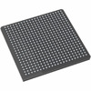
M2GL010-VF400 Image
Image may be representation.
See specifications for product details.
EXPRESS OPTION
Payment method

M2GL010-VF400 - Microchip Technology

Manufacturer Part Number
M2GL010-VF400
Manufacturer
Microchip Technology
Allelco Part Number
98D-M2GL010-VF400
Warranty
1 Year Allelco Warranty - Find out more
Stock Status:
29,094 pcs available, New & Original
Parts Description
IC FPGA 195 I/O 400VFBGA
Package
400-VFBGA (17x17)
Data sheet
M2GL010-VF400.pdf
RoHs Status
 
Our certification
In stock: 29094
  • Unit Price: $36.35
  • Subtotal: $0.00

Want a better price?
Add to Cart and Submit RFQ now, we'll contact you immediately.

Quantity Unit Price Ext. Price
1+ $36.35 $36.35
200+ $14.07 $2,814.00
500+ $13.57 $6,785.00
1000+ $13.33 $13,330.00
The above prices does not include taxes and freight rates, which will be calculated on the order pages.


Specifications

M2GL010-VF400 Tech Specifications
Microchip Technology - M2GL010-VF400 technical specifications, attributes, parameters and parts with similar specifications to Microchip Technology - M2GL010-VF400

Product Attribute Attribute Value
Manufacturer Microchip Technology
Voltage - Supply 1.14V ~ 2.625V
Total RAM Bits 933888
Supplier Device Package 400-VFBGA (17x17)
Series IGLOO2
Package / Case 400-LFBGA
Product Attribute Attribute Value
Package Tray
Operating Temperature 0°C ~ 85°C (TJ)
Number of Logic Elements/Cells 12084
Number of I/O 195
Mounting Type Surface Mount
Base Product Number M2GL010

Environmental & Export Classifications

ATTRIBUTE DESCRIPTION
RoHs Status RoHS non-compliant
Moisture Sensitivity Level (MSL) 3 (168 Hours)
REACH Status REACH Unaffected
ECCN 3A991D
HTSUS 8542.39.0001

Frequently Asked Questions(FAQ)

What are the key power and thermal considerations when integrating the M2GL010-VF400 into a high-reliability embedded system operating at elevated ambient temperatures?
The M2GL010-VF400 operates across a supply voltage range of 1.14V to 2.625V, with typical dynamic current consumption scaling quadratically with frequency and voltage. At 1.2V core supply and moderate switching activity, dynamic power can reach several hundred milliwatts per square millimeter of logic area. Given its 12084 logic elements and 933888-bit RAM, peak instantaneous power may exceed 2W under worst-case conditions. Coupled with a maximum junction temperature of 85°C, thermal resistance from junction to ambient must be carefully evaluated in compact enclosures. Designers should allocate sufficient PCB copper area for heat spreading, consider airflow, and verify that steady-state junction temperature remains below 70°C even during sustained load. Failure to manage thermal dissipation may lead to functional throttling or accelerated aging due to the non-compliant RoHS status, which also limits solder options in sensitive environments.
How does the pin count and package configuration of the M2GL010-VF400 influence board layout complexity and signal integrity requirements compared to larger IGLOO2 devices like the M2GL050?
The M2GL010-VF400 features 195 I/Os distributed across a 400-ball VFBGA package in a 17x17 mm footprint. This relatively modest I/O count reduces routing congestion but demands precise BGA fanout planning due to small ball pitch (typically 0.8 mm). In contrast, larger IGLOO2 variants such as the M2GL050 offer over 300 I/Os, increasing routing density and requiring more aggressive layer counts or via-in-pad strategies. While the M2GL010’s lower pin count simplifies timing closure and crosstalk mitigation, it still requires controlled impedance routing for high-speed interfaces like LVDS or DDR memory clocks. The shared 400-VFBGA footprint allows mechanical compatibility between M2GL010 and higher-density models, enabling scalable designs where future performance upgrades require minimal mechanical rework—provided power delivery and thermal margins accommodate increased current draw.
What architectural trade-offs arise when choosing the M2GL010-VF400 over ASIC alternatives in low-to-medium volume production runs?
The M2GL010-VF400 offers FPGA programmability and rapid prototyping advantages, eliminating mask costs and enabling design iterations without hardware changes. However, its power efficiency lags behind custom ASIC implementations by approximately 3–5× for comparable functions due to programmable interconnect overhead. For applications requiring fewer than 50k equivalent gates and infrequent updates, an ASIC would deliver superior energy per operation and smaller form factor. Yet, the M2GL010 supports complex state machines, soft processors (e.g., Cortex-M0), and mixed-signal integration within a single die, reducing external component count. In systems where time-to-market outweighs long-term power budget concerns, or where firmware-defined functionality must evolve post-deployment, the M2GL010’s flexibility justifies its higher static and dynamic power consumption relative to purpose-built silicon.
How should designers validate timing closure and I/O bank constraints when deploying the M2GL010-VF400 in a multi-clock domain environment with mixed-voltage peripherals?
The IGLOO2 architecture partitions I/Os into multiple banks, each tied to specific supply rails (typically 1.2V, 1.8V, or 2.5V). The M2GL010-VF400 supports up to three independent I/O voltage domains, but adjacent banks often share decoupling and reference planes. When interfacing 3.3V legacy sensors or 1.8V DDR interfaces, level-shifting circuitry or internal Schmitt triggers must be employed within constrained I/O groups. Timing analysis should account for clock skew between domains and use Microchip’s Libero SoC tools to enforce setup/hold margins under worst-case process-voltage-temperature (PVT) corners. Critical paths crossing clock domains must include explicit synchronization primitives, and asynchronous inputs should be sampled using dual-stage flip-flops to prevent metastability—especially important given the device’s industrial-grade but limited temperature range (0°C to 85°C).
What impact does the Moisture Sensitivity Level 3 (MSL3) rating have on storage, handling, and reflow soldering procedures for the M2GL010-VF400 in mass production?
With an MSL3 classification, the M2GL010-VF400 must be stored in dry packaging (humidity <10%) and baked if exposed to ambient conditions for over 168 hours prior to assembly. During reflow, the cumulative thermal exposure must not exceed the JEDEC J-STD-020 profile’s total time above liquidus (typically <6 seconds above 240°C). Failure to adhere to these guidelines risks popcorning during soldering, leading to internal delamination and latent reliability failures. Production lines should implement real-time humidity monitoring and maintain bake schedules aligned with IPC standards. Given the part’s RoHS non-compliance, lead-free processes are prohibited, further complicating compliance with modern environmental directives and potentially affecting solder joint integrity if improper alloys are used.
Can the M2GL010-VF400 directly drive DDR2 or DDR3 memory interfaces without external PHY support, and what are the performance limitations?
No, the M2GL010-VF400 lacks embedded memory controllers or hard I/O transceivers optimized for DDR signaling. While basic point-to-point communication using LVCMOS I/Os is feasible, achieving stable data rates above 166 MHz (DDR3-333) becomes challenging due to limited slew rate control, absence of DQS deskew logic, and poor noise immunity on shared traces. Successful implementations typically cap speeds at 100–133 MHz with careful termination, length matching (<±50 mil), and ground plane stitching. For higher bandwidth needs, external serial interfaces (e.g., SPI Flash) or FPGA-based soft IP with calibrated delays are preferred. Using the M2GL010 as a memory controller introduces significant resource overhead, consuming up to 40% of available LUTs and RAM blocks, which may negate its advantage over simpler microcontrollers.
How do configuration security features compare between the M2GL010-VF400 and newer IGLOO2 Secure variants, particularly regarding anti-tamper and bitstream encryption capabilities?
The standard M2GL010-VF400 supports basic configuration via SPI flash and includes weak CRC protection, but lacks hardware cryptographic engines or secure boot features present in IGLOO2 Secure devices. Without on-chip AES or SHA accelerators, implementing authenticated firmware updates requires external secure elements, increasing bill-of-materials cost and attack surface. In contrast, Secure variants integrate hardened key storage, tamper detection, and encrypted configuration memory, enabling defense against reverse engineering and unauthorized modifications. If intellectual property protection is critical—such as in medical or defense applications—designers should avoid the M2GL010 unless supplemented with additional security layers, accepting the associated latency, power, and complexity trade-offs.
What are the implications of the M2GL010-VF400’s non-RoHS status on global market compliance, especially in EU and California regulations?
As a RoHS non-compliant device, the M2GL010-VF400 cannot be legally sold in the European Union under Directive 2011/65/EU without exemptions, which typically require formal authorization and justification. Similarly, California’s TSCA Section 6(h) restricts certain lead-containing electronics in consumer goods. While industrial and military end-products may qualify for exemptions, commercial consumer devices face significant regulatory hurdles. Designers considering this FPGA should assess whether migration to a RoHS-compliant alternative (e.g., IGLOO2 Secure) introduces unacceptable latency or cost increases. If proceeding with the M2GL010, thorough documentation of exemption eligibility and supply chain traceability becomes mandatory to avoid customs seizures or product recalls.

Parts with Similar Specifications

The three parts on the right have similar specifications to Microchip Technology M2GL010-VF400

Product Attribute M2GL010-VFG400I M2GL010-VF400I M2GL010-VFG400 M2GL010S-1FG484I
Part Number M2GL010-VFG400I M2GL010-VF400I M2GL010-VFG400 M2GL010S-1FG484I
Manufacturer Microchip Technology Microchip Technology Microchip Technology Microsemi Corporation
Total RAM Bits - - - -
Voltage - Supply - - - -
Mounting Type - Surface Mount Through Hole Surface Mount
Series - - - -
Package / Case - 196-LFBGA 16-DIP (0.300', 7.62mm) 64-VFQFN Exposed Pad
Operating Temperature - -40°C ~ 85°C 0°C ~ 70°C -40°C ~ 85°C
Base Product Number - DAC34H84 MAX500 ADS62P42
Package - Tape & Reel (TR) Tube Tape & Reel (TR)
Number of Logic Elements/Cells - - - -
Supplier Device Package - 196-NFBGA (12x12) 16-PDIP 64-VQFN (9x9)
Number of I/O - - - -

M2GL010-VF400 Datasheet PDF

Download M2GL010-VF400 pdf datasheets and Microchip Technology documentation for M2GL010-VF400 - Microchip Technology.

Datasheets
IGLOO2 FPGAs Product Brief.pdf
PCN Assembly/Origin
Manufacturing Change 23/Feb/2021.pdf
PCN Design/Specification
Datasheet Rev 16/Jun/2022.pdf Datasheet 11/Jan/2023.pdf
PCN Other
Libero SoC Timing Change, IO Glitch Notification C.pdf

Customer Reviews

Evaluation: 10 Articles

  • ECUb***h
    Sep 22, 2026

    Used for repair of an older automotive ECU. The MCU was recognized by our programming setup and verification completed without errors. The repaired board now starts and communicates normally.

  • RS48***ieldTech
    Sep 16, 2026

    Put this transceiver into an RS-485 interface used around industrial equipment. Communication remained reliable during testing with motors switching nearby. Good result for the replacement board.

  • Logi***b_Chris
    Sep 8, 2026

    Purchased for a Cyclone III development project. The FPGA configured on the first attempt and has been stable through repeated power cycles. No problems with the I/O we are using.

  • Circ***FixerTom
    Sep 2, 2026

    Used this rectifier in a high-current power supply repair. Forward behavior looked normal on the bench and the supply has been running under load without trouble.

  • Retr***UWorks
    Aug 31, 2026

    Needed the exact ST10F269Z2Q6 for servicing an older control unit. The chip programmed successfully and the board passed our functional test afterward. Much easier than redesigning around a newer MCU.

  • Andr***PCBLab
    Aug 28, 2026

    I needed this ADC for an older data acquisition board. Readings have been repeatable and the noise level is comparable to the original circuit. Happy with the purchase.

  • Leat***O'Keefe
    Aug 20, 2026

    one of my hobbies is skydiving. and when i'm skydiving this works great.

  • Ilen***
    Aug 20, 2026

    This product works considerably well. It secretly improves my basketball by a lot.

  • Indu***ialPower
    Aug 17, 2026

    Installed this IGBT module in a power conversion cabinet. Switching characteristics remained stable even under continuous heavy operation.

  • Nikh***ech
    Aug 13, 2026

    Great low-power MCU for portable equipment. Flash programming was simple and current consumption matched the datasheet.

Write a Review

Your Email address will not be published.

Shipment

Delivery Time

In-stock items can be shipped within 24 hours. Some parts will be arranged for delivery within 1-2 days from the date all items arrive at our warehouse. And Allelco ships order once a day at about 17:00, except Sunday. Once the goods are shipped, the estimated delivery time depends on the shipping methods and Delivery destination. The table below shows are the logistic time for some common countries.

Delivery Cost

  1. Use your express account for shipment if you have one.
  2. Use our account for the shipment. Refer to the table below for the approximate charges.
(Different time frame / countries / package size has different price.)

Delivery Method

  1. Global Common Shipment by DHL / UPS / FedEx / TNT / EMS / SF we support.
  2. Others more shipping ways, please get in touch with your customer manager.

Common Countries Logistic Time Reference
Region Country Logistic Time(Day)
America United States 5
Brazil 7
Europe Germany 5
United Kingdom 4
Italy 5
Oceania Australia 6
New Zealand 5
Asia India 4
Japan 4
Middle East Israel 6
DHL & FedEx Shipment Charges Reference
Shipment charges(KG) Reference DHL(USD$)
0.00kg-1.00kg USD$30.00 - USD$60.00
1.00kg-2.00kg USD$40.00 - USD$80.00
2.00kg-3.00kg USD$50.00 - USD$100.00
Note:
The above table is for reference only. There may have some data bias for the uncontrollable factors.
Contact us if you have any questions.
  • QC (Quality Warranty)
  • Payment Support
  • Packaging
  • Certifications & Memberships

QC (Quality Warranty)

Allelco is committed to exceeding customer expectations through customer service excellence, order accuracy, and on-time delivery.
This is achieved through our commitment to the continual improvement of our processes, services, and products.


Strict quality inspection builds a solid foundation for electronic component quality.
  1. Visual inspection
  2. Performance testing and reliability verification
  3. Standardized full-process testing
  4. Precise control of every parameter
We eliminate defective components and ensure the stable operation of electronic devices through professional quality standards.

Payment Support

The payment method can be chosen from the methods shown below: Wire Transfer (T/T, Bank Transfer), Western Union, Credit card, PayPal.
  • HKBea
  • Paypal
  • MasterCard
  • Western-Union
  • VISA
Stable Delivery, Sincere Partnership — Your Faithful Supply Chain Partner
  • Efficient Supply Management
  • Cost-Saving Procurement
  • Fast Sourcing & Delivery
Contact us if you have any questions.

Packaging

Electrostatic Discharge Protection and Handling

All electrostatic-sensitive components are handled in accordance with electrostatic discharge control procedures. The products are hermetically sealed in anti-static safe packaging to prevent electrostatic damage. Appropriate labeling is also applied for identification and traceability. This ensures product integrity during storage, handling and transportation.


ESD

Certifications & Memberships

Third-party certified, strict quality control. Our certification
  • ISO 9001: 2015
  • ISO 13485: 2016
  • ISO 14001: 2015
  • ISO 28000: 2007
  • ISO 45001: 2018
  • GB/T 27922-2011
  • SMTA
  • IPC
  • ESD
  • PSMA
M2GL010-VF400 Image

M2GL010-VF400

Microchip Technology
98D-M2GL010-VF400

Want a better price? Add to Cart and Submit RFQ now, we'll contact you immediately.

0 RFQ
Shopping cart (0 Items)
It is empty.
Compare List (0 Items)
It is empty.
Feedback

Your feedback matters! At Allelco, we value the user experience and strive to improve it constantly.
Please share your comments with us via our feedback form, and we'll respond promptly.
Thank you for choosing Allelco.

Subject
E-mail
Comments
Captcha
Drag or click to upload file
Upload File
types: .xls, .xlsx, .doc, .docx, .jpg, .png and .pdf.
Max file size: 10MB