View All

Please refer to the English Version as our Official Version.Return

Europe
France(Français) Germany(Deutsch) Italy(Italia) Russian(русский) Poland(polski) Czech(Čeština) Luxembourg(Lëtzebuergesch) Netherlands(Nederland) Iceland(íslenska) Hungarian(Magyarország) Spain(español) Portugal(Português) Turkey(Türk dili) Bulgaria(Български език) Ukraine(Україна) Greece(Ελλάδα) Israel(עִבְרִית) Sweden(Svenska) Finland(Svenska) Finland(Suomi) Romania(românesc) Moldova(românesc) Slovakia(Slovenská) Denmark(Dansk) Slovenia(Slovenija) Slovenia(Hrvatska) Croatia(Hrvatska) Serbia(Hrvatska) Montenegro(Hrvatska) Bosnia and Herzegovina(Hrvatska) Lithuania(lietuvių) Spain(Português) Switzerland(Deutsch) United Kingdom(English)
Asia/Pacific
Japan(日本語) Korea(한국의) Thailand(ภาษาไทย) Malaysia(Melayu) Singapore(Melayu) Vietnam(Tiếng Việt) Philippines(Pilipino)
Africa, India and Middle East
United Arab Emirates(العربية) Iran(فارسی) Tajikistan(فارسی) India(हिंदी) Madagascar(malaɡasʲ)
South America / Oceania
New Zealand(Maori) Brazil(Português) Angola(Português) Mozambique(Português)
North America
United States(English) Canada(English) Haiti(Ayiti) Mexico(español)
HomeProductsIntegrated Circuits (ICs)MemoryPC28F640J3D75B TR
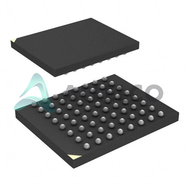
PC28F640J3D75B TR Image
Image may be representation.
See specifications for product details.
EXPRESS OPTION
Payment method

PC28F640J3D75B TR - Micron Technology Inc.

Manufacturer Part Number
PC28F640J3D75B TR
Manufacturer
Micron Technology
Allelco Part Number
98D-PC28F640J3D75B TR
Warranty
1 Year Allelco Warranty - Find out more
Stock Status:
3,772 pcs available, New & Original
Parts Description
IC FLASH 64MBIT PAR 64EASYBGA
Package
64-EasyBGA (10x13)
Data sheet
PC28F640J3D75B .pdf
RoHs Status
ROHS3 Compliant
Our certification
In stock: 3772

Required fields are indicated by an asterisk (*)
Please send RFQ, we will respond immediately.

Quantity

Specifications

PC28F640J3D75B TR Tech Specifications
Micron Technology Inc. - PC28F640J3D75B TR technical specifications, attributes, parameters and parts with similar specifications to Micron Technology Inc. - PC28F640J3D75B TR

Product Attribute Attribute Value
Manufacturer Micron Technology
Write Cycle Time - Word, Page 75ns
Voltage - Supply 2.7V ~ 3.6V
Technology FLASH - NOR
Supplier Device Package 64-EasyBGA (10x13)
Series StrataFlash™
Package / Case 64-TBGA
Package Tape & Reel (TR)
Operating Temperature -40°C ~ 85°C (TA)
Product Attribute Attribute Value
Mounting Type Surface Mount
Memory Type Non-Volatile
Memory Size 64Mbit
Memory Organization 8M x 8, 4M x 16
Memory Interface Parallel
Memory Format FLASH
Base Product Number PC28F640
Access Time 75 ns

Environmental & Export Classifications

ATTRIBUTE DESCRIPTION
RoHs Status ROHS3 Compliant
Moisture Sensitivity Level (MSL) 3 (168 Hours)
REACH Status REACH Unaffected
ECCN 3A991B1A
HTSUS 8542.32.0071

Frequently Asked Questions(FAQ)

How does the PC28F640J3D75B TR’s access time of 75 ns compare to other NOR flash memory devices in embedded system designs targeting real-time applications?
The PC28F640J3D75B TR offers a parallel interface with a consistent 75 ns access time, which is typical for StrataFlash™ NOR devices aimed at code execution from flash memory. This latency allows direct read operations without wait states in many microcontroller environments running at clock speeds above 13 MHz, making it suitable for time-critical boot sequences or interrupt service routines. However, compared to modern serial NOR alternatives like SPI-based flashes, this parallel device incurs higher pin count and board space overhead despite faster deterministic access. Designers must weigh the benefits of deterministic timing against integration constraints in space-constrained systems.
What are the key considerations when selecting between 8M x 8 and 4M x 16 memory organization modes using the PC28F640J3D75B TR in an ARM Cortex-M series application?
The PC28F640J3D75B TR supports both 8M x 8 (byte-addressable) and 4M x 16 (word-addressable) configurations, allowing flexibility depending on the host processor's data bus width. In a 32-bit Cortex-M system, mapping the flash as 4M x 16 aligns with natural word accesses, potentially reducing instruction fetch cycles and simplifying address decoding logic. Conversely, a legacy 8-bit peripheral may prefer the 8M x 8 mode to minimize address line usage. Engineers should ensure the selected mode matches the memory controller’s addressing scheme and avoids misaligned reads that could increase latency or require software masking.
Can the PC28F640J3D75B TR be used in automotive-grade applications requiring extended temperature ranges beyond its specified -40°C to 85°C operation?
No, the PC28F640J3D75B TR is rated only for commercial-industrial temperatures (-40°C to 85°C). Automotive systems often require AEC-Q100 qualification and operation up to 125°C, which exceeds this component’s specifications. While some industrial designs may tolerate brief excursions, continuous use above 85°C risks data retention loss or functional failure due to elevated leakage currents and reduced endurance in floating-gate transistors. For automotive designs, alternative Micron parts such as those in the MT29F series with qualified grades should be evaluated instead.
How does the 64-EasyBGA (10x13) package of the PC28F640J3D75B TR influence PCB layout complexity compared to traditional TSOP or SOIC footprints?
The PC28F640J3D75B TR uses a fine-pitch 64-ball BGA package measuring 10 mm × 13 mm, which demands careful PCB stackup and via-in-pad routing for reliable soldering during reflow. Its small form factor saves board area versus larger TSOP-48 packages but increases design sensitivity to impedance control and signal integrity issues due to closely spaced I/Os. Designers must implement proper thermal relief patterns, solder mask defined pads, and possibly microvias to maintain yield and reliability—especially important in high-volume production where rework costs rise significantly.
Is it feasible to upgrade firmware stored in the PC28F640J3D75B TR over-the-air (OTA) in consumer electronics without risking corruption during erase/write cycles?
Yes, but with caveats. The PC28F640J3D75B TR supports byte-level program and block erasure, enabling partial updates common in OTA firmware delivery. However, each erase cycle affects entire sectors (typically 64 KB), so frequent small writes can accelerate wear-out. With a rated endurance of 100,000 cycles per sector, typical consumer devices with daily updates could exhaust the flash within years unless wear leveling is implemented in software. Additionally, power-loss during programming necessitates robust transaction logging and rollback mechanisms to prevent bricked units.
Does the PC28F640J3D75B TR support hardware write protection features useful for secure boot implementations?
Yes, the PC28F640J3D75B TR includes software-controlled write protection via status registers and optional hardware WP# pin functionality. This allows locking specific blocks to prevent unauthorized modification—critical for protecting boot code or cryptographic keys. When combined with a secure processor, this feature helps enforce chain-of-trust by ensuring only authenticated firmware can alter protected regions. However, once locked, unlocking requires full chip erase, which may not be practical in field-deployed systems, so provisioning strategies must account for recovery paths.
How does the voltage range of 2.7V to 3.6V for the PC28F640J3D75B TR affect compatibility with low-power battery-operated devices?
The PC28F640J3D75B TR operates across a broad 2.7–3.6 V range, offering flexibility in supply design. In battery-powered IoT nodes powered by lithium cells (down to ~2.7 V after depletion), this enables continued operation without brownout resets. However, near the lower end, access times may slightly degrade due to slower transistor switching, though still within the 75 ns spec. Designers should verify timing margins under minimum Vcc and consider voltage scaling trade-offs between performance and energy efficiency, especially if using dynamic voltage frequency scaling (DVFS).
What role does the Moisture Sensitivity Level 3 (MSL 3) designation play in handling the PC28F640J3D75B TR during manufacturing and storage?
The MSL 3 classification means the PC28F640J3D75B TR must be assembled within 168 hours (one week) of opening the moisture barrier bag under controlled humidity (<10% RH), or it will require bake-out before reflow to prevent popcorning. This applies to all BGAs, including the 64-EasyBGA variant. Manufacturers must track date codes, use dry-pack packaging with desiccant, and follow JEDEC J-STD-033 guidelines. Failure to comply risks delamination-induced failures in high-humidity environments, particularly problematic in tropical climates or unconditioned warehouses.
How do the ECCN (3A991B1A) and HTSUS (8542.32.0071) classifications impact global distribution and export controls for the PC28F640J3D75B TR?
The ECCN 3A991B1A indicates the PC28F640J3D75B TR is subject to U.S. export regulations due to its use in non-military electronics, but generally permits commercial availability under standard licensing. The HTSUS 8542.32.0071 tariff code confirms it as a semiconductor memory device, affecting import duties in countries like the EU or China. While not classified as dual-use technology, companies exporting large volumes may need additional documentation for certain destinations. These classifications rarely restrict procurement but can influence sourcing logistics and cost projections in multinational supply chains.
Should designers consider replacing the PC28F640J3D75B TR with a newer generation StrataFlash part given advances in process geometry and density scaling?
It depends on system requirements. The PC28F640J3D75B TR provides proven 64 Mb capacity and 75 ns access optimized for legacy parallel interfaces, but newer Micron NOR offerings offer higher densities (e.g., 128 Mb or 256 Mb), lower power, or integrated security engines. If the current design fits within 64 Mb and benefits from mature toolchain support, staying with the existing part reduces redesign risk. However, if scalability or future-proofing is prioritized, migrating to a denser, smaller-node equivalent may reduce BOM cost and board footprint over product lifecycles exceeding five years.
What precautions are necessary when interfacing the PC28F640J3D75B TR with asynchronous memory controllers lacking native support for NOR flash protocols?
Direct connection of the PC28F640J3D75B TR to an asynchronous memory controller requires careful timing analysis. Although its 75 ns access time suggests compatibility with many SRAM-like controllers, NOR flash typically has variable write latencies and no internal pipeline, unlike SRAM. Engineers must ensure setup/hold times for address and data lines exceed worst-case propagation delays and implement ready/busy handshaking if available. Without proper synchronization, reads may return stale data or writes may be truncated, leading to silent corruption in critical applications.
How does the parallel interface bandwidth of the PC28F640J3D75B TR compare to QSPI-based alternatives when executing code from flash on a 16-bit MCU?
The PC28F640J3D75B TR delivers theoretical peak bandwidth of up to 8 MB/s (64 Mbit / 8 μs), assuming full 8-bit transfers at 75 ns cycle time. In contrast, a quad-SPI flash operating at 50 MHz with 4-bit I/O achieves ~20 MB/s—four times faster for random reads. However, the parallel interface eliminates protocol overhead and enables single-cycle fetches, avoiding instruction queue stalls common in SPI slaves. Thus, while serial solutions win on speed and pin count, parallel NOR remains preferable when deterministic low-latency access outweighs raw throughput needs.
Are there known reliability concerns with the PC28F640J3D75B TR related to data retention under prolonged ambient storage conditions?
Data retention for the PC28F640J3D75B TR is rated at 20 years at 25°C, decreasing exponentially with temperature. At 85°C, retention drops to approximately 2 years. Prolonged storage above this threshold without periodic refresh (not applicable to NOR flash) risks bit errors in sensitive fields like calibration tables. For long-term archival, storing critical data in multiple sectors and performing occasional read-modify-write cycles can mitigate drift, though best practice is to avoid extreme thermal exposure during inventory phases exceeding six months.
How does the absence of ECC (Error Correction Code) support in the PC28F640J3D75B TR affect mission-critical systems such as medical instrumentation?
The PC28F640J3D75B TR lacks built-in ECC, meaning uncorrected read disturbs or soft errors from alpha particles or cosmic rays are possible in radiation-prone environments. Medical devices requiring high fault tolerance must implement external scrubbing logic or use error-detecting/correcting architectures at the system level. While rare in terrestrial applications, this omission makes the part unsuitable for Class III medical equipment without supplemental safeguards, whereas industrial or consumer products may accept occasional retries or checksum validation as sufficient protection.
What impact does the REACH unaffected status have on chemical compliance efforts involving the PC28F640J3D75B TR in European markets?
The REACH Unaffected declaration means the PC28F640J3D75B TR contains no SVHCs (Substances of Very High Concern) above 0.1% weight at any point in its lifecycle. This simplifies RoHS and REACH documentation for EU-bound shipments, reducing audit complexity and potential fines. However, it does not absolve manufacturers from declaring full material composition per Article 33; users must still obtain a completed SCIP database notification for waste disposal planning. Still, the status lowers regulatory risk and accelerates CE marking processes.
Can the PC28F640J3D75B TR coexist with other memory devices on the same parallel bus without arbitration conflicts?
Yes, provided proper chip select (CE#) signals are used. The PC28F640J3D75B TR responds only when asserted, allowing sharing of address/data buses with SRAM, DRAM, or ROM devices. Designers must ensure CE# deassertion times overlap sufficiently and that no two peripherals activate simultaneously. Careful placement of pull-up resistors and bus sizing buffers prevents contention during transitions. This multiprotocol capability makes the PC28F640J3D75B TR ideal for legacy systems needing mixed memory types without adding dedicated flash-only chips.

Parts with Similar Specifications

The three parts on the right have similar specifications to Micron Technology Inc. PC28F640J3D75B TR

Product Attribute PC28F640J3F75B TR PC28F640J3D75E PC28F640J3D75A PC28F640J3F75B
Part Number PC28F640J3F75B TR PC28F640J3D75E PC28F640J3D75A PC28F640J3F75B
Manufacturer Micron Technology Inc. Micron Technology Inc. Micron Technology Inc. Alliance Memory, Inc.
Memory Size - - - -
Write Cycle Time - Word, Page - - - -
Package - Tape & Reel (TR) Tube Tape & Reel (TR)
Memory Format - - - -
Memory Type - - - -
Memory Interface - - - -
Mounting Type - Surface Mount Through Hole Surface Mount
Supplier Device Package - 196-NFBGA (12x12) 16-PDIP 64-VQFN (9x9)
Technology - - - -
Package / Case - 196-LFBGA 16-DIP (0.300', 7.62mm) 64-VFQFN Exposed Pad
Series - - - -
Memory Organization - - - -
Base Product Number - DAC34H84 MAX500 ADS62P42
Voltage - Supply - - - -
Access Time - - - -
Operating Temperature - -40°C ~ 85°C 0°C ~ 70°C -40°C ~ 85°C

PC28F640J3D75B TR Datasheet PDF

Download PC28F640J3D75B TR pdf datasheets and Micron Technology Inc. documentation for PC28F640J3D75B TR - Micron Technology Inc..

Datasheets
J3vD Embedded Flash Memory.pdf
PCN Packaging
Standard Pkg Label Chg 20/Feb/2019.pdf

Customer Reviews

Evaluation: 10 Articles

  • ECUb***h
    Sep 22, 2026

    Used for repair of an older automotive ECU. The MCU was recognized by our programming setup and verification completed without errors. The repaired board now starts and communicates normally.

  • RS48***ieldTech
    Sep 16, 2026

    Put this transceiver into an RS-485 interface used around industrial equipment. Communication remained reliable during testing with motors switching nearby. Good result for the replacement board.

  • Logi***b_Chris
    Sep 8, 2026

    Purchased for a Cyclone III development project. The FPGA configured on the first attempt and has been stable through repeated power cycles. No problems with the I/O we are using.

  • Circ***FixerTom
    Sep 2, 2026

    Used this rectifier in a high-current power supply repair. Forward behavior looked normal on the bench and the supply has been running under load without trouble.

  • Retr***UWorks
    Aug 31, 2026

    Needed the exact ST10F269Z2Q6 for servicing an older control unit. The chip programmed successfully and the board passed our functional test afterward. Much easier than redesigning around a newer MCU.

  • Andr***PCBLab
    Aug 28, 2026

    I needed this ADC for an older data acquisition board. Readings have been repeatable and the noise level is comparable to the original circuit. Happy with the purchase.

  • Leat***O'Keefe
    Aug 20, 2026

    one of my hobbies is skydiving. and when i'm skydiving this works great.

  • Ilen***
    Aug 20, 2026

    This product works considerably well. It secretly improves my basketball by a lot.

  • Indu***ialPower
    Aug 17, 2026

    Installed this IGBT module in a power conversion cabinet. Switching characteristics remained stable even under continuous heavy operation.

  • Nikh***ech
    Aug 13, 2026

    Great low-power MCU for portable equipment. Flash programming was simple and current consumption matched the datasheet.

Write a Review

Your Email address will not be published.

Shipment

Delivery Time

In-stock items can be shipped within 24 hours. Some parts will be arranged for delivery within 1-2 days from the date all items arrive at our warehouse. And Allelco ships order once a day at about 17:00, except Sunday. Once the goods are shipped, the estimated delivery time depends on the shipping methods and Delivery destination. The table below shows are the logistic time for some common countries.

Delivery Cost

  1. Use your express account for shipment if you have one.
  2. Use our account for the shipment. Refer to the table below for the approximate charges.
(Different time frame / countries / package size has different price.)

Delivery Method

  1. Global Common Shipment by DHL / UPS / FedEx / TNT / EMS / SF we support.
  2. Others more shipping ways, please get in touch with your customer manager.

Common Countries Logistic Time Reference
Region Country Logistic Time(Day)
America United States 5
Brazil 7
Europe Germany 5
United Kingdom 4
Italy 5
Oceania Australia 6
New Zealand 5
Asia India 4
Japan 4
Middle East Israel 6
DHL & FedEx Shipment Charges Reference
Shipment charges(KG) Reference DHL(USD$)
0.00kg-1.00kg USD$30.00 - USD$60.00
1.00kg-2.00kg USD$40.00 - USD$80.00
2.00kg-3.00kg USD$50.00 - USD$100.00
Note:
The above table is for reference only. There may have some data bias for the uncontrollable factors.
Contact us if you have any questions.
  • QC (Quality Warranty)
  • Payment Support
  • Packaging
  • Certifications & Memberships

QC (Quality Warranty)

Allelco is committed to exceeding customer expectations through customer service excellence, order accuracy, and on-time delivery.
This is achieved through our commitment to the continual improvement of our processes, services, and products.


Strict quality inspection builds a solid foundation for electronic component quality.
  1. Visual inspection
  2. Performance testing and reliability verification
  3. Standardized full-process testing
  4. Precise control of every parameter
We eliminate defective components and ensure the stable operation of electronic devices through professional quality standards.

Payment Support

The payment method can be chosen from the methods shown below: Wire Transfer (T/T, Bank Transfer), Western Union, Credit card, PayPal.
  • HKBea
  • Paypal
  • MasterCard
  • Western-Union
  • VISA
Stable Delivery, Sincere Partnership — Your Faithful Supply Chain Partner
  • Efficient Supply Management
  • Cost-Saving Procurement
  • Fast Sourcing & Delivery
Contact us if you have any questions.

Packaging

Electrostatic Discharge Protection and Handling

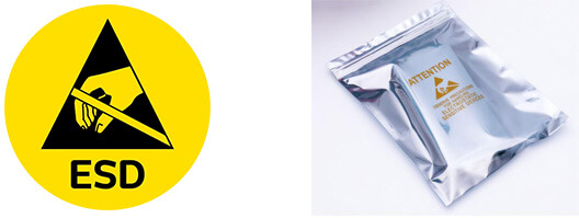
All electrostatic-sensitive components are handled in accordance with electrostatic discharge control procedures. The products are hermetically sealed in anti-static safe packaging to prevent electrostatic damage. Appropriate labeling is also applied for identification and traceability. This ensures product integrity during storage, handling and transportation.


ESD

Certifications & Memberships

Third-party certified, strict quality control. Our certification
  • ISO 9001: 2015
  • ISO 13485: 2016
  • ISO 14001: 2015
  • ISO 28000: 2007
  • ISO 45001: 2018
  • GB/T 27922-2011
  • SMTA
  • IPC
  • ESD
  • PSMA
PC28F640J3D75B TR Image

PC28F640J3D75B TR

Micron Technology Inc.
98D-PC28F640J3D75B TR

Want a better price? Add to Cart and Submit RFQ now, we'll contact you immediately.

0 RFQ
Shopping cart (0 Items)
It is empty.
Compare List (0 Items)
It is empty.
Feedback

Your feedback matters! At Allelco, we value the user experience and strive to improve it constantly.
Please share your comments with us via our feedback form, and we'll respond promptly.
Thank you for choosing Allelco.

Subject
E-mail
Comments
Captcha
Drag or click to upload file
Upload File
types: .xls, .xlsx, .doc, .docx, .jpg, .png and .pdf.
Max file size: 10MB