View All

Please refer to the English Version as our Official Version.Return

Europe
France(Français) Germany(Deutsch) Italy(Italia) Russian(русский) Poland(polski) Czech(Čeština) Luxembourg(Lëtzebuergesch) Netherlands(Nederland) Iceland(íslenska) Hungarian(Magyarország) Spain(español) Portugal(Português) Turkey(Türk dili) Bulgaria(Български език) Ukraine(Україна) Greece(Ελλάδα) Israel(עִבְרִית) Sweden(Svenska) Finland(Svenska) Finland(Suomi) Romania(românesc) Moldova(românesc) Slovakia(Slovenská) Denmark(Dansk) Slovenia(Slovenija) Slovenia(Hrvatska) Croatia(Hrvatska) Serbia(Hrvatska) Montenegro(Hrvatska) Bosnia and Herzegovina(Hrvatska) Lithuania(lietuvių) Spain(Português) Switzerland(Deutsch) United Kingdom(English)
Asia/Pacific
Japan(日本語) Korea(한국의) Thailand(ภาษาไทย) Malaysia(Melayu) Singapore(Melayu) Vietnam(Tiếng Việt) Philippines(Pilipino)
Africa, India and Middle East
United Arab Emirates(العربية) Iran(فارسی) Tajikistan(فارسی) India(हिंदी) Madagascar(malaɡasʲ)
South America / Oceania
New Zealand(Maori) Brazil(Português) Angola(Português) Mozambique(Português)
North America
United States(English) Canada(English) Haiti(Ayiti) Mexico(español)
HomeProductsIntegrated Circuits (ICs)Logic - Shift Registers74HCT595BQ,115
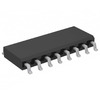
74HCT595BQ,115 Image
Image may be representation.
See specifications for product details.
EXPRESS OPTION
Payment method

74HCT595BQ,115 - Nexperia USA Inc.

Manufacturer Part Number
74HCT595BQ,115
Manufacturer
Nexperia
Allelco Part Number
98D-74HCT595BQ,115
Warranty
1 Year Allelco Warranty - Find out more
Stock Status:
8,085 pcs available, New & Original
Parts Description
IC 8BIT SHIFT REGISTER 16-DHVQFN
Package
16-DHVQFN (2.5x3.5)
Data sheet
74HCT595BQ,115.pdf
RoHs Status
ROHS3 Compliant
Our certification
In stock: 8085
  • Unit Price: $0.225
  • Subtotal: $0.00

Want a better price?
Add to Cart and Submit RFQ now, we'll contact you immediately.

Quantity Unit Price Ext. Price
1+ $0.225 $0.23
10+ $0.197 $1.97
30+ $0.185 $5.55
100+ $0.171 $17.10
500+ $0.164 $82.00
1000+ $0.159 $159.00
The above prices does not include taxes and freight rates, which will be calculated on the order pages.


Specifications

74HCT595BQ,115 Tech Specifications
Nexperia USA Inc. - 74HCT595BQ,115 technical specifications, attributes, parameters and parts with similar specifications to Nexperia USA Inc. - 74HCT595BQ,115

Product Attribute Attribute Value
Manufacturer Nexperia
Voltage - Supply 4.5V ~ 5.5V
Supplier Device Package 16-DHVQFN (2.5x3.5)
Series 74HCT
Package / Case 16-VFQFN Exposed Pad
Package Tape & Reel (TR)
Output Type Tri-State
Product Attribute Attribute Value
Operating Temperature -40°C ~ 125°C
Number of Elements 1
Number of Bits per Element 8
Mounting Type Surface Mount
Logic Type Shift Register
Function Serial to Parallel, Serial
Base Product Number 74HCT595

Environmental & Export Classifications

ATTRIBUTE DESCRIPTION
RoHs Status ROHS3 Compliant
Moisture Sensitivity Level (MSL) 1 (Unlimited)
REACH Status REACH Unaffected
ECCN EAR99
HTSUS 8542.39.0001

Frequently Asked Questions(FAQ)

How does the 74HCT595BQ,115 handle clock signal synchronization when cascading multiple shift registers in a daisy-chain configuration?
The 74HCT595BQ,115 uses a single common clock input (SH_CP) for all stages, ensuring that data shifts synchronously across all registers. When cascading, the serial output (Q7S) of one device connects to the serial input (SER) of the next, while both devices share the same SH_CP and ST_CP lines. This design guarantees that parallel loads occur simultaneously across all registers at the rising edge of ST_CP, minimizing skew and enabling reliable multi-stage control in applications such as LED matrix driving or addressable lighting systems.
What is the maximum propagation delay through the entire shift register chain in the 74HCT595BQ,115, and how does it affect high-speed digital systems?
The typical propagation delay from serial input to parallel output in the 74HCT595BQ,115 is approximately 20 ns at VCC = 5V and room temperature. For an 8-bit shift, the worst-case total latency from first bit input to final parallel output is about 160 ns. While this may seem acceptable for many applications, designers must ensure that the system clock frequency allows sufficient time between serial data shifts and parallel load operations—especially in systems requiring precise timing alignment, such as industrial motor control or real-time sensor multiplexing.
Can the 74HCT595BQ,115 drive inductive loads directly, and what precautions are necessary to prevent damage?
The 74HCT595BQ,115 outputs are not designed to drive inductive loads like relays or solenoids directly due to their limited current sourcing/sinking capability (typically ±3 mA). Inductive kickback can exceed internal voltage ratings and cause latch-up or device failure. External buffer circuits using transistors or dedicated driver ICs are required. In practice, most designs use NPN transistors with flyback diodes or MOSFET drivers to isolate the logic supply and protect the shift register.
How does the power consumption of the 74HCT5CT595BQ,115 compare to other 74HC family shift registers under dynamic switching conditions?
The 74HCT595BQ,115 consumes approximately 1 µA in static mode and up to 10 mA during active switching at 5V, depending on output load and clock frequency. Compared to standard 74HC variants, the HCT version draws slightly higher current due to TTL-compatible input thresholds but offers better noise immunity. In contrast to CMOS-only devices like the 74CBT3245, which may consume less quiescent power, the HCT series trades off efficiency for compatibility with 5V legacy systems—making it suitable where mixed-voltage environments demand robust input staging.
What is the recommended decoupling capacitor configuration for stable operation of the 74HCT595BQ,115 in high-noise industrial environments?
A 0.1 µF ceramic capacitor should be placed as close as possible to the VCC and GND pins of the 74HCT595BQ,115, preferably within 5 mm. Additionally, a 10 µF electrolytic capacitor near the board’s power entry point helps stabilize supply rails during rapid load transients. Given the device’s MSL rating of 1 and exposure to potential EMI in industrial settings, proper decoupling reduces ground bounce and minimizes false triggering on inputs like SER or OE (output enable), ensuring reliable data integrity.
How should the output enable (OE) pin be managed when using the 74HCT595BQ,115 for bidirectional communication over long traces?
The OE pin should remain asserted (low) during normal transmission to avoid floating outputs, which can cause shoot-through currents or undefined states on long traces. If tri-state functionality is needed (e.g., for bus sharing), OE must be controlled via a microcontroller with precise timing relative to data changes. However, due to trace capacitance and propagation delays, enabling/disabling outputs rapidly may result in glitches. Therefore, OE transitions should be coordinated with clock cycles to prevent bus contention in multi-device configurations.
What is the impact of temperature variation from -40°C to 125°C on the output drive strength of the 74HCT595BQ,115?
At elevated temperatures, the output voltage swing of the 74HCT595BQ,115 decreases slightly due to increased transistor resistance in the output stage. For example, VOH may drop from 4.4V at 25°C to 3.8V at 125°C when sourcing 1 mA. While still above minimum VIH thresholds for most TTL inputs, this reduction affects margin in long-chain or noisy environments. Designers targeting automotive or aerospace applications must verify that output levels remain compatible with downstream logic families across the full operating range.
How does the 74HCT595BQ,115 compare to the SN74LV595APW in terms of input threshold compatibility and power efficiency?
The 74HCT595BQ,115 uses CMOS inputs with TTL-level thresholds, allowing direct interfacing with 5V microcontrollers without level shifters. In contrast, the SN74LV595APW operates at lower voltages (2.3–3.6V) and has stricter input thresholds optimized for 3.3V logic. While the LV version consumes significantly less power (µA range), the HCT variant sacrifices efficiency for backward compatibility. For systems transitioning from 5V to 3.3V, the LV595 may reduce overall power but requires careful signal conditioning if mixed-voltage signaling is involved.
Is it safe to leave unused outputs of the 74HCT595BQ,115 unconnected, or do they require pull-up/pull-down resistors?
Unused outputs can be left unconnected without immediate risk, but they should not float indefinitely in noisy environments. Although the tri-state structure prevents leakage currents, floating nodes increase susceptibility to EMI-induced oscillations. Best practice is to tie unused outputs to VCC or GND via 10 kΩ resistors to establish defined states and improve noise immunity. This also simplifies debugging during development by ensuring predictable behavior in partial-load scenarios.
What considerations apply when routing the 16-DHVQFN package of the 74HCT595BQ,115 on a compact PCB layout?
The 16-DHVQFN (2.5x3.5 mm) exposes thermal pads on both top and bottom layers. Signal traces adjacent to the exposed pad must maintain adequate clearance (≥0.2 mm) to prevent shorting during reflow soldering. Use multiple vias under the pad to distribute heat evenly and connect directly to the inner ground plane for optimal thermal performance. Due to the small pitch (0.4 mm between pins), controlled impedance routing is unnecessary, but minimize trace length on high-speed signals like SH_CP to reduce ringing and ensure clean data capture.
Can the 74HCT595BQ,115 be used in battery-powered applications despite its relatively higher quiescent current compared to modern alternatives?
While the 74HCT595BQ,115 consumes more power than low-power CMOS shift registers (e.g., 74LVC595AQ), it remains usable in low-duty-cycle applications such as remote sensors or periodic display updates. With a typical quiescent current of 1 µA and active draw of ~10 mA, average power depends heavily on switching frequency. For instance, at 1 kHz clock rate, average current drops below 100 µA—adequate for coin-cell operation over weeks. However, continuous operation at high frequencies will quickly drain batteries, necessitating alternative IC selection for ultra-low-power designs.
How does the internal architecture of the 74HCT595BQ,115 support simultaneous shift and storage functions without data loss?
The 74HCT595BQ,115 integrates a master latch that holds shifted data independently of ongoing serial input. During shifting, data flows into the shift register; once eight bits are loaded, asserting ST_CP transfers the latched content to the output register. This separation ensures that new data can continue shifting in while previous data is held steady for parallel output—critical for real-time systems where continuous serial streaming must coexist with stable peripheral actuation without interruption.
What is the effect of VCC ripple exceeding ±5% on the 74HCT595BQ,115’s output stability?
Excessive VCC ripple beyond ±5% can cause erratic behavior, particularly on the OE or ST_CP lines, due to insufficient headroom for noise margins. At 5V nominal, a ripple peak-to-peak of >100 mV may lead to unintended output toggling or incomplete parallel loads. In sensitive applications like precision DAC interfacing or regulated power sequencing, adding LC filters or using linear regulators improves PSRR and ensures consistent operation, especially when driving capacitive loads that exacerbate supply droop.
How does the 74HCT595BQ,115 interface with I²C-based expansion buses in multi-master systems?
Direct connection is impractical because the 74HCT595BQ,115 lacks open-drain outputs required for wired-AND bus protocols. Instead, it should not share the same bus line unless isolated via buffers. However, it can serve as an I/O expander controlled via SPI or GPIOs from an I²C master, effectively decoupling communication domains. This indirect approach avoids contention while leveraging the shift register’s strength in expanding parallel outputs without additional address decoding overhead.
What are the implications of using the 74HCT595BQ,115 in ESD-sensitive environments without external protection?
Although the device includes basic human-body model (HBM) ESD protection (±2 kV), industrial environments often exceed this. Without external TVS diodes or clamping circuits near connectors, transient events from cables or handling can compromise reliability. Implementing ESD protection at every interface—especially on SER and SH_CP lines—extends lifetime and prevents latent failures in field-deployed equipment, particularly where maintenance access is limited or environmental stresses are high.

Parts with Similar Specifications

The three parts on the right have similar specifications to Nexperia USA Inc. 74HCT595BQ,115

Product Attribute 74HCT595BQ-Q100,11 74HCT595D-Q100,118 74HCT594DB,118 74HCT595D,112
Part Number 74HCT595BQ-Q100,11 74HCT595D-Q100,118 74HCT594DB,118 74HCT595D,112
Manufacturer Nexperia USA Inc. Nexperia USA Inc. NXP USA Inc. NXP Semiconductors
Base Product Number - DAC34H84 MAX500 ADS62P42
Number of Elements - - - -
Supplier Device Package - 196-NFBGA (12x12) 16-PDIP 64-VQFN (9x9)
Operating Temperature - -40°C ~ 85°C 0°C ~ 70°C -40°C ~ 85°C
Package - Tape & Reel (TR) Tube Tape & Reel (TR)
Number of Bits per Element - - - -
Voltage - Supply - - - -
Function - - - -
Output Type - Current - Unbuffered Voltage - Buffered -
Package / Case - 196-LFBGA 16-DIP (0.300', 7.62mm) 64-VFQFN Exposed Pad
Logic Type - - - -
Series - - - -
Mounting Type - Surface Mount Through Hole Surface Mount

74HCT595BQ,115 Datasheet PDF

Download 74HCT595BQ,115 pdf datasheets and Nexperia USA Inc. documentation for 74HCT595BQ,115 - Nexperia USA Inc..

PCN Packaging
Label Chg 12/Mar/2017.pdf All Dev Label Chgs 2/Aug/2020.pdf
PCN Assembly/Origin
Wafer Fab 24/Dec/2020.pdf

Customer Reviews

Evaluation: 10 Articles

  • ECUb***h
    Sep 22, 2026

    Used for repair of an older automotive ECU. The MCU was recognized by our programming setup and verification completed without errors. The repaired board now starts and communicates normally.

  • RS48***ieldTech
    Sep 16, 2026

    Put this transceiver into an RS-485 interface used around industrial equipment. Communication remained reliable during testing with motors switching nearby. Good result for the replacement board.

  • Logi***b_Chris
    Sep 8, 2026

    Purchased for a Cyclone III development project. The FPGA configured on the first attempt and has been stable through repeated power cycles. No problems with the I/O we are using.

  • Circ***FixerTom
    Sep 2, 2026

    Used this rectifier in a high-current power supply repair. Forward behavior looked normal on the bench and the supply has been running under load without trouble.

  • Retr***UWorks
    Aug 31, 2026

    Needed the exact ST10F269Z2Q6 for servicing an older control unit. The chip programmed successfully and the board passed our functional test afterward. Much easier than redesigning around a newer MCU.

  • Andr***PCBLab
    Aug 28, 2026

    I needed this ADC for an older data acquisition board. Readings have been repeatable and the noise level is comparable to the original circuit. Happy with the purchase.

  • Leat***O'Keefe
    Aug 20, 2026

    one of my hobbies is skydiving. and when i'm skydiving this works great.

  • Ilen***
    Aug 20, 2026

    This product works considerably well. It secretly improves my basketball by a lot.

  • Indu***ialPower
    Aug 17, 2026

    Installed this IGBT module in a power conversion cabinet. Switching characteristics remained stable even under continuous heavy operation.

  • Nikh***ech
    Aug 13, 2026

    Great low-power MCU for portable equipment. Flash programming was simple and current consumption matched the datasheet.

Write a Review

Your Email address will not be published.

Shipment

Delivery Time

In-stock items can be shipped within 24 hours. Some parts will be arranged for delivery within 1-2 days from the date all items arrive at our warehouse. And Allelco ships order once a day at about 17:00, except Sunday. Once the goods are shipped, the estimated delivery time depends on the shipping methods and Delivery destination. The table below shows are the logistic time for some common countries.

Delivery Cost

  1. Use your express account for shipment if you have one.
  2. Use our account for the shipment. Refer to the table below for the approximate charges.
(Different time frame / countries / package size has different price.)

Delivery Method

  1. Global Common Shipment by DHL / UPS / FedEx / TNT / EMS / SF we support.
  2. Others more shipping ways, please get in touch with your customer manager.

Common Countries Logistic Time Reference
Region Country Logistic Time(Day)
America United States 5
Brazil 7
Europe Germany 5
United Kingdom 4
Italy 5
Oceania Australia 6
New Zealand 5
Asia India 4
Japan 4
Middle East Israel 6
DHL & FedEx Shipment Charges Reference
Shipment charges(KG) Reference DHL(USD$)
0.00kg-1.00kg USD$30.00 - USD$60.00
1.00kg-2.00kg USD$40.00 - USD$80.00
2.00kg-3.00kg USD$50.00 - USD$100.00
Note:
The above table is for reference only. There may have some data bias for the uncontrollable factors.
Contact us if you have any questions.
  • QC (Quality Warranty)
  • Payment Support
  • Packaging
  • Certifications & Memberships

QC (Quality Warranty)

Allelco is committed to exceeding customer expectations through customer service excellence, order accuracy, and on-time delivery.
This is achieved through our commitment to the continual improvement of our processes, services, and products.


Strict quality inspection builds a solid foundation for electronic component quality.
  1. Visual inspection
  2. Performance testing and reliability verification
  3. Standardized full-process testing
  4. Precise control of every parameter
We eliminate defective components and ensure the stable operation of electronic devices through professional quality standards.

Payment Support

The payment method can be chosen from the methods shown below: Wire Transfer (T/T, Bank Transfer), Western Union, Credit card, PayPal.
  • HKBea
  • Paypal
  • MasterCard
  • Western-Union
  • VISA
Stable Delivery, Sincere Partnership — Your Faithful Supply Chain Partner
  • Efficient Supply Management
  • Cost-Saving Procurement
  • Fast Sourcing & Delivery
Contact us if you have any questions.

Packaging

Electrostatic Discharge Protection and Handling

All electrostatic-sensitive components are handled in accordance with electrostatic discharge control procedures. The products are hermetically sealed in anti-static safe packaging to prevent electrostatic damage. Appropriate labeling is also applied for identification and traceability. This ensures product integrity during storage, handling and transportation.


ESD

Certifications & Memberships

Third-party certified, strict quality control. Our certification
  • ISO 9001: 2015
  • ISO 13485: 2016
  • ISO 14001: 2015
  • ISO 28000: 2007
  • ISO 45001: 2018
  • GB/T 27922-2011
  • SMTA
  • IPC
  • ESD
  • PSMA
74HCT595BQ,115 Image

74HCT595BQ,115

Nexperia USA Inc.
98D-74HCT595BQ,115

Want a better price? Add to Cart and Submit RFQ now, we'll contact you immediately.

0 RFQ
Shopping cart (0 Items)
It is empty.
Compare List (0 Items)
It is empty.
Feedback

Your feedback matters! At Allelco, we value the user experience and strive to improve it constantly.
Please share your comments with us via our feedback form, and we'll respond promptly.
Thank you for choosing Allelco.

Subject
E-mail
Comments
Captcha
Drag or click to upload file
Upload File
types: .xls, .xlsx, .doc, .docx, .jpg, .png and .pdf.
Max file size: 10MB