View All

Please refer to the English Version as our Official Version.Return

Europe
France(Français) Germany(Deutsch) Italy(Italia) Russian(русский) Poland(polski) Czech(Čeština) Luxembourg(Lëtzebuergesch) Netherlands(Nederland) Iceland(íslenska) Hungarian(Magyarország) Spain(español) Portugal(Português) Turkey(Türk dili) Bulgaria(Български език) Ukraine(Україна) Greece(Ελλάδα) Israel(עִבְרִית) Sweden(Svenska) Finland(Svenska) Finland(Suomi) Romania(românesc) Moldova(românesc) Slovakia(Slovenská) Denmark(Dansk) Slovenia(Slovenija) Slovenia(Hrvatska) Croatia(Hrvatska) Serbia(Hrvatska) Montenegro(Hrvatska) Bosnia and Herzegovina(Hrvatska) Lithuania(lietuvių) Spain(Português) Switzerland(Deutsch) United Kingdom(English)
Asia/Pacific
Japan(日本語) Korea(한국의) Thailand(ภาษาไทย) Malaysia(Melayu) Singapore(Melayu) Vietnam(Tiếng Việt) Philippines(Pilipino)
Africa, India and Middle East
United Arab Emirates(العربية) Iran(فارسی) Tajikistan(فارسی) India(हिंदी) Madagascar(malaɡasʲ)
South America / Oceania
New Zealand(Maori) Brazil(Português) Angola(Português) Mozambique(Português)
North America
United States(English) Canada(English) Haiti(Ayiti) Mexico(español)
HomeProductsIntegrated Circuits (ICs)Specialized ICs74HCT595D
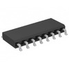
74HCT595D Image
Image may be representation.
See specifications for product details.
EXPRESS OPTION
Payment method

74HCT595D - Nexperia

Manufacturer Part Number
74HCT595D
Manufacturer
Nexperia
Allelco Part Number
32D-74HCT595D
Warranty
1 Year Allelco Warranty - Find out more
Stock Status:
15,320 pcs available, New & Original
Parts Description
DAC91001
Data sheet
-
Category
Integrated Circuits (ICs) > Specialized ICs
RoHs Status
Our certification
In stock: 15320

Required fields are indicated by an asterisk (*)
Please send RFQ, we will respond immediately.

Quantity

Specifications

74HCT595D Tech Specifications
Nexperia - 74HCT595D technical specifications, attributes, parameters and parts with similar specifications to Nexperia - 74HCT595D

Product Attribute Attribute Value
Part Number 74HCT595D
Package DAC91001
Description DAC91001
Stock Condition Get 15320 pcs available quantity at Allelco
Payment PayPal / TT / Credit Card / Western Union
Allelco Certifications ESD / ISO 9001 / ISO 13485 / ISO 28000
Product Attribute Attribute Value
Manufacturer Nexperia
RoHs Status -
Warranty 100% Perfect Functions
Transport port Hong Kong
Shipping by DHL / FedEx / UPS / TNT / SF Express
RFQ Email info@allelco.com

Frequently Asked Questions(FAQ)

What is the recommended operating voltage range for the NEXPERIA 74HCT595D shift register to ensure reliable data transmission without risk of latch-up?
The 74HCT595D is designed to operate reliably within a supply voltage range of 4.5 V to 5.5 V. Operating outside this range may lead to undefined logic levels or potential damage due to overvoltage conditions. For stable performance in 5V digital systems, the recommended nominal supply is 5.0 V ±5%, which ensures proper input and output thresholds compatible with standard TTL and CMOS logic families.
How does the propagation delay of the 74HCT595D compare between high-to-low and low-to-high output transitions, and what impact does this have on synchronous system timing?
The 74HCT595D exhibits a typical propagation delay (tPHL and tPLH) of approximately 12 ns at 5.0 V and 25°C. While both delays are closely matched, slight asymmetry can occur due to internal transistor characteristics. In high-speed clocked applications, cumulative skew across multiple stages must be considered. For a 16-bit shift register chain, total delay could reach ~200 ns, potentially affecting setup and hold margins in tightly timed serial communication protocols.
Can the 74HCT595D be used in a cascaded configuration with other shift registers, and what precautions should be taken regarding output enable and clear functionality?
Yes, the 74HCT595D supports cascading via its serial input (SER), storage register clock (STCP), and shift register clock (SHCP) pins. However, when multiple devices are chained, care must be taken to synchronize the STCP signal across all units to prevent partial updates. Additionally, the master reset (MR) pin should be tied to a common active-low reset line to ensure all registers initialize consistently. Avoid floating MR; use a pull-up resistor if unused.
What is the maximum allowable sink current per output pin of the 74HCT595D, and how does this limit load-driving capability in LED matrix applications?
Each output pin of the 74HCT595D can safely sink up to 25 mA continuously. With eight outputs active simultaneously, total package power dissipation must remain below 150 mW to avoid thermal shutdown. For driving LEDs in a multiplexed display, individual current limiting resistors should ensure each pin operates well under 20 mA to maintain reliability and color consistency over time.
How does temperature affect the input threshold voltages of the 74HCT595D, and what implications does this have for noise immunity in industrial environments?
The input high voltage (VIH) minimum is specified at 3.15 V at 4.5 V supply and 2.0 V at 5.5 V, with typical hysteresis around 0.1–0.3 V. Over the commercial temperature range (-40°C to +85°C), these thresholds may shift slightly due to semiconductor doping variations. In electrically noisy environments, this small hysteresis helps reject glitches below 1.0 V, but designers should ensure that noise peaks do not exceed VIH(min) during transient events such as motor commutation or relay switching.
Is it acceptable to leave unused inputs of the 74HCT595D unconnected, and what risks arise from improper handling of the OE, MR, and SER pins during prototyping?
No, unused control inputs—particularly OE (output enable) and MR (master reset)—should never be left floating. The OE pin defaults high when floating, disabling outputs and causing unintended power savings. Similarly, leaving MR floating risks erratic initialization. SER, being an input, may pick up noise; connect it to GND via a 10 kΩ resistor if not used. Always adhere to manufacturer guidelines for open-drain or tri-state pin management to prevent latch-up or oscillation.
What is the difference in power consumption between quiescent and full-output-drive conditions for the 74HCT595D, and how might this affect battery-powered designs?
At 5.0 V and 25°C, the 74HCT595D consumes approximately 8 µA in quiescent mode with no clocks applied. However, when driving heavy capacitive loads or sourcing/sinking significant current (e.g., multiple LEDs), dynamic power increases proportionally to switching frequency and load. In low-power applications, minimizing clock rate and using output enable to gate updates can reduce average current draw by up to 90%, extending battery life in portable instrumentation.
How does the 74HCT595D handle bus contention when sharing a common output line with another device, and what protection features are inherent to the design?
The 74HCT595D does not support true wired-OR or bidirectional operation. If two outputs drive the same net simultaneously with mismatched logic states, excessive current flows through parasitic diodes and output transistors, potentially exceeding absolute maximum ratings. Although built-in ESD protection exists, continuous contention violates safe operating conditions. Therefore, external isolation such as series resistors or open-collector buffers should be employed when sharing lines in multi-device systems.
In what scenarios would the 74HCT595D outperform alternatives like the 74HC595 or 74LVC595, particularly regarding fan-out and voltage translation?
The 74HCT595D offers superior compatibility with 5V TTL logic families, making it ideal for legacy system upgrades or mixed-voltage interfaces where 3.3V MCUs drive older 5V peripherals. Compared to the 74HC595, it has slightly higher input leakage and reduced noise margin at lower supplies, but better VIH/VIL matching with 5V systems. Against the 74LVC595, the HCT variant provides stronger drive strength at 5V while maintaining CMOS efficiency—useful in applications requiring direct interface without level shifters, such as retrofitting displays into vintage equipment.
What are the key differences in slew rate and rise/fall times between the 74HCT595D and modern LVCMOS variants, and how does this influence EMI performance in long PCB traces?
The 74HCT595D typically exhibits rise and fall times of 5–8 ns under 5V operation, resulting in a moderate slew rate that balances speed and EMI. Faster edges than slower CMOS devices, but less aggressively damped than LVDS or CML outputs. On long interconnects, this can generate measurable radiated emissions above 100 MHz. Adding series termination resistors near drivers or using spread-spectrum clocking can mitigate ringing and reduce electromagnetic interference in compliance-critical designs.
Can the 74HCT595D directly drive inductive loads like relays without additional circuitry, and what failure mechanisms should be anticipated?
No, the 74HCT595D cannot directly energize inductive loads such as solenoids or relays. Inductive kickback will reverse-bias output protection diodes, allowing flyback current to flow back into the IC, potentially exceeding junction limits and causing permanent damage. A flyback diode across the load and a series current-limiting resistor are mandatory. Alternatively, use a buffer transistor rated for coil current to isolate the shift register from inductive transients.
How does the internal structure of the 74HCT595D’s storage register differ from its shift register, and why is dual-edge operation not supported?
The 74HCT595D contains two distinct registers: a 8-bit shift register and a separate 8-bit storage register. Data shifts on the rising edge of SHCP, while the storage register latches all bits simultaneously on the rising edge of STCP. This architecture enables pipelined operation but does not allow data transfer on both edges of either clock. Dual-edge operation would require complex edge detection logic not implemented in this synchronous design, limiting maximum usable clock frequency to half the reciprocal of total cycle time including latch delay.
What is the significance of the 74HCT595D’s output disable feature, and how can it be leveraged to reduce crosstalk in multi-layer PCBs?
When OE (Output Enable) is asserted high, all Q outputs enter a high-impedance state, effectively disconnecting the shift register from downstream circuits. This reduces capacitive coupling between adjacent signal layers and minimizes ground bounce during inactive periods. In dense layouts with many shift registers, selectively enabling only one at a time using OE controlled by a decoder can suppress crosstalk and improve signal integrity—especially beneficial in matrix addressing schemes where multiple rows or columns are not active simultaneously.
Are there any known limitations in using the 74HCT595D with high-impedance sensor interfaces or analog multiplexers?
While the 74HCT595D itself is digital, connecting its outputs directly to high-impedance analog nodes (e.g., ADC inputs or op-amp feedback paths) risks loading effects and charge injection during switching. The output capacitance (typically 15 pF) combined with source impedance can form an RC filter that attenuates slow-changing signals. For precision analog applications, consider isolating digital outputs with buffers or using dedicated analog switches instead of repurposing shift registers for signal routing.
How does the 74HCT595D perform under rapid clocking near its maximum frequency, and what derating factors should inform real-world design choices?
The 74HCT595D specifies a maximum clock frequency of 38 MHz at 5.0 V and 25°C. However, real-world performance degrades with temperature, supply droop, and load capacitance. Near 35 MHz, timing margins shrink significantly, increasing risk of metastability if data arrives too close to clock edges. To ensure robustness, limit actual operating frequency to 70% of spec, add guard bands for process variation, and verify worst-case timing with SPICE models or oscilloscope measurements under full load.
What role does the master reset (MR) pin play during power-up sequencing, and how does it interact with internal bias circuits?
The MR pin actively resets all flip-flops in both the shift and storage registers when pulled low. During power-up, asserting MR early ensures deterministic initial state before clocks are applied. Internally, the MR circuit includes a Schmitt trigger to reject glitches, but prolonged undershoot below -0.3 V may violate absolute maximum ratings. Best practice is to use a resistor-divider network to generate a delayed reset pulse that holds MR low until VCC stabilizes above 3.0 V, preventing accidental resets during brownout conditions.
In automotive-grade designs, could environmental stressors impact the 74HCT595D’s long-term reliability, and are there mitigation strategies beyond standard commercial ratings?
Although the 74HCT595D is rated for -40°C to +85°C, automotive applications often demand operation up to +125°C with elevated humidity and vibration. Thermal cycling accelerates solder joint fatigue and dielectric degradation. To enhance reliability, mount the SOP16 package with adequate copper pour and thermal relief pads, avoid soldering near leads during reflow, and consider conformal coating to protect against moisture ingress. Where possible, select automotive-qualified equivalents with AEC-Q100 certification instead of relying solely on commercial parts.
How does the pinout of the 74HCT595D facilitate integration into space-constrained PCBs, and what layout considerations maximize performance?
The 74HCT595D uses a standard SOP16 footprint with mirrored pin numbering, placing power (VCC and GND) on opposite ends and control signals centrally. This symmetry aids routing in compact designs. To minimize inductance and crosstalk, place decoupling capacitors (<100 nF ceramic) as close as possible to VCC and GND pins, route clock and data lines differentially if possible, and keep OE and MR traces short and away from high-current paths. Ground plane stitching under the package further reduces loop area and improves noise immunity.

Customer Reviews

Evaluation: 10 Articles

  • ECUb***h
    Sep 22, 2026

    Used for repair of an older automotive ECU. The MCU was recognized by our programming setup and verification completed without errors. The repaired board now starts and communicates normally.

  • RS48***ieldTech
    Sep 16, 2026

    Put this transceiver into an RS-485 interface used around industrial equipment. Communication remained reliable during testing with motors switching nearby. Good result for the replacement board.

  • Logi***b_Chris
    Sep 8, 2026

    Purchased for a Cyclone III development project. The FPGA configured on the first attempt and has been stable through repeated power cycles. No problems with the I/O we are using.

  • Circ***FixerTom
    Sep 2, 2026

    Used this rectifier in a high-current power supply repair. Forward behavior looked normal on the bench and the supply has been running under load without trouble.

  • Retr***UWorks
    Aug 31, 2026

    Needed the exact ST10F269Z2Q6 for servicing an older control unit. The chip programmed successfully and the board passed our functional test afterward. Much easier than redesigning around a newer MCU.

  • Andr***PCBLab
    Aug 28, 2026

    I needed this ADC for an older data acquisition board. Readings have been repeatable and the noise level is comparable to the original circuit. Happy with the purchase.

  • Leat***O'Keefe
    Aug 20, 2026

    one of my hobbies is skydiving. and when i'm skydiving this works great.

  • Ilen***
    Aug 20, 2026

    This product works considerably well. It secretly improves my basketball by a lot.

  • Indu***ialPower
    Aug 17, 2026

    Installed this IGBT module in a power conversion cabinet. Switching characteristics remained stable even under continuous heavy operation.

  • Nikh***ech
    Aug 13, 2026

    Great low-power MCU for portable equipment. Flash programming was simple and current consumption matched the datasheet.

Write a Review

Your Email address will not be published.

Shipment

Delivery Time

In-stock items can be shipped within 24 hours. Some parts will be arranged for delivery within 1-2 days from the date all items arrive at our warehouse. And Allelco ships order once a day at about 17:00, except Sunday. Once the goods are shipped, the estimated delivery time depends on the shipping methods and Delivery destination. The table below shows are the logistic time for some common countries.

Delivery Cost

  1. Use your express account for shipment if you have one.
  2. Use our account for the shipment. Refer to the table below for the approximate charges.
(Different time frame / countries / package size has different price.)

Delivery Method

  1. Global Common Shipment by DHL / UPS / FedEx / TNT / EMS / SF we support.
  2. Others more shipping ways, please get in touch with your customer manager.

Common Countries Logistic Time Reference
Region Country Logistic Time(Day)
America United States 5
Brazil 7
Europe Germany 5
United Kingdom 4
Italy 5
Oceania Australia 6
New Zealand 5
Asia India 4
Japan 4
Middle East Israel 6
DHL & FedEx Shipment Charges Reference
Shipment charges(KG) Reference DHL(USD$)
0.00kg-1.00kg USD$30.00 - USD$60.00
1.00kg-2.00kg USD$40.00 - USD$80.00
2.00kg-3.00kg USD$50.00 - USD$100.00
Note:
The above table is for reference only. There may have some data bias for the uncontrollable factors.
Contact us if you have any questions.
  • QC (Quality Warranty)
  • Payment Support
  • Packaging
  • Certifications & Memberships

QC (Quality Warranty)

Allelco is committed to exceeding customer expectations through customer service excellence, order accuracy, and on-time delivery.
This is achieved through our commitment to the continual improvement of our processes, services, and products.


Strict quality inspection builds a solid foundation for electronic component quality.
  1. Visual inspection
  2. Performance testing and reliability verification
  3. Standardized full-process testing
  4. Precise control of every parameter
We eliminate defective components and ensure the stable operation of electronic devices through professional quality standards.

Payment Support

The payment method can be chosen from the methods shown below: Wire Transfer (T/T, Bank Transfer), Western Union, Credit card, PayPal.
  • HKBea
  • Paypal
  • MasterCard
  • Western-Union
  • VISA
Stable Delivery, Sincere Partnership — Your Faithful Supply Chain Partner
  • Efficient Supply Management
  • Cost-Saving Procurement
  • Fast Sourcing & Delivery
Contact us if you have any questions.

Packaging

Electrostatic Discharge Protection and Handling

All electrostatic-sensitive components are handled in accordance with electrostatic discharge control procedures. The products are hermetically sealed in anti-static safe packaging to prevent electrostatic damage. Appropriate labeling is also applied for identification and traceability. This ensures product integrity during storage, handling and transportation.


ESD

Certifications & Memberships

Third-party certified, strict quality control. Our certification
  • ISO 9001: 2015
  • ISO 13485: 2016
  • ISO 14001: 2015
  • ISO 28000: 2007
  • ISO 45001: 2018
  • GB/T 27922-2011
  • SMTA
  • IPC
  • ESD
  • PSMA
74HCT595D Image

74HCT595D

Nexperia
32D-74HCT595D

Want a better price? Add to Cart and Submit RFQ now, we'll contact you immediately.

0 RFQ
Shopping cart (0 Items)
It is empty.
Compare List (0 Items)
It is empty.
Feedback

Your feedback matters! At Allelco, we value the user experience and strive to improve it constantly.
Please share your comments with us via our feedback form, and we'll respond promptly.
Thank you for choosing Allelco.

Subject
E-mail
Comments
Captcha
Drag or click to upload file
Upload File
types: .xls, .xlsx, .doc, .docx, .jpg, .png and .pdf.
Max file size: 10MB