View All

Please refer to the English Version as our Official Version.Return

Europe
France(Français) Germany(Deutsch) Italy(Italia) Russian(русский) Poland(polski) Czech(Čeština) Luxembourg(Lëtzebuergesch) Netherlands(Nederland) Iceland(íslenska) Hungarian(Magyarország) Spain(español) Portugal(Português) Turkey(Türk dili) Bulgaria(Български език) Ukraine(Україна) Greece(Ελλάδα) Israel(עִבְרִית) Sweden(Svenska) Finland(Svenska) Finland(Suomi) Romania(românesc) Moldova(românesc) Slovakia(Slovenská) Denmark(Dansk) Slovenia(Slovenija) Slovenia(Hrvatska) Croatia(Hrvatska) Serbia(Hrvatska) Montenegro(Hrvatska) Bosnia and Herzegovina(Hrvatska) Lithuania(lietuvių) Spain(Português) Switzerland(Deutsch) United Kingdom(English)
Asia/Pacific
Japan(日本語) Korea(한국의) Thailand(ภาษาไทย) Malaysia(Melayu) Singapore(Melayu) Vietnam(Tiếng Việt) Philippines(Pilipino)
Africa, India and Middle East
United Arab Emirates(العربية) Iran(فارسی) Tajikistan(فارسی) India(हिंदी) Madagascar(malaɡasʲ)
South America / Oceania
New Zealand(Maori) Brazil(Português) Angola(Português) Mozambique(Português)
North America
United States(English) Canada(English) Haiti(Ayiti) Mexico(español)
HomeProductsIntegrated Circuits (ICs)Linear - Amplifiers - AudioTDA75610S-ZST
TDA75610S-ZST Image
Image may be representation.
See specifications for product details.
EXPRESS OPTION
Payment method

TDA75610S-ZST - STMicroelectronics

Manufacturer Part Number
TDA75610S-ZST
Manufacturer
STMicroelectronics
Allelco Part Number
32D-TDA75610S-ZST
Warranty
1 Year Allelco Warranty - Find out more
Stock Status:
6,831 pcs available, New & Original
Parts Description
IC AMP AB QUAD 45W POWERSO-36
Package
PowerSO-36
Data sheet
TDA75610S-ZST.pdf
RoHs Status
ROHS3 Compliant
Our certification
In stock: 6831

Required fields are indicated by an asterisk (*)
Please send RFQ, we will respond immediately.

Quantity

Specifications

TDA75610S-ZST Tech Specifications
STMicroelectronics - TDA75610S-ZST technical specifications, attributes, parameters and parts with similar specifications to STMicroelectronics - TDA75610S-ZST

Product Attribute Attribute Value
Manufacturer STMicroelectronics
Voltage - Supply 6V ~ 18V
Type Class AB
Supplier Device Package PowerSO-36
Series -
Package / Case PowerSO-36 Exposed Bottom Pad
Package Tape & Reel (TR)
Product Attribute Attribute Value
Output Type 4-Channel (Quad)
Operating Temperature -40°C ~ 105°C (TA)
Mounting Type Surface Mount
Max Output Power x Channels @ Load 45W x 4 @ 4Ohm
Features Mute, Standby
Base Product Number TDA75610

Environmental & Export Classifications

ATTRIBUTE DESCRIPTION
RoHs Status ROHS3 Compliant
Moisture Sensitivity Level (MSL) 3 (168 Hours)
REACH Status REACH Unaffected
ECCN EAR99

Parts Introduction

TDA75610S-ZST Image
TDA75610S-ZST (1)

Manufacturer Part Number

TDA75610S-ZST

Manufacturer

STMicroelectronics

Introduction

High-performance quad-channel audio power amplifier integrated circuit

Designed for automotive and consumer audio applications

Product Features and Performance

4-channel operation

High output power: 45W x 4 @ 4Ohm

Class AB operation

Wide supply voltage range: 6V to 18V

Low quiescent current

Mute and standby features

Thermal protection

Short-circuit and overload protection

Product Advantages

Excellent audio quality and efficiency

Flexible supply voltage range

Comprehensive protection features

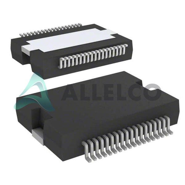
Compact PowerSO-36 package

Key Technical Parameters

Output Power: 45W x 4 @ 4Ohm

Supply Voltage Range: 6V to 18V

Operating Temperature Range: -40°C to 105°C

Quality and Safety Features

ROHS3 compliant

Thermal protection

Short-circuit and overload protection

Compatibility

Suitable for automotive and consumer audio applications

Application Areas

Car audio systems

Home audio systems

Professional audio equipment

Product Lifecycle

Current product, no plans for discontinuation

Replacement parts and upgrades available

Key Reasons to Choose This Product

High output power and efficiency

Wide supply voltage range

Comprehensive protection features

Compact and thermally efficient package

Proven reliability and performance in automotive and consumer audio applications

Frequently Asked Questions(FAQ)

How does the TDA75610S-ZST handle thermal performance when driving a 4Ω load at full output power, and what design considerations are necessary to maintain junction temperature within safe limits?
The TDA75610S-ZST delivers up to 45W per channel into a 4Ω load, resulting in significant power dissipation. At maximum output, each channel can dissipate approximately 20–25W internally due to efficiency limitations of Class AB amplifiers. With a PowerSO-36 package featuring an exposed bottom pad, thermal resistance from junction to ambient (θJA) is typically around 20–25°C/W under natural convection. This implies a temperature rise of over 400°C above ambient under worst-case conditions—far exceeding the 105°C maximum operating junction temperature. Therefore, effective heatsinking or forced airflow is essential. Engineers must ensure adequate copper area on the PCB, use thermal vias, and consider derating output power when operating near ambient temperatures above 50°C.
Can the TDA75610S-ZST be used in a stereo configuration by disabling one or two channels, and how does this affect overall system efficiency and heat generation?
Yes, the TDA75610S-ZST supports flexible channel operation through its mute and standby features. Disabling unused channels via control inputs reduces quiescent current and minimizes idle power consumption. In a stereo setup using only two of the four channels, total system power draw decreases significantly, improving overall efficiency. However, even with half the channels active, the amplifier may still operate near peak dissipation if delivering high output levels into low-impedance loads. Thermal management remains critical, as the remaining active channels will experience similar localized heating. Proper layout and thermal planning should account for worst-case single-channel operation rather than assuming uniform distribution across all four channels.
What voltage supply range and stability requirements apply to the TDA75610S-ZST to ensure reliable operation without clipping or distortion?
The TDA75610S-ZST operates reliably within a supply voltage range of 6V to 18V, making it suitable for both automotive 12V systems and higher-voltage industrial applications. To avoid headroom loss and prevent clipping, a minimum of 2V between supply rail and peak output voltage is recommended—this implies a practical ceiling of ~16V for clean 18V rails. Supply decoupling is critical; use low-ESR capacitors (e.g., 10µF tantalum or ceramic) placed within 10mm of each VCC pin to suppress high-frequency noise. Voltage ripple should remain below 200mV peak-to-peak to maintain THD+N below 0.1% at moderate outputs. Instability or droop during transient loads can cause audible artifacts or internal latch-up, so bulk capacitance and localized filtering are strongly advised.
How does the TDA75610S-ZST compare to other quad Class AB amplifiers like the TDA75600 series in terms of efficiency, output power, and integration features?
Compared to the TDA75600 family, the TDA75610S-ZST offers improved output power density—delivering 45W per channel into 4Ω versus typically 30–35W for earlier variants. Both share similar supply ranges (8–18V) and feature mute/standby functionality. However, the TDA75610 integrates more robust protection circuitry, including advanced thermal shutdown and short-circuit resilience. Efficiency-wise, both operate at ~60–65% at 50% output power into 4Ω, but the TDA75610S-ZST achieves better linearity and lower crosstalk due to refined biasing networks. While the TDA75600 may suffice for lower-power audio systems, the TDA75610S-ZST provides greater margin for demanding applications such as car audio aftermarket or professional sound reinforcement where sustained high output is required.
Is it acceptable to operate the TDA75610S-ZST near its maximum specified supply voltage (e.g., 18V) while delivering high output levels, and what risks should engineers evaluate?
Operating near 18V supply with high output into resistive loads increases stress on internal pass elements and raises quiescent current slightly, contributing to elevated power dissipation. While the device is rated for continuous operation at 18V, prolonged exposure to full supply voltage with high signal levels can accelerate aging of input stages and reduce long-term reliability. Additionally, output swing approaches rail limits, increasing harmonic distortion and intermodulation products. Engineers should perform worst-case thermal simulations and include safety margins in supply design—ideally limiting sustained operation to ≤16V unless ambient cooling is guaranteed. Monitoring die temperature via external sensors may be prudent in mission-critical systems.
What layout guidelines are essential when designing a PCB for the TDA75610S-ZST to minimize EMI, crosstalk, and thermal resistance?
The PowerSO-36 package’s exposed pad must be soldered directly to a large copper pour acting as a ground plane and heat spreader. Use multiple thermal vias (minimum eight, 0.3mm diameter) connecting the pad to an inner or bottom-layer ground plane to enhance heat dissipation and stabilize reference potential. High-current traces (supply and output) should be wide (≥30 mil) and short to reduce inductance and resistive losses. Separate analog and digital grounds, connect them at a single point near the IC, and route feedback resistors close to the input pins to preserve gain accuracy. Output traces must be routed away from sensitive input lines to prevent capacitive coupling. Follow STMicroelectronics’ recommended land pattern precisely to avoid solder voids and mechanical stress.
How does the TDA75610S-ZST handle startup transients, and what external components are needed to prevent pop or click sounds during power cycling?
The TDA75610S-ZST includes built-in mute circuitry controlled via the MUTE pin. To eliminate audible pops, a soft-start sequence must be implemented externally. A simple RC network (e.g., 10kΩ resistor and 10µF capacitor) connected between MUTE and GND creates a ~100ms delay before enabling the amplifier after power stabilization. Alternatively, use a microcontroller-driven enable line with delayed assertion. Ensure that supply voltage ramps up slowly (<10ms) using a PTC thermistor or active precharge circuit to avoid inrush current spikes. Without proper sequencing, sudden enablement can drive output stages into nonlinear regions momentarily, producing audible artifacts.
Can the TDA75610S-ZST drive inductive loads such as speakers with voice coils above 4Ω, and what precautions are necessary?
Yes, the TDA75610S-ZST can drive impedances down to 3Ω (as specified in some parametric tests), but driving higher-impedance loads (e.g., 8Ω or speaker voice coils with inductance) is permissible and often preferred for reduced current demand and improved efficiency. Inductive loads do not damage the amplifier under normal conditions, but rapid switching of DC offset or fault conditions could induce back-EMF. Include flyback diodes across relay contacts if switching speakers dynamically, and ensure output filters (if used) have sufficient damping factor to prevent oscillations. At higher impedances, output power decreases proportionally (e.g., ~20W into 8Ω at 18V), which may still meet application needs while reducing thermal load.
What role does the base product number TDA75610 play in compatibility with evaluation boards and reference designs, and how does the ZST suffix affect sourcing?
The base model TDA75610 refers to the core amplifier architecture used in multiple packaging variants. Evaluation boards and STMicroelectronics reference designs (e.g., STEVAL-SAM003V1) are typically compatible across these packages. The ZST suffix denotes a specific tape-and-reel format (Cut Tape and Digi-Reel®) compliant with JEDEC standards for automated assembly. While functional behavior remains identical to other ZST-coded versions, procurement logistics differ—ZST ensures compatibility with high-volume SMT lines. Always verify package dimensions and pinout alignment before substituting variants in production builds to avoid footprint mismatches.
How does the Moisture Sensitivity Level (MSL) rating of 3 for the TDA75610S-ZST impact storage, handling, and reflow soldering procedures?
With an MSL rating of 3 (168-hour threshold), the TDA75610S-ZST must be stored in dry environments or desiccated packaging to prevent moisture absorption prior to reflow. If exposed to ambient humidity beyond 168 hours, baking at 125°C for 24 hours is required before soldering to avoid popcorning. During reflow, adhere to the standard lead-free profile: peak temperature ≤245°C, time above liquidus <60 seconds. Manufacturers must track bake cycles and shelf life per IPC/JEDEC J-STD-033. Failure to follow these guidelines risks delamination or cracking in the PowerSO-36 package, especially given its exposed pad geometry.
Are there any known limitations in using the TDA75610S-ZST in battery-powered applications where supply voltage drops below 8V?
Below 8V, the TDA75610S-ZST maintains functionality but delivers reduced output power—for example, at 8V supply, maximum output into 4Ω drops to roughly 25W per channel. Efficiency also declines slightly due to fixed quiescent currents relative to shrinking headroom. Battery sag or cold-start conditions below 6V may cause erratic behavior or failure to start unless brown-out detection is implemented upstream. For portable or automotive systems prone to voltage dips, consider adding a low-dropout regulator (LDO) or boost converter to stabilize the supply above 9V under light loads. Monitor output THD+N closely during low-voltage operation, as distortion increases significantly near minimum supply.
How does the TDA75610S-ZST compare to modern Class-D alternatives in terms of audio fidelity, power efficiency, and thermal footprint?
Class-D amplifiers generally outperform the TDA75610S-ZST in efficiency (85–95%) and generate far less heat, allowing smaller heatsinks and quieter fans in enclosures. However, Class-D solutions often exhibit higher high-frequency switching noise and require careful EMI filtering. The TDA75610S-ZST, being a Class AB device, offers superior audio transparency with lower harmonic distortion and smoother frequency response, making it preferable for premium audio applications. Its thermal signature is heavier but predictable and manageable with proper design. In cost-sensitive, high-power-density scenarios without strict fidelity demands, Class-D may be favored; otherwise, the TDA75610S-ZST remains competitive for analog-heavy designs prioritizing linearity.
What diagnostic features does the TDA75610S-ZST provide for system monitoring, and how can designers leverage its status pins effectively?
The TDA75610S-ZST includes internal protection circuits detected via dedicated pins—typically thermal shutdown and short-circuit flags—though exact implementation varies by variant. Consult the full datasheet for pin assignments. These signals can be routed to a microcontroller for real-time health monitoring. For instance, pulling down a STATUS pin indicates overtemperature condition, triggering graceful degradation or shutdown. Designers should debounce these signals with RC filters to avoid false positives from transient faults. While not all statuses are externally accessible, combining internal sensing with external current-sense resistors enables comprehensive diagnostics. Avoid relying solely on software-based fault inference; hardware-level alerts improve system robustness in unattended deployments.
How does the RoHS3 compliance and REACH status of the TDA75610S-ZST influence material selection and end-of-life disposal in regulated markets?
As a RoHS3-compliant device, the TDA75610S-ZST contains no restricted substances above threshold limits (lead, mercury, cadmium, etc.), ensuring compliance with global environmental regulations including EU Directive 2011/65/EU amendments. REACH Unaffected status means STMicroelectronics has confirmed absence of SVHCs (Substances of Very High Concern) above 0.1% weight in this part. This simplifies supply chain documentation and supports sustainability certifications (e.g., ISO 14001). Manufacturers can confidently integrate the TDA75610S-ZST into consumer electronics and automotive Tier-1 assemblies without additional substance testing burdens, though full bill-of-materials validation remains advisable for traceability.
What are the key differences between the TDA75610S-ZST and similar parts from other manufacturers (e.g., NXP’s TEA2025B) in terms of channel count, protection, and application suitability?
Unlike single-channel devices such as the NXP TEA2025B, the TDA75610S-ZST offers quad-channel integration, ideal for multi-zone audio or surround sound systems. The TEA2025B provides up to 25W into 4Ω but lacks mute/standby controls and advanced thermal protection. The TDA75610S-ZST includes built-in mute, standby mode, and robust short-circuit tolerance, whereas competitors may require external controllers for equivalent functionality. While the TEA2025B suits compact, low-power designs, the TDA75610S-ZST targets higher-performance applications requiring integrated control and scalability. Channel isolation and crosstalk performance (>60dB) further favor the STMicroelectronics solution in professional settings.
How should the TDA75610S-ZST be tested for compliance with automotive EMC standards, and what layout modifications are recommended?
For automotive applications, the TDA75610S-ZST must undergo rigorous EMC testing per CISPR 25 or ISO 11452. Key measures include adding common-mode chokes on outputs, using shielded cables, and minimizing loop areas in power traces. Place ferrite beads near the IC on supply lines and integrate π-filters with capacitors rated for automotive transients. Ensure the exposed pad is properly grounded to contain radiated emissions. Keep input signal paths isolated from high-current loops. Pre-compliance testing with spectrum analyzers and LISNs helps identify resonant frequencies. Layout symmetry and grounding integrity are paramount—deviations here often cause radiated emissions exceeding Class 5 limits despite component compliance.
What is the significance of the ECCN code EAR99 for the TDA75610S-ZST, and how does it affect international export considerations?
The Export Control Classification Number (ECCN) EAR99 indicates that the TDA75610S-ZST is subject to U.S. Export Administration Regulations (EAR) but is classified as "mass market" with minimal restrictions. This means it can generally be exported worldwide without licenses under most circumstances, provided it’s not destined for embargoed countries or military end-users. However, exporters must still comply with local import regulations (e.g., China’s MIIT or EU dual-use rules). While EAR99 simplifies logistics, it does not override national security concerns—engineers should verify final destination compliance, especially when integrating into defense-related products. Documentation should reflect accurate end-use statements to avoid regulatory scrutiny.
How does the TDA75610S-ZST support fail-safe operation in safety-critical audio systems, and what redundancy strategies can complement its internal protections?
The TDA75610S-ZST incorporates internal thermal shutdown and short-circuit protection, preventing catastrophic failure under abnormal conditions. For safety-critical systems (e.g., medical audiology or avionics), these features form the first layer of defense. Engineers should implement redundant monitoring—such as external temperature sensors with watchdog timers—and isolate amplifier stages with opto-relays or solid-state switches during faults. Diagnostic feedback to a central controller allows graceful degradation instead of abrupt shutdown. Though the IC itself isn’t certified to functional safety standards like ISO 26262, architectural choices around fault containment and real-time monitoring extend its suitability to high-reliability domains when combined with system-level safeguards.

Parts with Similar Specifications

The three parts on the right have similar specifications to STMicroelectronics TDA75610S-ZST

Product Attribute TDA75610S-8ZT TDA75610S-ZSX TDA75610S-8ZX TDA75610S-QLX
Part Number TDA75610S-8ZT TDA75610S-ZSX TDA75610S-8ZX TDA75610S-QLX
Manufacturer STMicroelectronics STMicroelectronics STMicroelectronics STMicroelectronics
Package / Case - 196-LFBGA 16-DIP (0.300', 7.62mm) 64-VFQFN Exposed Pad
Supplier Device Package - 196-NFBGA (12x12) 16-PDIP 64-VQFN (9x9)
Type - - - -
Features - - - Simultaneous Sampling
Base Product Number - DAC34H84 MAX500 ADS62P42
Output Type - Current - Unbuffered Voltage - Buffered -
Max Output Power x Channels @ Load - - - -
Voltage - Supply - - - -
Operating Temperature - -40°C ~ 85°C 0°C ~ 70°C -40°C ~ 85°C
Mounting Type - Surface Mount Through Hole Surface Mount
Series - - - -
Package - Tape & Reel (TR) Tube Tape & Reel (TR)

TDA75610S-ZST Datasheet PDF

Download TDA75610S-ZST pdf datasheets and STMicroelectronics documentation for TDA75610S-ZST - STMicroelectronics.

Datasheets
TDA75610S.pdf
PCN Design/Specification
Audio Products 30/Jan/2017.pdf
PCN Assembly/Origin
Mult Devices 27/Feb/2019.pdf
PCN Packaging
Box Label Chg 28/Jul/2016.pdf Material Barrier Bag 17/Dec/2020.pdf

Customer Reviews

Evaluation: 10 Articles

  • Dani***alkerTech
    Jun 1, 2026

    Product works, but setup took more effort than expected. Once configured the MCU ran reliably, although documentation support felt older compared with newer platforms. Fine for maintenance projects.

  • Yuki***aka88
    May 26, 2026

    信号通信プロジェクトでこのRS-485トランシーバーを使用しました。設置は簡単で、長距離ケーブルでも通信は安定していました。消費電力も、以前使用していたものより低くなっています。

  • Stev***aker
    May 20, 2026

    Solid diode for power rectification. Works well in switching circuits.

  • Bran***Lewis
    May 11, 2026

    Compact FPGA with good performance. Suitable for basic signal processing tasks.

  • Oliv***arris
    May 7, 2026

    Reliable I/O expander. Works well in embedded control applications.

  • Jess***Jones
    Apr 17, 2026

    It offers good value for the price, and the specifications match the description. I’ve been using it for two days with no issues, and I’ll definitely buy it again if I need it in the future.

  • Mich***Smith
    Apr 17, 2026

    Shipping was on time, the component pins are neatly aligned, and I tested 10 of them with a multimeter—all readings were within the specified range. Highly recommended.

  • Aman***arris
    Apr 3, 2026

    It was great—the entire process, from placing the order to receiving the package, went very smoothly. The components were consistent, the price was fair, and I had a very pleasant shopping experience.

  • Mike***nch
    Apr 3, 2026

    Better than expected! The resistance and capacitance readings were spot-on, and it passed the test on the first try. The service was reliable, and the packaging was thoughtful—I highly recommend it.

  • Daic***K.
    Mar 23, 2026

    Very good. No issue after long time testing.

Write a Review

Your Email address will not be published.

Shipment

Delivery Time

In-stock items can be shipped within 24 hours. Some parts will be arranged for delivery within 1-2 days from the date all items arrive at our warehouse. And Allelco ships order once a day at about 17:00, except Sunday. Once the goods are shipped, the estimated delivery time depends on the shipping methods and Delivery destination. The table below shows are the logistic time for some common countries.

Delivery Cost

  1. Use your express account for shipment if you have one.
  2. Use our account for the shipment. Refer to the table below for the approximate charges.
(Different time frame / countries / package size has different price.)

Delivery Method

  1. Global Common Shipment by DHL / UPS / FedEx / TNT / EMS / SF we support.
  2. Others more shipping ways, please get in touch with your customer manager.

Common Countries Logistic Time Reference
Region Country Logistic Time(Day)
America United States 5
Brazil 7
Europe Germany 5
United Kingdom 4
Italy 5
Oceania Australia 6
New Zealand 5
Asia India 4
Japan 4
Middle East Israel 6
DHL & FedEx Shipment Charges Reference
Shipment charges(KG) Reference DHL(USD$)
0.00kg-1.00kg USD$30.00 - USD$60.00
1.00kg-2.00kg USD$40.00 - USD$80.00
2.00kg-3.00kg USD$50.00 - USD$100.00
Note:
The above table is for reference only. There may have some data bias for the uncontrollable factors.
Contact us if you have any questions.
  • QC (Quality Warranty)
  • Payment Support
  • Packaging
  • Certifications & Memberships

QC (Quality Warranty)

Allelco is committed to exceeding customer expectations through customer service excellence, order accuracy, and on-time delivery.
This is achieved through our commitment to the continual improvement of our processes, services, and products.


Strict quality inspection builds a solid foundation for electronic component quality.
  1. Visual inspection
  2. Performance testing and reliability verification
  3. Standardized full-process testing
  4. Precise control of every parameter
We eliminate defective components and ensure the stable operation of electronic devices through professional quality standards.

Payment Support

The payment method can be chosen from the methods shown below: Wire Transfer (T/T, Bank Transfer), Western Union, Credit card, PayPal.
  • HKBea
  • Paypal
  • MasterCard
  • Western-Union
  • VISA
Stable Delivery, Sincere Partnership — Your Faithful Supply Chain Partner
  • Efficient Supply Management
  • Cost-Saving Procurement
  • Fast Sourcing & Delivery
Contact us if you have any questions.

Packaging

Electrostatic Discharge Protection and Handling

All electrostatic-sensitive components are handled in accordance with electrostatic discharge control procedures. The products are hermetically sealed in anti-static safe packaging to prevent electrostatic damage. Appropriate labeling is also applied for identification and traceability. This ensures product integrity during storage, handling and transportation.


ESD

Certifications & Memberships

Third-party certified, strict quality control. Our certification
  • ISO 9001: 2015
  • ISO 13485: 2016
  • ISO 14001: 2015
  • ISO 28000: 2007
  • ISO 45001: 2018
  • GB/T 27922-2011
  • SMTA
  • IPC
  • ESD
  • PSMA
TDA75610S-ZST Image

TDA75610S-ZST

STMicroelectronics
32D-TDA75610S-ZST

Want a better price? Add to Cart and Submit RFQ now, we'll contact you immediately.

0 RFQ
Shopping cart (0 Items)
It is empty.
Compare List (0 Items)
It is empty.
Feedback

Your feedback matters! At Allelco, we value the user experience and strive to improve it constantly.
Please share your comments with us via our feedback form, and we'll respond promptly.
Thank you for choosing Allelco.

Subject
E-mail
Comments
Captcha
Drag or click to upload file
Upload File
types: .xls, .xlsx, .doc, .docx, .jpg, .png and .pdf.
Max file size: 10MB