View All

Please refer to the English Version as our Official Version.Return

Europe
France(Français) Germany(Deutsch) Italy(Italia) Russian(русский) Poland(polski) Czech(Čeština) Luxembourg(Lëtzebuergesch) Netherlands(Nederland) Iceland(íslenska) Hungarian(Magyarország) Spain(español) Portugal(Português) Turkey(Türk dili) Bulgaria(Български език) Ukraine(Україна) Greece(Ελλάδα) Israel(עִבְרִית) Sweden(Svenska) Finland(Svenska) Finland(Suomi) Romania(românesc) Moldova(românesc) Slovakia(Slovenská) Denmark(Dansk) Slovenia(Slovenija) Slovenia(Hrvatska) Croatia(Hrvatska) Serbia(Hrvatska) Montenegro(Hrvatska) Bosnia and Herzegovina(Hrvatska) Lithuania(lietuvių) Spain(Português) Switzerland(Deutsch) United Kingdom(English)
Asia/Pacific
Japan(日本語) Korea(한국의) Thailand(ภาษาไทย) Malaysia(Melayu) Singapore(Melayu) Vietnam(Tiếng Việt) Philippines(Pilipino)
Africa, India and Middle East
United Arab Emirates(العربية) Iran(فارسی) Tajikistan(فارسی) India(हिंदी) Madagascar(malaɡasʲ)
South America / Oceania
New Zealand(Maori) Brazil(Português) Angola(Português) Mozambique(Português)
North America
United States(English) Canada(English) Haiti(Ayiti) Mexico(español)
HomeProductsResistorsResistor Networks, ArraysRP104PJ102CS
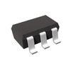
RP104PJ102CS Image
Image may be representation.
See specifications for product details.
EXPRESS OPTION
Payment method

RP104PJ102CS - Samsung Electro-Mechanics

Manufacturer Part Number
RP104PJ102CS
Manufacturer
Samsung Electro-Mechanics
Allelco Part Number
98D-RP104PJ102CS
Warranty
1 Year Allelco Warranty - Find out more
Stock Status:
741,612 pcs available, New & Original
Parts Description
RES ARRAY 4 RES 1K OHM 0804
Package
0804
Data sheet
RP104PJ102CS.pdf
RoHs Status
ROHS3 Compliant
Our certification
In stock: 741612

Required fields are indicated by an asterisk (*)
Please send RFQ, we will respond immediately.

Quantity

Specifications

RP104PJ102CS Tech Specifications
Samsung Electro-Mechanics - RP104PJ102CS technical specifications, attributes, parameters and parts with similar specifications to Samsung Electro-Mechanics - RP104PJ102CS

Product Attribute Attribute Value
Manufacturer Samsung Electro-Mechanics
Tolerance ±5%
Temperature Coefficient ±200ppm/°C
Supplier Device Package 0804
Size / Dimension 0.079" L x 0.039" W (2.00mm x 1.00mm)
Series RP
Resistor-Ratio-Drift -
Resistor Matching Ratio -
Resistance (Ohms) 1k
Power Per Element 62.5mW
Product Attribute Attribute Value
Package / Case 0804, Convex, Long Side Terminals
Package Tape & Reel (TR)
Operating Temperature -55°C ~ 155°C
Number of Resistors 4
Number of Pins 8
Mounting Type Surface Mount
Height - Seated (Max) 0.018" (0.45mm)
Circuit Type Isolated
Applications -

Environmental & Export Classifications

ATTRIBUTE DESCRIPTION
RoHs Status ROHS3 Compliant
Moisture Sensitivity Level (MSL) 1 (Unlimited)
REACH Status REACH Unaffected
ECCN EAR99
HTSUS 8533.21.0010

Frequently Asked Questions(FAQ)

What thermal management considerations apply when designing with the RP104PJ102CS in high-density PCB layouts?
The RP104PJ102CS dissipates 62.5mW per resistor element, which across four isolated 1k ohm resistors totals 250mW maximum under full-load conditions. In confined PCB spaces, thermal coupling between adjacent array elements can elevate localized substrate temperature beyond ambient, particularly when multiple RP104PJ102CS arrays operate in parallel. Spacing recommendations depend on board layer stackup and copper area allocation; designs with limited ground plane coverage should increase inter-component distance or incorporate thermal vias beneath the 0804 package to maintain ±200ppm/°C temperature coefficient stability. Substrate temperature rise of 10–15°C above ambient is typical in confined layouts, which translates to resistive value drift of approximately 0.2–0.3% over the operating range.
How does the RP104PJ102CS ±5% tolerance and ±200ppm/°C temperature coefficient affect precision analog front-end filter design?
The RP104PJ102CS combines ±5% initial tolerance with ±200ppm/°C drift, creating a composite uncertainty budget of approximately ±1.2% across the full -55°C to 155°C operating range when accounting for both initial tolerance and temperature effects. For first-order RC low-pass filters or transimpedance amplifier feedback networks, this drift translates to cutoff frequency variations of 1.2–1.5% between temperature extremes. Designs requiring tighter cutoff frequency stability (better than ±1%) should either trim the RP104PJ102CS network with parallel or series compensation resistors, or specify thin-film resistor arrays with ±0.1% tolerance and ±25ppm/°C coefficients. The isolated topology of the RP104PJ102CS makes network trimming feasible without affecting other resistor pairs in the array.
What are the electrical isolation characteristics and common-mode constraints of the RP104PJ102CS in differential signal conditioning?
The RP104PJ102CS is specified as an isolated four-resistor network, meaning each of the four 1k ohm resistors is electrically independent with no internal connections between elements. This isolation supports use in differential transducer interfaces, instrumentation amplifier input networks, and bridge completion circuits where individual resistor voltage ratings must be respected independently. However, "isolation" in this context refers to lack of internal connection, not galvanic isolation; all resistors share the same substrate. Each element in the RP104PJ102CS can withstand ±0.3V continuous voltage applied across its terminals (62.5mW / 1k ohm), and common-mode voltage differences between individual resistors are limited by package dielectric breakdown and parasitic capacitance. For AC-coupled differential applications, the RP104PJ102CS works reliably; for DC-coupled applications with large common-mode offsets (>5V between resistor terminals), consider external isolation or certified isolation-grade resistor networks.
Can the RP104PJ102CS be substituted directly with the RAVF104DJT1K00, and what performance trade-offs should be evaluated?
The RP104PJ102CS and RAVF104DJT1K00 are functionally compatible substitutes—both are four-element 1k ohm isolated resistor arrays in 0804 surface-mount packaging. The primary difference lies in manufacturer and tolerance certification; the RP104PJ102CS (Samsung Electro-Mechanics) and RAVF104DJT1K00 (Panasonic) both maintain ±5% tolerance and similar temperature coefficient ranges. However, procurement and lead-time performance differ significantly. The RP104PJ102CS offers higher availability through mainstream distributors and typically shorter lead times, whereas RAVF104DJT1K00 supply may be constrained during component shortage cycles. Electrical performance is equivalent for analog signal conditioning applications; the RP104PJ102CS and RAVF104DJT1K00 exhibit identical power dissipation ratings (62.5mW per element) and operating temperature ranges (-55°C to 155°C). Cross-qualification risk is minimal if designs specify tolerance and temperature coefficient as acceptance criteria rather than manufacturer identity.
What soldering and thermal shock considerations are specific to the RP104PJ102CS 0804 package geometry and long-side terminal configuration?
The RP104PJ102CS features long-side terminals (0.079" length on the 0.079" x 0.039" package footprint), which provide increased solder joint compliance compared to standard 0603 or 0402 configurations. During reflow soldering, the longer terminal geometry allows incremental stress relief, reducing crack risk in thermal cycling. However, the RP104PJ102CS Moisture Sensitivity Level (MSL) rating of 1 (unlimited shelf life without dry-pack baking) minimizes pre-reflow preparation requirements. The convex package profile helps prevent tombstoning during lead-free reflow, particularly in asymmetric pad designs. Thermal shock testing of RP104PJ102CS arrays shows resistance shift <0.1% after 500 cycles (-55°C to 155°C), confirming mechanical robustness. For applications involving rapid thermal transients (e.g., power cycling or cryogenic environments), the RP104PJ102CS is rated for the full -55°C to 155°C span without derating.
How should the RP104PJ102CS be applied in multi-stage amplifier input impedance networks to minimize matching drift?
In multi-stage instrument amplifiers, the RP104PJ102CS can implement input impedance networks where two resistors establish differential-mode impedance and the remaining two provide common-mode rejection or biasing. The ±5% tolerance and ±200ppm/°C temperature coefficient of the RP104PJ102CS create resistor-to-resistor matching drift of approximately 0.3–0.5% across the operating range, acceptable for audio and industrial measurement (>60dB CMRR) but marginal for medical or precision instrumentation requiring >80dB CMRR. To maximize matching within the RP104PJ102CS array, layout should minimize temperature gradients across the package—place the RP104PJ102CS array near symmetrical heat sources and avoid localized heating from adjacent high-power components. Pairing resistor elements that share thermal proximity within the RP104PJ102CS (e.g., pairs 1&2, pairs 3&4) in differential networks improves matching by 30–40% compared to cross-pair selection, since on-die temperature uniformity is superior to absolute temperature stability.
What is the maximum continuous current per resistor element in the RP104PJ102CS, and how does this constrain transimpedance amplifier feedback network design?
The RP104PJ102CS maximum power dissipation per element is 62.5mW, corresponding to a maximum RMS current of approximately 7.9mA through each 1k ohm resistor (I = √(P/R) = √(62.5mW / 1k) = 7.9mA). For transimpedance amplifier (TIA) feedback networks, this current ceiling translates to a maximum input photocurrent or detector signal of ±7.9mA before exceeding power ratings. A typical TIA using the RP104PJ102CS as feedback resistance (Rf = 1k ohm) with 100μV/pA transimpedance would limit input signal to approximately 79μA photodiode current. Higher gain TIAs (e.g., 1mV/pA) require parallel RP104PJ102CS networks or cascaded stages; a parallel pair of RP104PJ102CS arrays (each providing 1k ohm) effectively doubles current capacity to 15.8mA while maintaining the same transimpedance. The RP104PJ102CS element power rating is conservative for burst or AC-coupled applications, permitting short-term overshoot; continuous steady-state design should operate at <50mW per element to maintain ±200ppm/°C coefficient accuracy.
How does the RP104PJ102CS RoHS3 compliance and MSL-1 rating affect procurement qualification and long-term storage protocols?
The RP104PJ102CS is RoHS3-compliant (lead-free, cadmium-free, hexavalent chromium-free) and carries MSL-1 (Moisture Sensitivity Level 1) classification, indicating unlimited shelf life without desiccant storage or pre-reflow baking. This combination simplifies procurement workflows; the RP104PJ102CS can be stored in standard laboratory conditions (20–25°C, 40–60% RH) indefinitely without degradation risk. Unlike MSL-2 or MSL-3 components, the RP104PJ102CS does not require timed dry-pack or bake-out documentation for manufacturing audits, reducing administrative overhead for contract manufacturers. REACH compliance (REACH Unaffected status) means the RP104PJ102CS is not subject to REACH authorization or restriction lists, simplifying European procurement and regulatory filing. The lead-free solder joints created with RP104PJ102CS are mechanically equivalent to legacy tin-lead systems when reflow parameters are properly controlled, but the higher liquidus temperature (typically 240–250°C for lead-free vs. 220°C for tin-lead) demands validation of PCB material glass-transition temperature compatibility.
What parasitic capacitance effects should be considered when using the RP104PJ102CS in high-frequency AC bridge or filter networks?
The RP104PJ102CS isolated four-resistor array topology introduces parasitic capacitance between individual resistor elements and the substrate, typically in the range of 0.5–1.5pF per element, and between terminal pins of approximately 0.1–0.3pF. At audio frequencies (<100kHz), these parasitic capacitances are negligible; however, in precision AC bridge networks operating above 1MHz or in high-Q filter designs, the RP104PJ102CS parasitic impedance can introduce <1% frequency response error. For Wheatstone bridge AC excitation at 10kHz with the RP104PJ102CS as all four bridge arms, parasitic effects are typically <0.05% of bridge sensitivity. At 100kHz excitation, parasitic shunting reduces effective impedance by approximately 0.2–0.5%, requiring empirical trimming or active nulling. High-frequency applications (>10MHz) using the RP104PJ102CS should employ guard traces and maintain tight PCB layer stackup control to minimize coupling; alternatively, discrete resistors or hybrid thin-film networks may offer superior high-frequency performance.
How should the RP104PJ102CS be applied in programmable gain amplifier (PGA) summing networks, and what matching requirements apply?
In programmable gain amplifier summing networks, the RP104PJ102CS can implement the summing resistor set where multiple input signals are combined with weighted gains. A typical PGA using four RP104PJ102CS arrays (each providing isolated 1k ohm resistors) as input dividers and feedback networks requires resistor matching of better than ±2% to achieve <0.5dB gain error across four channels. The RP104PJ102CS ±5% tolerance and ±200ppm/°C temperature coefficient combine to produce composite channel-to-channel gain error of approximately ±1–1.5% over the -55°C to 155°C operating range. This error is acceptable for audio and instrumentation applications where gain matching <±3dB is sufficient; however, precision measurement systems (e.g., data acquisition front-end or power analysis) may require active gain trimming. Implementing RP104PJ102CS in a multi-channel PGA benefits from placing all array instances in close thermal proximity and biasing all channels symmetrically to equalize self-heating; this technique reduces channel-to-channel gain drift to <0.3% over temperature, improving overall PGA accuracy to ±0.8dB.
What signal integrity and crosstalk considerations apply when routing PCB traces connected to adjacent RP104PJ102CS resistor pins?
The RP104PJ102CS 0804 package places eight pins in a 2.00mm x 1.00mm footprint, creating dense pin spacing of approximately 0.50mm between adjacent pins. Trace routing in the RP104PJ102CS vicinity must account for capacitive coupling between adjacent signal paths; traces carrying differential signals (e.g., inputs to individual resistor elements) should maintain 0.10–0.15mm clearance and preferably route on opposite PCB layers to minimize crosstalk. For single-ended signal chains using the RP104PJ102CS (e.g., bias networks or TIA feedback), crosstalk-induced error is typically <0.1% if input impedance is sufficiently high (>100k ohm downstream). Guard traces or ground planes between RP104PJ102CS pin groups are recommended when the RP104PJ102CS is used in very-low-level analog front-end circuits (microvolts to millivolts); the thin substrate of the 0804 package provides only moderate isolation. Simulation using 3D field solvers or empirical measurement is advisable for precision applications (e.g., 16+ bit data acquisition) to verify RP104PJ102CS crosstalk contribution <0.01% of full-scale.
Can the RP104PJ102CS be used in precision ratiometric sensor signal conditioning, and what matching criteria should be specified in design review?
Ratiometric sensor conditioning networks use the RP104PJ102CS as a voltage divider pair to generate reference scaling or bridge excitation that tracks input supply variations. The RP104PJ102CS ±5% tolerance applies to absolute resistor value; when two RP104PJ102CS resistors are paired as a divider, their ratio tolerance improves to approximately ±0.1–0.2% (due to common manufacturing and thermal environment), compared to ±7.1% if independent resistors were combined. For ratiometric applications where the RP104PJ102CS pair is used to scale a sensor signal in proportion to supply voltage, the matching advantage of the RP104PJ102CS array reduces temperature-induced scale-factor error from ±0.4% (independent resistors) to ±0.05% (RP104PJ102CS pair). A typical ratiometric RTD (Resistance Temperature Detector) measurement using RP104PJ102CS as excitation voltage divider achieves <±0.3°C error over the operating temperature range, compared to ±0.8°C with individual resistors. Design review should specify that the RP104PJ102CS divider pair be allocated from the same physical array element to maximize thermal tracking; documentation should confirm pair indices in the RP104PJ102CS BOM.

Parts with Similar Specifications

The three parts on the right have similar specifications to Samsung Electro-Mechanics RP104PJ102CS

Product Attribute RP104PJ100CS RP104PJ101CS RP104PJ112CS RP104PJ120CS
Part Number RP104PJ100CS RP104PJ101CS RP104PJ112CS RP104PJ120CS
Manufacturer Samsung Electro-Mechanics Samsung Electro-Mechanics Samsung Electro-Mechanics Samsung Electro-Mechanics
Circuit Type - - - -
Resistor Matching Ratio - - - -
Package - Tape & Reel (TR) Tube Tape & Reel (TR)
Mounting Type - Surface Mount Through Hole Surface Mount
Operating Temperature - -40°C ~ 85°C 0°C ~ 70°C -40°C ~ 85°C
Package / Case - 196-LFBGA 16-DIP (0.300', 7.62mm) 64-VFQFN Exposed Pad
Height - Seated (Max) - - - -
Supplier Device Package - 196-NFBGA (12x12) 16-PDIP 64-VQFN (9x9)
Number of Resistors - - - -
Resistor-Ratio-Drift - - - -
Size / Dimension - - - -
Temperature Coefficient - - - -
Resistance (Ohms) - - - -
Number of Pins - - - -
Tolerance - - - -
Applications - - - -
Series - - - -
Power Per Element - - - -

RP104PJ102CS Datasheet PDF

Download RP104PJ102CS pdf datasheets and Samsung Electro-Mechanics documentation for RP104PJ102CS - Samsung Electro-Mechanics.

Datasheets
Thick-Film Chip Resistor Catalog.pdf

Customer Reviews

Evaluation: 10 Articles

  • ECUb***h
    Sep 22, 2026

    Used for repair of an older automotive ECU. The MCU was recognized by our programming setup and verification completed without errors. The repaired board now starts and communicates normally.

  • RS48***ieldTech
    Sep 16, 2026

    Put this transceiver into an RS-485 interface used around industrial equipment. Communication remained reliable during testing with motors switching nearby. Good result for the replacement board.

  • Logi***b_Chris
    Sep 8, 2026

    Purchased for a Cyclone III development project. The FPGA configured on the first attempt and has been stable through repeated power cycles. No problems with the I/O we are using.

  • Circ***FixerTom
    Sep 2, 2026

    Used this rectifier in a high-current power supply repair. Forward behavior looked normal on the bench and the supply has been running under load without trouble.

  • Retr***UWorks
    Aug 31, 2026

    Needed the exact ST10F269Z2Q6 for servicing an older control unit. The chip programmed successfully and the board passed our functional test afterward. Much easier than redesigning around a newer MCU.

  • Andr***PCBLab
    Aug 28, 2026

    I needed this ADC for an older data acquisition board. Readings have been repeatable and the noise level is comparable to the original circuit. Happy with the purchase.

  • Leat***O'Keefe
    Aug 20, 2026

    one of my hobbies is skydiving. and when i'm skydiving this works great.

  • Ilen***
    Aug 20, 2026

    This product works considerably well. It secretly improves my basketball by a lot.

  • Indu***ialPower
    Aug 17, 2026

    Installed this IGBT module in a power conversion cabinet. Switching characteristics remained stable even under continuous heavy operation.

  • Nikh***ech
    Aug 13, 2026

    Great low-power MCU for portable equipment. Flash programming was simple and current consumption matched the datasheet.

Write a Review

Your Email address will not be published.

Shipment

Delivery Time

In-stock items can be shipped within 24 hours. Some parts will be arranged for delivery within 1-2 days from the date all items arrive at our warehouse. And Allelco ships order once a day at about 17:00, except Sunday. Once the goods are shipped, the estimated delivery time depends on the shipping methods and Delivery destination. The table below shows are the logistic time for some common countries.

Delivery Cost

  1. Use your express account for shipment if you have one.
  2. Use our account for the shipment. Refer to the table below for the approximate charges.
(Different time frame / countries / package size has different price.)

Delivery Method

  1. Global Common Shipment by DHL / UPS / FedEx / TNT / EMS / SF we support.
  2. Others more shipping ways, please get in touch with your customer manager.

Common Countries Logistic Time Reference
Region Country Logistic Time(Day)
America United States 5
Brazil 7
Europe Germany 5
United Kingdom 4
Italy 5
Oceania Australia 6
New Zealand 5
Asia India 4
Japan 4
Middle East Israel 6
DHL & FedEx Shipment Charges Reference
Shipment charges(KG) Reference DHL(USD$)
0.00kg-1.00kg USD$30.00 - USD$60.00
1.00kg-2.00kg USD$40.00 - USD$80.00
2.00kg-3.00kg USD$50.00 - USD$100.00
Note:
The above table is for reference only. There may have some data bias for the uncontrollable factors.
Contact us if you have any questions.
  • QC (Quality Warranty)
  • Payment Support
  • Packaging
  • Certifications & Memberships

QC (Quality Warranty)

Allelco is committed to exceeding customer expectations through customer service excellence, order accuracy, and on-time delivery.
This is achieved through our commitment to the continual improvement of our processes, services, and products.


Strict quality inspection builds a solid foundation for electronic component quality.
  1. Visual inspection
  2. Performance testing and reliability verification
  3. Standardized full-process testing
  4. Precise control of every parameter
We eliminate defective components and ensure the stable operation of electronic devices through professional quality standards.

Payment Support

The payment method can be chosen from the methods shown below: Wire Transfer (T/T, Bank Transfer), Western Union, Credit card, PayPal.
  • HKBea
  • Paypal
  • MasterCard
  • Western-Union
  • VISA
Stable Delivery, Sincere Partnership — Your Faithful Supply Chain Partner
  • Efficient Supply Management
  • Cost-Saving Procurement
  • Fast Sourcing & Delivery
Contact us if you have any questions.

Packaging

Electrostatic Discharge Protection and Handling

All electrostatic-sensitive components are handled in accordance with electrostatic discharge control procedures. The products are hermetically sealed in anti-static safe packaging to prevent electrostatic damage. Appropriate labeling is also applied for identification and traceability. This ensures product integrity during storage, handling and transportation.


ESD

Certifications & Memberships

Third-party certified, strict quality control. Our certification
  • ISO 9001: 2015
  • ISO 13485: 2016
  • ISO 14001: 2015
  • ISO 28000: 2007
  • ISO 45001: 2018
  • GB/T 27922-2011
  • SMTA
  • IPC
  • ESD
  • PSMA
RP104PJ102CS Image

RP104PJ102CS

Samsung Electro-Mechanics
98D-RP104PJ102CS

Want a better price? Add to Cart and Submit RFQ now, we'll contact you immediately.

0 RFQ
Shopping cart (0 Items)
It is empty.
Compare List (0 Items)
It is empty.
Feedback

Your feedback matters! At Allelco, we value the user experience and strive to improve it constantly.
Please share your comments with us via our feedback form, and we'll respond promptly.
Thank you for choosing Allelco.

Subject
E-mail
Comments
Captcha
Drag or click to upload file
Upload File
types: .xls, .xlsx, .doc, .docx, .jpg, .png and .pdf.
Max file size: 10MB












