2N1711 Transistor Guide: Pinout, Specs, and Equivalent Models
The 2N1711 is a silicon-based NPN transistor housed in a durable TO-39 metal package. Known for its reliability, it is a favored choice for designing high-performance amplifiers, oscillators, and switching circuits. With notable specifications like a collector-emitter voltage of 50V and a collector current of up to 3A, the 2N1711 is well-suited for demanding applications. This article digs into the key features, practical applications, and advantages of using the 2N1711, illustrating why it remains a go-to component in precision electronic designs.Catalog

Understanding the 2N1711
The 2N1711 transistor, encased in a TO-39 metal package, plays diverse roles, such as switching, amplification, and oscillation. It handles up to 500mA of collector current in switching and withstands peak collector currents up to 1A, adeptly managing brief surges of high current. This ability makes the 2N1711 a reliable choice for circuits that demand rapid and dynamic responses.
In its practical applications, the flexible nature of the 2N1711 shines. It excels in swiftly switching currents, making it suitable for a range of uses from straightforward signal amplification to intricate oscillation tasks. Its robust design ensures dependable operation in various electronic settings, mirroring lessons learned from actual use where precision and steadiness matter.
The deployment of the 2N1711 emphasizes its requisite role. In audio amplification circuits, for example, it can markedly enhance sound clarity and fidelity. These enhancements show that even with technological advances, traditional components like the 2N1711 remain instrumental in achieving exceptional performance.
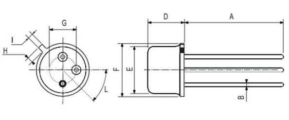
2N1711 Pin Configuration

Technical Specifications
|
Type |
Parameter |
|
Mount |
Through Hole |
|
Mounting Type |
Through Hole |
|
Package / Case |
TO-205AD, TO-39-3 Metal Can |
|
Number of Pins |
3 |
|
Weight |
4.535924g |
|
Transistor Element Material |
Silicon |
|
Collector-Emitter Breakdown Voltage |
50V |
|
Number of Elements |
1 |
|
hFE (Min) |
40 |
|
Operating Temperature |
175°C TJ |
|
Packaging |
Tube |
|
JESD-609 Code |
e3 |
|
Pbfree Code |
Yes |
|
Part Status |
Obsolete |
|
Moisture Sensitivity Level (MSL) |
1 (Unlimited) |
|
Number of Terminations |
3 |
|
Terminal Finish |
Matte Tin (Sn) |
|
Voltage - Rated DC |
75V |
|
Max Power Dissipation |
800mW |
|
Terminal Position |
Bottom |
|
Terminal Form |
Wire |
|
Current Rating |
500mA |
|
Frequency |
100MHz |
|
Base Part Number |
2N17 |
|
Pin Count |
3 |
|
Element Configuration |
Single |
|
Power Dissipation |
800mW |
|
Transistor Application |
Switching |
|
Gain Bandwidth Product |
100MHz |
|
Polarity/Channel Type |
NPN |
|
Transistor Type |
NPN |
|
Collector Emitter Voltage (VCEO) |
50V |
|
Max Collector Current |
500mA |
|
DC Current Gain (hFE) @ Ic, Vce |
35 @ 100mA, 10V |
|
Current - Collector Cutoff (Max) |
10nA ICBO |
|
Vce Saturation (Max) @ Ib, Ic |
1.5V @ 15mA, 150mA |
|
Transition Frequency |
100MHz |
|
Collector Base Voltage (VCBO) |
75V |
|
Emitter Base Voltage (VEBO) |
7V |
|
Height |
6.6mm |
|
Length |
9.4mm |
|
Width |
9.4mm |
|
Radiation Hardening |
No |
|
RoHS Status |
ROHS3 Compliant |
|
Lead Free |
Lead Free |
Features of 2N1711
|
Feature |
Description |
|
Package Type |
TO-39 |
|
Transistor Type |
NPN |
|
Max Collector Current (IC) |
500 mA |
|
Max Collector-Emitter Voltage (VCE) |
50 V |
|
Max Collector-Base Voltage (VCB) |
75 V |
|
Max Emitter-Base Voltage (VBE) |
7 V |
|
Max Collector Dissipation (Pc) |
800 mW |
|
Max Transition Frequency (fT) |
100 MHz |
|
Minimum & Maximum DC Current Gain (hFE) |
100 to 300 |
|
Max Storage, Operating & Junction Temperature Range |
-65°C to 200°C |
Benefits of the 2N1711 Transistor
Enhanced Voltage Management
Known for its resilience in handling elevated voltages, the 2N1711 stands as a guardian against breakdown. In power supply designs, ensuring reliability under stress becomes more apparent. By selecting components with such voltage endurance, electronics endure and thrive in challenging conditions, offering peace of mind to those who rely on them.
Efficient Power Usage
Exhibiting minimal leakage current, the 2N1711 optimizes circuit efficiency by minimizing unwarranted power use during inactivity. Especially in battery-powered devices, this trait becomes a boon, extending intervals between charges and nurturing the life of the device. You can often choose transistors with this feature to craft more sustainable designs.
Signal Precision with Minimal Interference
Due to its low capacitance, this transistor minimizes disruptions in high-frequency signals, becoming a pillar of reliability in RF applications. Where clarity and precision are sought after, such performance ensures communication devices maintain signal integrity, sparking confidence in their users.
Versatile Current Handling for Stable Performance
A wide current range, coupled with the stable beta, offers adaptability in amplification scenarios, gracefully accommodating varying loads without substantial fluctuations in gain. This attribute streamlines design processes, providing consistent performance across different operational landscapes. Transistors with these traits are favored for their reliability in delivering predictable circuit responses.
Applications of 2N1711
Switching Capabilities
The 2N1711 transistor often finds a place in various switching applications. Its solid build makes it suited for handling medium power tasks effortlessly, even in challenging scenarios. You can favor it for circuits needing swift on-off transitions, leveraging its reliable switching proficiency to boost system responsiveness. Experience indicates that its steady performance under diverse conditions makes it a trustworthy choice for dynamic systems.
Audio Amplification
In audio setups, the 2N1711 functions as a competent amplifier. You can appreciate its capability to enhance sound clarity by amplifying signals with minimal distortion. Its role in analog circuits emphasizes its importance in maintaining signal integrity, which is active for high-fidelity audio. You can often turn to it for DIY audio projects, valuing its precision and dependability.
Pre-Amplification
The domain of pre-amplification is another area where the 2N1711 shines. It prepares signals for further amplification stages, ensuring outputs are both clear and faithful. Its low noise profile makes it fitting for sensitive audio and radio frequency applications, where early signal quality plays a major role in the outcome. Using the 2N1711 in pre-amplification can significantly enhance performance.
RF Applications
The reach of the 2N1711 extends to radio frequency tasks, where it handles RF signals effectively. Its capacity to operate at high frequencies makes it valued in RF circuits. You can depend on its stability and precision to sustain consistent communication quality, where maintaining signal strength against interference is active. Actual use of this component often highlights its major role in RF technology advancements.
General Signal Amplification
Beyond specific applications, the 2N1711 is employed for general signal amplification. It assists in projects ranging from small electronics to complex circuit designs, offering useful amplification functions. Its flexibility enables it to meet varying circuit demands with ease, consistently delivering outstanding results across numerous applications. This versatility embodies the broader strategy of using adaptable components to simplify design and execution in diverse technological ventures.
Alternatives to the 2N1711 Transistor
Circuit Functionality of 2N1711

Circuit Details
The 2N1711 transistor showcases remarkable adaptability, fitting seamlessly into common base, common emitter, and common collector configurations. Each setup offers its advantages. The common emitter setup, in particular, is cherished for its impressive voltage and power gain. It often boosts input signal strength by approximately 20dB, translating to a hundredfold increase. Here, the collector voltage surpasses the base voltage, while the emitter current involves both base and collector currents, demonstrating the cumulative current flow.
Doping variations play a key role in transistor operations. The emitter undergoes heavy doping, thereby lowering resistance and enhancing electron injection. Conversely, the collector receives light doping to facilitate efficient collection and minimize power loss. These differences shape amplification traits and ensure reliability across diverse applications.
Comprehending the current amplification factor, indicated by Beta (β), assists in crafting efficient circuits. It defines the ratio of collector current to base current, aiding you in forecasting transistor behavior under varying conditions. Practical applications highlight how careful control of β can significantly sway circuit performance, thus influencing decisions where stability and efficiency are used.
Dimensions
Manufacturer Details
STMicroelectronics emerges as a substantial force in the semiconductor sector, celebrated for its groundbreaking innovations. At the forefront of microelectronics, the company's expertise shines through its cutting-edge capabilities, especially in System-on-Chip (SoC) technologies. Their solutions span a wide array of fields, embedding themselves deeply in the automotive, industrial, personal electronics, and communication sectors, showcasing their far-reaching influence.
The prowess of STMicroelectronics in SoC technology is an initial element of their success, facilitating the merging of intricate functionalities into unified components. By perfecting these solutions, they have profoundly impacted the efficiency and performance of electronic devices. This strategy maximizes space and power efficiency while elevating user experiences across diverse platforms, reflecting their dedication to advancement and excellence.
Datasheet PDF
2N1711 Datasheets:
2N3019 Datasheets:
Frequently Asked Questions [FAQ]
1. What is the use of 2N1711?
The 2N1711 is a silicon-based NPN transistor. It finds its place in high-performance settings such as amplifiers, oscillators, and switches. Its design mostly shines in low-noise amplification, making it a preferred choice for audio and radio frequency uses. In actual applications, it is cherished for enhancing signal clarity in communication devices and sensitive electronics. Studying successful implementations highlights how component selection influences overall system performance.
2. How does 2n1711 work?
The 2N1711 operates as a bipolar junction transistor (BJT), using both holes and electrons for conduction. By applying a positive voltage to the base, the transistor modulates larger currents between the emitter and collector, functioning as a current amplifier. This process allows for precise control in electronic circuits, showcasing its role in regulation and signal modulation. Insights from the industry show that skillful manipulation of base current can significantly enhance the transistor's performance, illustrating the intricacies of strategic electronics engineering.
About us
ALLELCO LIMITED
Read more
Quick inquiry
Please send an inquiry, we will respond immediately.
BTA16-600B Triacs Explained: Pinout, Circuit Diagrams, and Datasheet
on October 24th

IRLML2502 MOSFET: Features, Applications, and Specifications
on October 24th
Popular Posts
-

Complex Instruction Set Computers: How They Changed Computing?
on April 18th 147749
-

USB-C Pinout and Features
on April 18th 111901
-

Using Xilinx Unified Simulation Primitives: A Comprehensive Guide to FPGA Design and Simulation
on April 18th 111349
-

Power Supply Voltages in Electronics: Meaning of VCC, VDD, VEE, VSS, and GND
on April 18th 83714
-

RJ45 Connector Guide: Pinout, Wiring, Cable Types, and Uses
on January 1th 79502
-

The Ultimate Guide to Wire Color Codes in Modern Electrical Systems
The way our electrical systems use colors isn’t just for looks. Each wire color now indicates a specific function, making it easier to identify and handle electrical components correctly during ins...on January 1th 66866
-

Quality (Q) Factor: Equations and Applications
The quality factor, or 'Q', is important when checking how well inductors and resonators work in electronic systems that use radio frequencies (RF). 'Q' measures how well a circuit minimizes energy...on January 1th 63004
-

Purge Valve Guide: Function, Symptoms, Testing, and Replacement for Optimal Engine Performance
The purge valve is a key part of a car’s system that helps keep the air clean by managing fuel vapors before they can escape into the atmosphere. This not only helps the environment by reducing pol...on January 1th 62934
-

Achieving Peak Performance with the Maximum Power Transfer Theorem
The Maximum Power Transfer Theorem explains how energy from a source, such as a battery or generator, flows to a connected load. It shows the exact condition where the load receives the most power....on January 1th 54074
-

A23 Battery Specifications and Compatibility
The A23 battery is a small, cylinder-shaped battery with high voltage. Also called 23A, 23AE, or MN21, it runs at 12 volts and much higher than AA or AAA batteries. Its special design make...on January 1th 52087
HOT Part Number
-

XC3S50A-4VQG100C
AMD
IC FPGA 68 I/O 100VQFP
SI1102-A-GM
Silicon Labs
SENSOR OPT REFLECTIVE 50CM 8WDFN
TCN4-13+
Mini-Circuits
1:4 LTCC TRANSFORMER, 650 - 1250
VF30100S-E3/4W
Vishay General Semiconductor - Diodes Division
DIODE SCHOTTKY 100V 30A ITO220AB
GRM033R70J103KA01D
Murata Electronics
CAP CER 10000PF 6.3V X7R 0201
QMK212B7102MDHT
Taiyo Yuden
CAP CER 1000PF 250V X7R 0805
M82351G-12
MACOM Technology Solutions
ACCESS VOICE PROCESSOR
74LV132D,112
Nexperia USA Inc.
IC GATE NAND SCHMIT 4CH 2IN 14SO
AH1801-FJG-7
Diodes Incorporated
MAG SWITCH OMNIPOLAR DFN2020B-3
DG412DY-T1-E3
Vishay Siliconix
IC SWITCH SPST-NOX4 35OHM 16SOIC
PIC16F876A-I/SO
Microchip Technology
IC MCU 8BIT 14KB FLASH 28SOIC
LXA08FP600
Power Integrations
DIODE GP 600V 8A TO220 FULL PACK
FM25V20A-DG
Infineon Technologies
IC FRAM 2MBIT SPI 40MHZ 8DFN
CY7C1011CV33-10ZXC
Cypress Semiconductor Corp
IC SRAM 2MBIT PARALLEL 32TSOP II
04023C221KAT2A
KYOCERA AVX
CAP CER 220PF 25V X7R 0402
RO3101A
Murata Electronics
SAW RES 433.9200MHZ SMD
XRD9818ACGTR
MaxLinear, Inc.
IC AFE 3 CHAN 16BIT 28TSSOP
CL21F104ZBANNNC
Samsung Electro-Mechanics
CAP CER 0.1UF 50V Y5V 0805 -

BZT52-B16_R1_00001
Panjit International Inc.
SOD-123, ZENER
P0300ECL
Littelfuse Inc.
THYRISTOR 25V 400A TO226-2
TPS73615DBVTG4
Texas Instruments
IC REG LINEAR 1.5V 400MA SOT23-5
SN74AXC4T774BQBR
Texas Instruments
IC TRANSCEIVER HALF 4/4 16WQFN
170M5954
Eaton - Bussmann Electrical Division
FUSE SQUARE 350A 1KVAC RECT
CC0805KRX7R9BB682
YAGEO
CAP CER 6800PF 50V X7R 0805
SRP7028A-6R8M
Bourns Inc.
FIXED IND 6.8UH 4.5A 60 MOHM SMD
SMAJ150CA
Taiwan Semiconductor Corporation
TVS DIODE 150VWM 243VC DO214AC
PE-68675
Pulse Electronics
IC CHIP
MAX14890EATJ+
Analog Devices Inc./Maxim Integrated
IC RECEIVER 0/4 32TQFN
TFZGTR20B
Rohm Semiconductor
DIODE ZENER 20V 500MW TUMD2
1N5406-E3/73
Vishay General Semiconductor - Diodes Division
DIODE GEN PURP 600V 3A DO201AD
ME501610
Powerex Inc.
BRIDGE RECT 3P 1.6KV 100A MODULE
GRM1555C2A5R8DA01D
Murata Electronics
CAP CER 5.8PF 100V C0G/NP0 0402
MRF8S19140HSR3
NXP USA Inc.
FET RF 65V 1.96GHZ NI780HS
TN2130K1-G
Microchip Technology
MOSFET N-CH 300V 85MA TO236AB
ADL5519ACPZ-R7
Analog Devices Inc.
IC AMP LOG DETECT CTRLR 32LFCSP
SP3222ECT-L
MaxLinear, Inc.
IC TRANSCEIVER FULL 2/2 18SOIC -
502AT-2
Semitec USA Corp
NTC THERMISTORS 5KOHM 1%
NFM18CC101R1C3D
Murata Electronics
CAP FEEDTHRU 100PF 20% 16V 0603
PS2562L-1-F3-A
Renesas Electronics America Inc
OPTOISOLATOR 5KV DARL 4SMD
502494-0370
Affinity Medical Technologies - a Molex company
2.0 W/B SGL R/ARECASSY3CKTEMBSTP
C1206C223K5RACTU
KEMET
CAP CER 0.022UF 50V X7R 1206
NIS5102QP2HT1G
onsemi
IC HOT SWAP CTRLR GP 12PLLP
VI-J62-MY
Vicor Corporation
DC DC CONVERTER 15V 50W
ADR441ARMZ-REEL7
Analog Devices Inc.
IC VREF SERIES 0.12% 8MSOP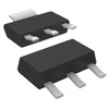
MIC5200-5.0BS
Microchip Technology
IC REG LINEAR 5V 100MA SOT223-3
TAS3251DKQR
Texas Instruments
IC AMP D MONO/STER 350W 56HSSOP
GRM1886T1H360JD01D
Murata Electronics
CAP CER 36PF 50V T2H 0603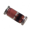
TZM5249B-GS08
Vishay General Semiconductor - Diodes Division
DIODE ZENER 19V 500MW SOD80
LM2575-5.0YWM
Microchip Technology
IC REG BUCK 5V 1A 24SOIC
RT0402BRE075K6L
YAGEO
RES SMD 5.6K OHM 0.1% 1/16W 0402
C0603JB1A104M030BC
TDK Corporation
CAP CER 0.1UF 10V JB 0201
CSD17571Q2
Texas Instruments
MOSFET N-CH 30V 22A 6SON
P4SMA13CA
Bourns Inc.
TVS DIODE 11.1VWM 18.2VC DO214AC
AR0144ATSM20XUEA0-DPBR
onsemi
1MP 1/4 CIS SO