74LS08 AND Two Input Gate IC: Pinout and Specifications
The 74LS08 Integrated Circuit (IC), a prominent member of the 74XX series, stands out for its quadruple 2-input AND gates, each powered by Schottky transistors for high-speed digital applications. This article explores the 74LS08's specifications, pin configurations, and practical uses, highlighting its role in enhancing system efficiency and reliability in diverse technological environments. Through a comprehensive analysis, this article aims to provide valuable insights into optimizing digital systems using the versatile and robust 74LS08 IC.Catalog

What is the 74LS08?
The 74LS08 integrated circuit encompasses four separate AND gates, each with two inputs, leveraging Schottky transistors to facilitate fast logic operations. Many frequently choose the 74LS08 for digital systems, where quick response and efficiency drive innovation. Its design supports logic functions in computing and communications, allowing to optimize performance across a spectrum of circuit complexities. Integrating the 74LS08 requires nuanced planning. You must ensure it meshes well with other components, considering elements such as signal integrity and power efficiency. Challenges often illuminate these aspects, with adept fine-tuning their approaches to address them effectively. The 74LS08 enriches logic processing with its speed and dependable functionality. Its thoughtful integration can uplift circuit capabilities, embodying in technological design. Insights from related models further enhance results, showcasing the interconnectedness of these technologies.
74LS08 Equivalents
• 74LS73
• 74LS00
• 74LS02
• 74LS04
• 74LS138
• SN54LS08
• IC 7408
• HEF4081
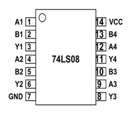
74LS08 Pin Configuration
|
Pin Number |
Description |
|
AND GATE 1 |
|
|
1 |
A1-INPUT1 of GATE 1 |
|
2 |
B1-INPUT2 of GATE 1 |
|
3 |
Y1-OUTPUT of GATE1 |
|
AND GATE 2 |
|
|
4 |
A2-INPUT1 of GATE 2 |
|
5 |
B2-INPUT2 of GATE 2 |
|
6 |
Y2-OUTPUT of GATE2 |
|
AND GATE 3 |
|
|
9 |
A3-INPUT1 of GATE 3 |
|
10 |
B3-INPUT2 of GATE 3 |
|
8 |
Y3-OUTPUT of GATE3 |
|
AND GATE 4 |
|
|
12 |
A4-INPUT1 of GATE 4 |
|
13 |
B4-INPUT2 of GATE 4 |
|
11 |
Y4-OUTPUT of GATE4 |
|
SHARED TERMINALS |
|
|
7 |
GND- connected to ground |
|
14 |
VCC-Connected to a positive voltage to provide power to
all four gates |
74LS08 Symbol and Footprint


Specifications of 74LS08
Technical specifications, attributes, and parameters of the SIGNETICS CORP 74LS08, including parts with comparable specifications to the 74LS08N.
|
Type |
Parameter |
|
Surface Mount |
NO |
|
HTS Code |
8542.39.00.01 |
|
Terminal Form |
THROUGH-HOLE |
|
Supply Voltage |
5V |
|
Qualification Status |
Not Qualified |
|
Supply Voltage-Max (VSUp) |
5.25V |
|
Supply Voltage-Min (VSUp) |
4.75V |
|
Number of Inputs |
2 |
|
Propagation Delay (tpd) |
20 ns |
|
Number of Terminals |
14 |
|
Terminal Position |
DUAL |
|
Number of Functions |
4 |
|
JESD-30 Code |
R-PDIP-T14 |
|
Operating Temperature (Max) |
70°C |
|
Temperature Grade |
COMMERCIAL |
|
Family |
LS |
|
Logic IC Type |
AND GATE |
Features of 74LS08
Energy Efficiency and Power Source
The 74LS08 operates seamlessly on a 5V supply, drawing minimal power. This trait enhances its appeal for battery-operated designs, where energy conservation is key to prolonging device life. Additionally, the limited power draw aids in maintaining lower temperatures, beneficial in compact circuit arrangements.
Output Current Performance
Each gate can deliver up to 8mA, adequately powering various TTL logic circuits. This current capacity ensures compatibility with diverse digital components. In system design, it’s good to manage each gate within this current threshold to avoid unnecessary wear and safeguard the IC's durability.
Timing Attributes
Presenting rise and fall times around 18ns, the 74LS08 suits applications needing moderate speed. These timing features cater to digital projects where swift reaction times are needed without taxing high-speed capacities. This balance garners appreciation, as it affords stable functionality without overburdening other parts.
Storage Temperature Range
The IC is robust enough to withstand storage temperatures from -65°C to 150°C. This extensive range signifies the 74LS08's resilience during storage and transit in varied environments, reducing risk of damage. It benefits manufacturers and distributors engaged in global logistics, easing storage challenges across different climates.
Applications of 74LS08
Digital Electronics
The 74LS08 finds itself at the heart of digital circuit design, often serving as a component in intricate logic systems. Its consistent reliability and speed make it well-suited for applications like timing circuits, flip-flops, and various logic gate configurations. This dependable performance in practical scenarios enhances the efficiency of circuit design and execution.
Server Systems
In server environments, the 74LS08 plays a role in directing data flow and managing control signals. Its proficiency in executing AND logic operations facilitates seamless processing and communication among components, highlighting its role in sustaining operational integrity and system resilience during heavy loads.
Memory Management
Within memory architectures, the 74LS08 is tasked with controlling access to ensure data consistency. Its robust logic capabilities manage read/write operations, forming a stable base for memory addressing and data validation. These applications demonstrate its role in improving data integrity and system efficacy.
Arithmetic Logic Units (ALUs)
In the realm of ALUs, the 74LS08 assists in executing mathematical operations and data manipulation. With fast switching capabilities, it enables swift logic operations, contributing to effective arithmetic processing. These features exemplify its contribution to optimizing computational tasks and boosting processing speed.
General AND Logic Operations
The 74LS08 is frequently utilized for straightforward AND logic tasks across various electronic circuits. Its Schottky design minimizes switching delays, making it suitable for high-speed applications requiring rapid logic processing. This versatility show its adaptability across diverse electronic applications.
The extensive applications of the 74LS08 IC highlight its versatility in modern technology. By seamlessly integrating into various systems, it facilitates efficient and reliable operations across multiple sectors. Its enduring performance in diverse settings reflects a profound understanding of electronic design principles.
Capabilities of the 74LS08 AND Gate

The 74LS08 IC plays a role in digital logic systems, excelling in executing AND operations. With an ability to power multiple gates at once, it's highly valued in settings where quick response and trustworthiness resonate deeply. Employing Schottky transistor technology, the 74LS08 shines in delivering swift processing, which is a core of modern digital circuitry. Schottky transistors bring an enhancement by cutting down propagation delay. Systems demanding rapid operations thrive on this design, as it deftly reduces the latency typical of traditional logic gates. This swift response appeals to applications spanning computational tasks to data processing.
The 74LS08 finds extensive use in computing and automation sectors. It's prominently featured in data routers and signal processing units, a testament to its robust character. Many opt for this IC when crafting circuits that thrive on steady performance, ensuring efficiency even when tackling demanding workloads. The seamless integration of the 74LS08 into intricate circuits highlights its versatility. Modular systems gain substantially as the IC supports expansion without draining excessive power. This adaptability fosters innovative circuit solutions, allowing alterations to design specifications effortlessly, without needing to replace existing components.
A well-thought-out approach to utilizing the 74LS08 involves factoring in thermal management strategies. Given the heat dissipation tied to high-speed operations, introducing suitable cooling mechanisms for upholding long-term reliability. Such foresight in design enhances performance and extends the life of the system, aligning with circuit wisdom. The 74LS08 AND Gate distinguishes itself in digital logic design with its speed and adaptability. Grasping its capabilities enhances its application, making it a preferred choice in numerous advanced technological settings.
Dimensions of 74LS08

74LS08 Manufacturer Information
Founded in 1961, the company began as Signetics, a trailblazer in the integrated circuit revolution, driven by an unwavering pursuit of innovation. This bold approach sparked their acquisition by Philips, marking a phase of dynamic growth. Integrating into Philips expanded their technological reach and fortified their standing as pioneers in electronic advancements, allowing them to explore new horizons. The company's contributions highlight the vibrant evolution of the electronics field. Their innovative strides have extensive effects across multiple sectors, indicating a future of technology interwoven with their advancements. By fostering a culture of continuous enhancement, they not only adapt but actively mold the changing electronics landscape. This enduring commitment to progress acts as a catalyst for profound industry shifts. The transformation from Signetics to their current form under NXP represents an extraordinary odyssey of creativity and resilience.
Frequently Asked Questions [FAQ]
1. What does the 74LS08 primarily do?
The 74LS08 operates as a digital AND logic gate processor, working with two input states: HIGH (3-5V) and LOW (0-2.6V). It plays a role in performing logical conjunctions within digital circuits, smoothly conducting logical operations in computational tasks. Its steadfast presence in digital electronics showcases a deep-seated reliability in situations requiring precise logical outcomes.
2. How many gates does the 74LS08 contain?
The chip features four 2-input AND gates, powered by a single supply, crafted to handle diverse functionalities. This structure ensures seamless adaptability to various circuit needs, simplifying designs and reducing power usage. The inclusion of multiple gates within one chip reflects a thoughtful strategy to streamline circuit creation while avoiding integration hurdles.
3. What are the distinctions between the 74LS00 and the 7400?
The 74LS00 series offers enhanced speed and refined efficiency, though it delivers a lower current output compared to the 7400 series. This difference plays a role in scenarios where power conservation and performance boost. The subtle yet meaningful variations between these series highlight the thoughtful considerations in choosing suitable logic components for distinct purposes.
4. How do the 74LS08 and 74HC08 differ?
The 74LS08 uses TTL logic with a stable 5V supply, while the 74HC08 utilizes CMOS technology, accommodating a voltage range of 2V to 6V. This difference in technology caters to a wider array of applications and power conditions. The flexibility of CMOS technology in the 74HC08 emphasizes its usefulness in situations requiring operational versatility without sacrificing performance efficiency.
About us
ALLELCO LIMITED
Read more
Quick inquiry
Please send an inquiry, we will respond immediately.

LM3524: Pinout, Specifications, and Datasheet
on October 24th

A Comprehensive Guide to the 74LS04
on October 24th
Popular Posts
-

Complex Instruction Set Computers: How They Changed Computing?
on April 18th 147749
-

USB-C Pinout and Features
on April 18th 111920
-

Using Xilinx Unified Simulation Primitives: A Comprehensive Guide to FPGA Design and Simulation
on April 18th 111349
-

Power Supply Voltages in Electronics: Meaning of VCC, VDD, VEE, VSS, and GND
on April 18th 83714
-

RJ45 Connector Guide: Pinout, Wiring, Cable Types, and Uses
on January 1th 79502
-

The Ultimate Guide to Wire Color Codes in Modern Electrical Systems
The way our electrical systems use colors isn’t just for looks. Each wire color now indicates a specific function, making it easier to identify and handle electrical components correctly during ins...on January 1th 66872
-

Quality (Q) Factor: Equations and Applications
The quality factor, or 'Q', is important when checking how well inductors and resonators work in electronic systems that use radio frequencies (RF). 'Q' measures how well a circuit minimizes energy...on January 1th 63005
-

Purge Valve Guide: Function, Symptoms, Testing, and Replacement for Optimal Engine Performance
The purge valve is a key part of a car’s system that helps keep the air clean by managing fuel vapors before they can escape into the atmosphere. This not only helps the environment by reducing pol...on January 1th 62951
-

Achieving Peak Performance with the Maximum Power Transfer Theorem
The Maximum Power Transfer Theorem explains how energy from a source, such as a battery or generator, flows to a connected load. It shows the exact condition where the load receives the most power....on January 1th 54078
-

A23 Battery Specifications and Compatibility
The A23 battery is a small, cylinder-shaped battery with high voltage. Also called 23A, 23AE, or MN21, it runs at 12 volts and much higher than AA or AAA batteries. Its special design make...on January 1th 52092
HOT Part Number
-

BD9B100MUV-E2
Rohm Semiconductor
IC REG BUCK ADJ 1A 16VQFN
UPD70F3539AF5A9-PN7-Q-A
Renesas Electronics America Inc
IC MICROCONTROLLER
18081A621JAT2A
KYOCERA AVX
CAP CER 620PF 100V NP0 1808
FDN340P
onsemi
MOSFET P-CH 20V 2A SUPERSOT3
70231-101
Amphenol ICC (FCI)
CONN RCPT BLADE PWR 8POS EDGE MT
MPSW42RLRAG
onsemi
TRANS NPN 300V 0.5A TO92
MC7824BT
onsemi
IC REG LINEAR 24V 1A TO220AB
AD8009ARZ-REEL
Analog Devices Inc.
IC OPAMP CFA 1 CIRCUIT 8SOIC
LT1815CS5#TRPBF
Analog Devices Inc.
IC OPAMP VFB 1 CIRCUIT TSOT23-5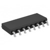
DG411DYZ
Renesas Electronics America Inc
IC SWITCH SPST-NCX4 35OHM 16SOIC
VFT2060C-M3/4W
Vishay General Semiconductor - Diodes Division
DIODE SCHOTTKY 20A 60V ITO-220AB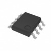
TSX562AIYST
STMicroelectronics
IC CMOS 2 CIRCUIT 8MINISO
MR256D08BMA45
Everspin Technologies Inc.
IC RAM 256KBIT PARALLEL 48FBGA
VSC3312YYP-01
Microchip Technology
IC SWITCH 16X16 6.5GBPS 196FCBGA
XC68HC908GP20CFB
Motorola
TSG 8BIT20K FLASH
CSR8811A08-ICXR-R
Qualcomm
IC RF TXRX+MCU BLUETOOTH
MPSW05
onsemi
TRANS NPN 60V 0.5A TO92
1N4055R
Solid State Inc.
DIODE GEN PURP REV 900V 275A DO9 -

ASX342ATSC00XPED0-DP
onsemi
IMAGE SENSOR VGA 1/4 CIS SOC
0433.125NR
Littelfuse Inc.
FUSE BOARD MNT 125MA 125VAC/VDC
1SMA5941BT3G
onsemi
DIODE ZENER 47V 1.5W SMA
DCP010512BP-U/700
Texas Instruments
DC DC CONVERTER 12V 1W
1-1734344-1
TE Connectivity AMP Connectors
CONN D-SUB HD RCPT 15P R/A SLDR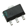
KSD1621STF
onsemi
TRANS NPN 25V 2A SOT89-3
BQ24161RGET
Texas Instruments
IC BATT CHG LI-ION 1CELL 24VQFN
BTA26-600BW
STMicroelectronics
TRIAC ALTERNISTOR 600V 25A TOP3
NCP1239DD65R2G
onsemi
IC OFFLINE SWITCH FLYBACK 7SOIC
TMS320TCI6482BZTZA
Texas Instruments
TMS320 - DIGITAL SIGNAL PROCESSO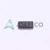
BQ20Z90DBTR-V150
Texas Instruments
IC GAS GAUGE LI-ION 30TSSOP
PCMB104T-1R0MT
Susumu
FIXED IND 1UH 18A 3.3 MOHM SMD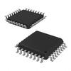
CY29942AXCT
Infineon Technologies
IC CLK BUFFER 1:18 200MHZ 32TQFP
CC0402KRX7R9BB561
YAGEO
CAP CER 560PF 50V X7R 0402
STPS20M60SG-TR
STMicroelectronics
DIODE SCHOTTKY 60V 20A D2PAK
AT25010N-10SC-2.7
Microchip Technology
IC EEPROM 1KBIT SPI 3MHZ 8SOIC
04023A1R0CAT4A
KYOCERA AVX
CAP CER 1PF 25V C0G/NP0 0402
ISL6327IRZ
Intersil
SWITCHING CONTROLLER, VOLTAGE-MO -

LQW18AN75NG0ZD
Murata Electronics
FIXED IND
DFA100BA160
SanRex Corporation
DIODE MODULE 1600V 100A
BAR46AFILM
STMicroelectronics
DIODE ARRAY SCHOTTKY 100V SOT23
MAX825SEUK
Analog Devices Inc./Maxim Integrated
IC SUPERVISOR MPU
MMST2222A-7-F
Diodes Incorporated
TRANS NPN 40V 0.6A SOT323
FODM8801AR2
onsemi
OPTOISO 3.75KV TRANS 4-MINI-FLAT
FJV1845FMTF
Fairchild Semiconductor
SMALL SIGNAL BIPOLAR TRANSISTOR,
EVK105RH5R1JW-F
Taiyo Yuden
CAP CER 5.1PF 16V R2H 0402
6651170-3
TE Connectivity AMP Connectors
CONN EDGE DUAL FMALE 4POS 0.508
KSZ8893FQLI-FX
Microchip Technology
IC SWITCH ETH 3PORT 128QFP
170M6340
Eaton - Bussmann Electrical Division
FUSE SQUARE 400A 1.3KVAC RECT
BCM20741A2KFB1G
Broadcom Limited
SINGLE-CHIP BLUETOOTH
MAX3443EASA+
Analog Devices Inc./Maxim Integrated
IC TRANSCEIVER HALF 1/1 8SOIC
GRM0335C1H9R3DA01D
Murata Electronics
CAP CER 9.3PF 50V C0G/NP0 0201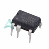
TNY175PN
Power Integrations
11.5 W (85-265 VAC) 15 W (230 VA
742700726
Würth Elektronik
FERRITE CORE 278 OHM SOLID 4MM
DM74S20N
onsemi
IC GATE NAND 2CH 4-INP 14DIP
P4SMA56CA-E3/61
Vishay General Semiconductor - Diodes Division
TVS DIODE 47.8VWM 77VC DO214AC