A Guide to the ADS1115: Compact and Low-Power 16-Bit ADC
The ADS1115 IC by Texas Instruments redefines precision and adaptability in the world of analog-to-digital conversion. With its high-resolution 16-bit ADC, programmable gain amplifier (PGA), and advanced comparator functionality, this compact device surpasses the limitations of built-in ADCs in microcontrollers like Arduino and ESP8266. Ideal for applications requiring exceptional accuracy, such as environmental monitoring, biomedical devices, and battery management, the ADS1115 seamlessly bridges the gap between analog signals and digital processing. In this article, we’ll explore the pin configuration, features, working principles, and versatile applications of the ADS1115, shedding light on how it elevates data acquisition systems and simplifies project designs. Dive in to discover how this versatile ADC enhances precision and reliability across a wide spectrum of industries.Catalog

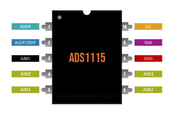
Pinout Configuration
|
Pin Name |
Pin Description |
|
ADDR |
I2C address select (slave) |
|
ALERT/RDY |
Digital comparator output or conversion ready |
|
GND |
Ground |
|
AIN0 |
Differential channel 1: Single-ended channel 1 input or
Negative input |
|
AIN1 |
Differential channel 1: Single-ended channel 2 input or
Negative input |
|
AIN2 |
Differential channel 2: Single-ended channel 3 input or
Positive input |
|
AIN3 |
Differential channel 2: Single-ended channel 4 input or
Negative input |
|
VDD |
Power supply: 2.0V to 5.5V |
|
SDA |
Serial data: Transmits and receives data (used for I2C
communication) |
|
SCL |
Serial clock input: Clocks data on SDA (used for I2C
communication) |
Features & Specs
|
Feature |
Specification |
|
Operating Temperature Range |
–40°C to +125°C |
|
Supply Range |
2.0 V to 5.5 V (Minimum AVDD: 2V, Maximum Input Voltage:
5.5V) |
|
Low Current Consumption |
150 μA (in Continuous-Conversion mode) |
|
Interface |
I2C (Four pin-selectable addresses) |
|
Comparator |
Programmable |
|
Inputs |
Four single-ended inputs or two differential inputs |
|
Settling Time |
Single-Cycle |
|
Data Rate |
Programmable, 8 SPS to 860 SPS |
|
Oscillator |
Internal |
Equivalent Models
When considering alternatives within the same product family, several options present themselves:
• ADS1113
• ADS1114
• ADS1013
• ADS1014
• ADS1015
In the world of analog-to-digital conversion, a few notable ICs stand out:
• ADC0804: This device comes in a DIP-20 package and offers 8-bit resolution for analog-to-digital conversion.
• ADC0808: Packaged in DIP-28, this 8-bit A/D converter features an 8-channel multiplexer, enhancing its versatility.
• ADC0809: Similar to the ADC0808, this device is also an 8-bit A/D converter with an 8-channel multiplexer, presented in a DIP-28 package.
Additionally, the landscape of ADCs includes a variety of other noteworthy options:
• HI7190IP
• MC1408
• ICL7135
• MAX186
• MCP3201
• MCP3008
• MCP3202
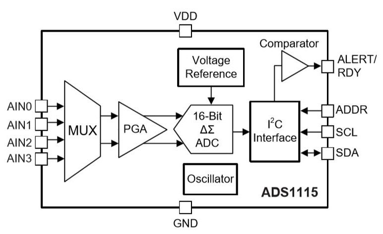
Working Principle of the ADS1115 IC
The ADS1115 operates by processing four analog inputs (A0, A1, A2, A3), which are routed through a multiplexer to the Programmable Gain Amplifier (PGA). This architecture allows the Analog-to-Digital Converter (ADC) to handle a wide input range, spanning from ±256 mV to ±6.144 V. Once the signal is amplified, it undergoes conversion into a 16-bit digital format, which is subsequently transmitted via the I2C interface utilizing the SDA, SCL, and ADDR pins.
Multiplexing and Signal Amplification
The multiplexer is basic to the operation of the ADS1115, as it decides which analog input is being processed at any given moment. By sequentially selecting each input, the ADS1115 efficiently manages multiple signals without the need for extra components. This feature is mainly advantageous in scenarios where both space and budget are limited. Additionally, the Programmable Gain Amplifier enhances the flexibility of the ADS1115, enabling you to customize gain settings based on the unique attributes of the input signals. Such adaptability fosters accuracy in applications with fluctuating signal levels, ensuring that the ADC remains within its optimal operational range.
Conversion Process and Digital Output
The ADS1115's conversion process is meticulously designed to achieve high precision. With a 16-bit resolution, it can represent 65,536 discrete values, allowing for subtle distinctions between input levels. This granularity is mainly remarkable in sensor data acquisition, where even minor variations in the input signal can hold substantial importance. The digital output, communicated through the I2C interface, simplifies integration with microcontrollers and other digital devices. The I2C protocol, recognized for its straightforwardness and efficiency, permits multiple devices to share the same communication lines, thereby enhancing the overall system architecture.
Comparator Functionality
A noteworthy aspect of the ADS1115 is its built-in programmable digital comparator, which continuously evaluates the analog input against a predefined reference voltage. This capability can activate output signals for ready (RDY) or alert states, facilitating prompt responses to fluctuations in the input signal. Such functionality is used in actual monitoring systems, where swift actions are required based on sensor readings. For example, in environmental monitoring applications, the comparator can notify a microcontroller when pollutant levels surpass safe thresholds, enabling timely interventions to safeguard health and safety.
Utilizing the ADS1115 Analog to Digital Converter IC
The ADS1115, presented on an accessible breakout board, offers a seamless integration experience with various platforms, including Arduino, ESP8266, and Raspberry Pi, through its I2C interface. This 16-bit precision ADC features four multiplexed inputs, enabling both individual and differential measurements. Such adaptability fosters a sense of reliability, especially when leveraging its calibrated reference for enhanced accuracy.
The ADS1115 operates by transforming analog signals into digital data, which microcontrollers can readily process. This conversion plays a notable role in applications that demand precise measurements, such as environmental monitoring and data acquisition systems. You can choose between single-ended and differential inputs, tailoring the device to meet specific measurement requirements. For example, utilizing differential measurements can significantly minimize noise, a notable advantage in environments with electrical interference.
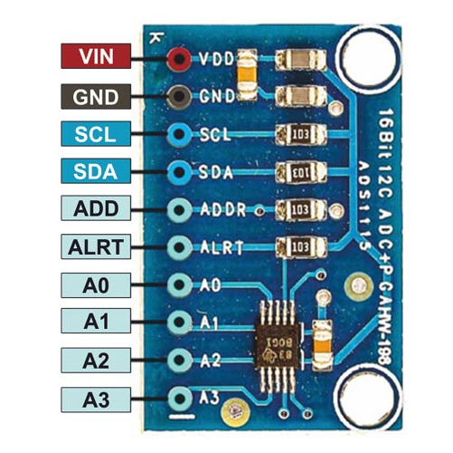
To facilitate connections, the required wiring between the ADS1115 Breakout Board and an Arduino is outlined in the table below:
|
Arduino Board Pin |
ADS1115 Pin |
Description |
|
5V |
VDD |
Power supply to ADS1115 |
|
GND |
GND |
Ground connection |
|
A5 |
SCL |
I2C Clock line |
|
A4 |
SDA |
I2C Data line |
|
GND |
ADDR |
Sets the I2C address |
|
2 |
ALRT |
Alert/Ready pin for interrupt |
|
Wiper of 10k pot. |
A1 |
Analog input channel A1 |
Connect the ends of the 10k potentiometer to 5V and GND. Additionally, connect a 100nF capacitor between 5V and GND.

Uses
The ADS1115 has established a prominent presence across a wide spectrum of applications, emphasizing its adaptability and high performance. Its integration into consumer electronics not only enhances your experience but also resonates with the desire for precision in data acquisition. For example, in portable instrumentation, the ADS1115 facilitates accurate readings that are dynamic for field measurements, thereby fostering a sense of trust and reliability in varied environments.
Consumer Electronics
Within the consumer electronics sector, the ADS1115 is frequently utilized in devices demanding high-resolution analog-to-digital conversion. This encompasses audio equipment, where sound quality is of utmost importance. The device's capability to detect subtle variations in signal can significantly elevate audio fidelity, a factor that resonates deeply with you. You can often express their satisfaction, noting that systems equipped with the ADS1115 deliver a clarity and depth of sound that profoundly enhances their listening experience.
Portable Instrumentation
The significance of the ADS1115 in portable instrumentation is noteworthy. Its low power consumption renders it ideal for battery-operated devices, where efficiency holds considerable value. For instance, in environmental monitoring tools, the ADS1115 provides precise readings of temperature and humidity, which are used for research and data collection. You can frequently remark that the dependability of data from these instruments substantially affects the integrity of their findings, highlighting the emotional investment in accurate research outcomes.
Temperature Measurement Systems
Temperature measurement systems gain substantial advantages from the precision offered by the ADS1115. In applications spanning industrial processes to home automation, maintaining accurate temperature readings is a must. The incorporation of the ADS1115 enables present monitoring, which can prompt timely interventions in process control. Observations indicate that systems employing this component experience fewer fluctuations, fostering a stable operational environment that contributes to peace of mind for you.
Battery Voltage and Current Monitoring
The ADS1115 proves to be mostly beneficial in applications focused on battery voltage and current monitoring. Its ability to deliver precise measurements aids in optimizing battery performance and extending longevity. You can note that battery management systems incorporating the ADS1115 allow for effective tracking of charge levels and discharge rates. This capability enhances decision-making regarding battery usage and maintenance, ultimately leading to a more sustainable approach to energy management.
Factory Automation and Process Control
In factory automation and process control, the ADS1115 plays a basic role in data acquisition systems. Its high accuracy and swift response time enable present monitoring of various parameters, which is used for sustaining operational efficiency. Feedback from you accentuates the value of reliable data in guiding process adjustments, which can yield substantial cost savings and boost productivity. The emotional connection to efficiency and performance drives a commitment to utilizing such dependable technology.
2D Model and Dimensions Layout
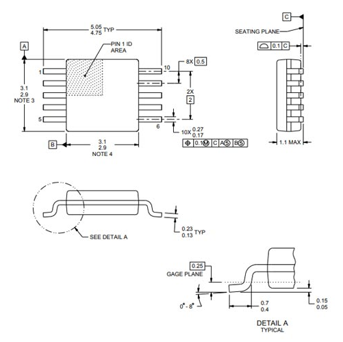
NOTES:
• All linear dimensions are in millimeters. Any dimensions in parentheses are for reference only. Dimensioning and tolerancing are per ASME Y14.5M.
• This drawing is subject to change without notice.
• This dimension does not include mold flash, protrusions, or gate burrs. Mold flash, protrusions, or gate burrs shall not exceed 0.15 mm per side.
• This dimension does not include interlead flash. Interlead flash shall not exceed 0.25 mm per side.
• Reference: JEDEC registration MO-187, variation BA.
About us
ALLELCO LIMITED
Read more
Quick inquiry
Please send an inquiry, we will respond immediately.
Comprehensive Guide to the AD736 True RMS-to-DC Converter IC
on December 26th
INA333 Instrumentation Amplifier: Alternatives, Pinout, and Applications
on December 26th
Popular Posts
-

Complex Instruction Set Computers: How They Changed Computing?
on April 18th 147749
-

USB-C Pinout and Features
on April 18th 111896
-

Using Xilinx Unified Simulation Primitives: A Comprehensive Guide to FPGA Design and Simulation
on April 18th 111349
-

Power Supply Voltages in Electronics: Meaning of VCC, VDD, VEE, VSS, and GND
on April 18th 83713
-

RJ45 Connector Guide: Pinout, Wiring, Cable Types, and Uses
on January 1th 79502
-

The Ultimate Guide to Wire Color Codes in Modern Electrical Systems
The way our electrical systems use colors isn’t just for looks. Each wire color now indicates a specific function, making it easier to identify and handle electrical components correctly during ins...on January 1th 66866
-

Quality (Q) Factor: Equations and Applications
The quality factor, or 'Q', is important when checking how well inductors and resonators work in electronic systems that use radio frequencies (RF). 'Q' measures how well a circuit minimizes energy...on January 1th 63003
-

Purge Valve Guide: Function, Symptoms, Testing, and Replacement for Optimal Engine Performance
The purge valve is a key part of a car’s system that helps keep the air clean by managing fuel vapors before they can escape into the atmosphere. This not only helps the environment by reducing pol...on January 1th 62934
-

Achieving Peak Performance with the Maximum Power Transfer Theorem
The Maximum Power Transfer Theorem explains how energy from a source, such as a battery or generator, flows to a connected load. It shows the exact condition where the load receives the most power....on January 1th 54073
-

A23 Battery Specifications and Compatibility
The A23 battery is a small, cylinder-shaped battery with high voltage. Also called 23A, 23AE, or MN21, it runs at 12 volts and much higher than AA or AAA batteries. Its special design make...on January 1th 52087
HOT Part Number
-
MAX208ECNG+
Analog Devices Inc./Maxim Integrated
IC TRANSCEIVER FULL 4/4 24DIP
ADP5022ACBZ-4-R7
Analog Devices Inc.
IC REG TRPL BCK/LNR SYNC 16WLCSP
DS1217A-64K-25
Analog Devices Inc./Maxim Integrated
MODULE NVRAM 8KB 250NS CARTRIDGE
AD5744RCSUZ
Analog Devices Inc.
IC DAC 14BIT V-OUT 32TQFP
TLC7528CNS
Texas Instruments
IC DAC 8BIT A-OUT 20SO
06035A910JAT2A
KYOCERA AVX
CAP CER 91PF 50V NP0 0603
FAN4800AUN
onsemi
IC PFC CTR AV CURR 268KHZ 16DIP
RR264MM-400TR
Rohm Semiconductor
DIODE GEN PURP 400V 1A PMDU
TMP106YZCT
Texas Instruments
SENSOR DIGITAL -40C-125C 6DSBGA
MCT06030C1002FP500
Electro-Films (EFI) / Vishay
RES SMD 10K OHM 1% 1/8W 0603
DMN6068LK3Q-13
Diodes Incorporated
MOSFET BVDSS: 41V 60V TO252
ADS7845E/2K5G4
Texas Instruments
IC SCREEN CNTRL 12BIT 16SSOP
XC4005E-3PQ100I
AMD
IC FPGA 77 I/O 100QFP
1812HC821KAT3A\SB
KYOCERA AVX
CAP CER 820PF 3KV X7R 1812
NRVTS12100PFST3G
onsemi
DIODE SCHOTTKY 100V 12A TO277-3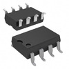
6N135-500E
Broadcom Limited
OPTOISO 3.75KV TRANS W/BASE 8SMD
MAX333AEUP+T
Analog Devices Inc./Maxim Integrated
IC SWITCH SPDT X 4 45OHM 20TSSOP
LFB212G45CG1C187
Murata Electronics
RF-D -

SC1565IST18TRT
Semtech Corporation
IC REG LINEAR 1.8V 1.5A SOT223-3
AD5220BN10
Analog Devices Inc.
IC POT DGTL 10K 128POS 8-DIP
LM2904AVQPWRG4
Texas Instruments
IC OPAMP GP 2 CIRCUIT 8TSSOP
BTF3125EJXUMA1
Infineon Technologies
IC PWR SWITCH N-CHAN 1:1 TDSO-8
744773115
Würth Elektronik
FIXED IND 15UH 1.2A 235 MOHM SMD
LP2981AIM5X-2.9
Texas Instruments
IC REG LINEAR FIXED LDO REG
1808SC102MAJ1A
KYOCERA AVX
CAP CER 1000PF 1.5KV X7R 1808
DS89C420-MNL
Analog Devices Inc./Maxim Integrated
IC MCU 8BIT 16KB FLASH 40DIP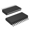
STP16DPS05MTR
STMicroelectronics
IC LED DRIVER LINEAR 100MA 24SO
VC060305A150DP
KYOCERA AVX
VARISTOR 8.5V 30A 0603
CSD16410Q5A
Texas Instruments
MOSFET N-CH 25V 16A/59A 8VSON
HAL1000UT-K
TDK-Micronas GmbH
MAGNETIC SWITCH PROG TO92UT
SI1403BDL-T1-GE3
Vishay Siliconix
MOSFET P-CH 20V 1.5A SC70-6
AD7999YRJZ-1500RL7
Analog Devices Inc.
IC ADC 8BIT SAR SOT23-8
EP2A15B724C7
Intel
IC FPGA 492 I/O 724BGA
SN74AHC138RGYR
Texas Instruments
IC DECODER/DEMUX 1X3:8 16VQFN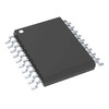
PIC16F627A-I/SS
Microchip Technology
IC MCU 8BIT 1.75KB FLASH 20SSOP
MAX98307ETE+T
Analog Devices Inc./Maxim Integrated
IC AMP CLASS DG MONO 3.3W 16TQFN -

AOB290L
Alpha & Omega Semiconductor Inc.
MOSFET N-CH 100V 18A/140A TO263
MAX13433EETD+T
Analog Devices Inc./Maxim Integrated
IC TRANSCEIVER FULL 1/1 14TDFN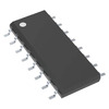
SN74LVC112ADR
Texas Instruments
IC FF JK TYPE DUAL 1BIT 16SOIC
ATSAM4SD32BA-MU
Microchip Technology
IC MCU 32BIT 2MB FLASH 64QFN
CL31A106KPHNNNF
Samsung Electro-Mechanics
CAP CER 10UF 10V X5R 1206
SOLC-120-02-F-Q-A
Samtec Inc.
CONN RCPT 80POS 0.05 GOLD SMD
UPW1J101MPD
Nichicon
CAP ALUM 100UF 20% 63V RADIAL
CS5532-BSZR
Cirrus Logic Inc.
IC ADC 24BIT SIGMA-DELTA 20SSOP
CC0603GRNPO9BN120
YAGEO
CAP CER 12PF 50V C0G/NPO 0603
S-812C50AMC-C3ET2G
ABLIC Inc.
IC REG LINEAR 5V 75MA SOT23-5
C3216X8R1H684M160AE
TDK Corporation
CAP CER 0.68UF 50V X8R 1206
CY2309NZSC-1HT
Cypress Semiconductor Corp
IC CLK BUF 1:9 133.3MHZ 16SOIC
FDD6632
Fairchild Semiconductor
MOSFET N-CH 30V 9A DPAK
GCM155R71E473KA55D
Murata Electronics
CAP CER 0.047UF 25V X7R 0402
LM2743MTCX
Texas Instruments
IC REG CTRLR BUCK 14TSSOP
7440650047
Würth Elektronik
FIXED IND 4.7UH 4.6A 23 MOHM SMD
SS2P4HM3/84A
Vishay General Semiconductor - Diodes Division
DIODE SCHOTTKY 40V 2A DO220AA
V24C12H100BS
Vicor Corporation
DC DC CONVERTER 12V 100W