A Practical Guide to the EPF10K30AFC484-1 FPGA Chip
Working with digital systems becomes easier when you understand how a programmable logic device fits into the design. The EPF10K30AFC484-1 belongs to the FLEX 10KA FPGA family and offers configurable logic, internal memory, and flexible signal routing inside a single chip. You can use it to manage control logic, coordinate signals, or build custom digital functions without changing the physical hardware. Its structure supports complex system layouts while maintaining reliable data flow. By exploring its architecture, features, and applications, you gain a clearer picture of how this FPGA supports many types of electronic systems.Catalog

EPF10K30AFC484-1 Overview
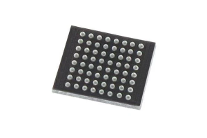
EPF10K30AFC484-1 is a field programmable gate array used to implement configurable digital logic in embedded electronic systems. The device contains programmable logic elements, internal memory blocks, and routing resources that allow custom digital functions to be created within a single component. Its internal structure supports control logic, data handling, and interface management across a wide range of electronic equipment. The device operates from a 4.75 V to 5.25 V supply range and provides up to 246 programmable input and output connections. The package uses a 484 ball fine pitch BGA format suitable for surface mounted circuit boards in compact system designs.
Looking for EPF10K30AFC484-1? Contact us to check current stock, lead time, and pricing.
SameFrame Pin-Out Example of EPF10K30AFC484-1
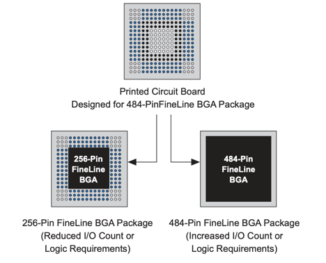
Package layout demonstrates how devices in the FLEX 10K family share a consistent ball grid structure across different package sizes. A printed circuit board footprint designed for a 484 pin FineLine BGA package supports devices with different I/O counts by maintaining the same outer ball positions. The diagram compares a 256 pin FineLine BGA device and a 484 pin FineLine BGA device, where the smaller package uses a reduced number of active connections while keeping alignment with the same board layout. This arrangement allows circuit boards designed for the larger package to accommodate smaller versions of the device when fewer input or output signals or logic resources are required.
Features of EPF10K30AFC484-1
Programmable Logic Architecture
The device integrates a programmable logic structure that allows digital circuits to be configured after installation. Designers can implement control logic, signal routing, and processing functions inside the chip by defining connections between internal logic elements.
Logic Element Organization
A total of 1728 logic elements are arranged into multiple logic array blocks that form the internal processing structure. Each logic element can perform arithmetic, combinational logic, or storage operations, allowing the device to support a wide range of digital circuit designs.
Embedded Memory Blocks
The device includes 12288 bits of internal memory organized in dedicated array blocks. These blocks provide on chip data storage that can be configured for temporary buffering, lookup tables, or small memory functions used by digital systems.
Flexible Input and Output Interface
Up to 246 programmable input and output connections allow the device to communicate with external components. These connections support bidirectional signal paths and can be configured for different digital interface requirements.
Structured Routing Network
Signals move through the device using a routing structure formed by row and column interconnect paths. This internal network distributes data between logic blocks, memory areas, and input output pins across the programmable array.
Stable Operating Voltage Range
The device operates from a 4.75 V to 5.25 V supply range that aligns with many digital electronic systems. This voltage range supports reliable signal behavior during continuous system operation.
Standard Commercial Temperature Operation
Designed for commercial temperature environments, the device functions across a temperature range of 0°C to 70°C. This operating window supports indoor electronic equipment and controlled system environments.
Surface Mount FBGA Package
The component is housed in a 484 ball fine pitch BGA package measuring approximately 23 by 23 millimeters. This format supports dense circuit layouts while maintaining stable electrical connections on multilayer printed circuit boards.
| Product Attribute | Attribute Value |
| Manufacturer | Altera (Intel) |
| Voltage - Supply | 4.75V ~ 5.25V |
| Total RAM Bits | 12288 |
| Supplier Device Package | 484-FBGA (23x23) |
| Series | FLEX-10KA® |
| Package / Case | 484-BBGA |
| Package | Bulk |
| Operating Temperature | 0°C ~ 70°C (TA) |
| Number of Logic Elements/Cells | 1728 |
| Number of LABs/CLBs | 216 |
| Number of I/O | 246 |
| Number of Gates | 69000 |
| Mounting Type | Surface Mount |
| RoHS Status | RoHS non-compliant |
| Moisture Sensitivity Level (MSL) | 3 (168 Hours) |
| REACH Status | REACH Unaffected |
| ECCN | 3A991D |
| HTSUS | 8542.39.0001 |
Device Block Diagram of EPF10K30AFC484-1
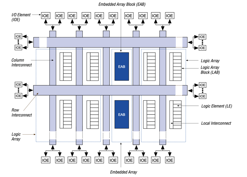
Internal layout arranges programmable logic across a grid of Logic Array Blocks that contain multiple logic elements used to build digital circuits. Embedded Array Blocks appear within the array and provide dedicated memory resources that store data during device operation. Horizontal and vertical routing channels labeled as row and column interconnects form the internal signal network that links the logic blocks and memory regions. Input and output elements are positioned around the outer edges of the device, creating the electrical interface between internal logic and external pins. Local interconnect paths inside each logic array block allow nearby logic elements to exchange signals quickly, while the larger routing structure distributes signals across the entire programmable array.
Embedded Array Block of EPF10K30AFC484-1
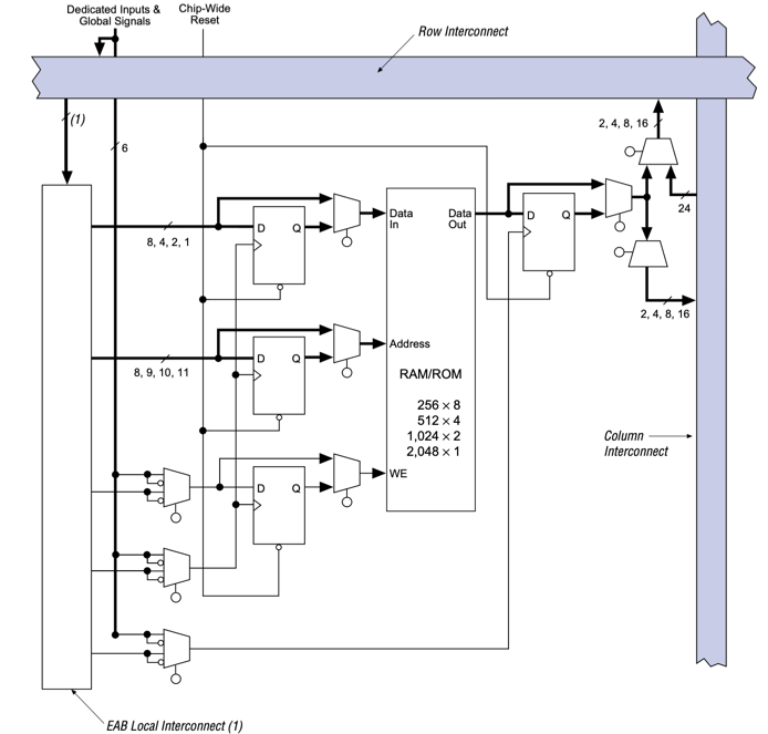
Memory structure inside the programmable array contains an Embedded Array Block that provides dedicated storage within the FPGA fabric. The block supports configurable memory sizes including 256 × 8, 512 × 4, 1,024 × 2, and 2,048 × 1, allowing flexible data width and depth arrangements depending on the design. Data input, data output, address selection, and write enable paths connect the memory cell to surrounding logic through internal registers and control multiplexers. Local interconnect lines route signals from nearby logic array blocks directly into the memory interface, while row and column interconnect channels link the block to the wider routing network across the device. Dedicated input paths and global control signals manage timing and synchronization so stored data can be accessed by programmable logic elements within the FPGA.
Applications of EPF10K30AFC484-1
Industrial Control Systems
The device can manage digital control tasks within automated equipment. Programmable logic allows system designers to implement timing control, sensor processing, and actuator coordination within industrial machines and production systems.
Digital Signal Processing Platforms
Embedded logic resources and internal memory allow the device to support signal manipulation and filtering tasks. It can be used in systems that process sampled data streams, where digital operations must occur in predictable time intervals.
Telecommunications Interface Control
Communication equipment often requires configurable logic to manage protocol handling and signal routing. The device can coordinate data paths between communication channels and digital processing units within networking equipment.
Data Acquisition Equipment
Electronic measurement systems collect signals from multiple sensors and convert them into digital data streams. The device can manage signal timing, buffering, and interface control in systems used for monitoring and measurement.
Network Communication Hardware
Network interface equipment uses programmable logic to manage packet handling and internal signal coordination. The device can organize data paths between processing units and external communication interfaces.
Digital System Prototyping Platforms
Development systems often use programmable logic devices to test and evaluate digital circuit designs. The device allows engineers and developers to verify system behavior before committing designs to fixed hardware implementations.
Advantages and Disadvantages of EPF10K30AFC484-1
Advantages
• High I/O pin count enables connection with many external components in complex systems
• Large number of logic elements allows implementation of sophisticated digital logic circuits
• Embedded RAM supports internal data buffering and memory operations
• Programmable architecture allows design changes without modifying hardware layout
• Surface mount FBGA package supports compact circuit board integration
• Suitable for custom hardware acceleration and parallel logic processing
Disadvantages
• Requires specialized FPGA development tools and hardware design knowledge
• Higher power consumption compared with smaller programmable logic devices
• Older FPGA family with lower efficiency compared with modern FPGA architectures
• Development and debugging process can be complex for beginners
EPF10K30AFC484-1 Alternatives
| Part Number | Manufacturer | Key Features | Use Case/Notes |
| EPF10K30AFC484-2 | Intel | Member of the FLEX-10KA FPGA family with about 1,728 logic elements and 12,288 bits of embedded RAM. Provides up to 246 I/O pins and supports a 5 V supply range. The device allows designers to implement programmable digital logic functions inside a single integrated circuit. | Commonly used in industrial control systems, telecommunications hardware, and embedded computing platforms where configurable logic is needed for custom digital processing. |
| EPF10K30AFC484-3 | Intel | FPGA device based on the FLEX-10KA architecture with programmable logic blocks, internal RAM resources, and a high pin-count interface. It enables designers to configure digital circuits without producing a custom ASIC. | Often applied in communication equipment, signal processing boards, and prototype digital systems where hardware flexibility is required during development. |
| EPF10K30AFC484-3 | Altera | High density programmable logic device from the FLEX-10KA series combining configurable logic cells, embedded memory blocks, and flexible routing resources. The architecture supports complex digital designs with large gate capacity. | Suitable for telecommunications systems, embedded processing hardware, and custom digital control boards where programmable logic replaces fixed hardware circuits. |
About Altera (Intel)
Altera was a semiconductor company known for designing programmable logic devices used in digital electronic systems. The company developed a wide range of field programmable gate arrays and programmable logic components used in communications, computing, industrial equipment, and embedded platforms. Its products allowed designers to create custom digital circuits that could be reconfigured after manufacturing. Altera introduced several programmable logic families including MAX, FLEX, and Stratix devices that became widely used in electronic design. The company later became part of Intel, where its programmable logic technology continues to be developed for data processing, networking systems, and embedded digital platforms.
Conclusion
Understanding the EPF10K30AFC484-1 helps you see how programmable logic can simplify complex digital systems. This device combines configurable logic elements, internal memory, and flexible routing so you can build custom logic functions inside a single component. You also saw how its package structure, device architecture, and embedded memory blocks support reliable data movement across a circuit. Its applications span industrial control, signal processing, communication equipment, and system prototyping. By reviewing its features and design structure, you gain a clearer idea of how this FPGA can support adaptable and efficient electronic system development.
About us
ALLELCO LIMITED
Read more
Quick inquiry
Please send an inquiry, we will respond immediately.
Frequently Asked Questions [FAQ]
1. What type of device is the EPF10K30AFC484-1?
The EPF10K30AFC484-1 is a field programmable gate array that allows digital logic circuits to be configured after the device is installed in a system.
2. How many input and output connections does the EPF10K30AFC484-1 support?
The device supports up to 246 programmable input and output connections that allow communication with external components in a circuit.
3. What is the operating voltage range of the EPF10K30AFC484-1?
The device operates within a supply voltage range of 4.75 V to 5.25 V, which aligns with many digital electronic systems.
4. What internal memory does the EPF10K30AFC484-1 contain?
The device includes embedded memory blocks that provide 12,288 bits of storage for buffering data and supporting internal logic operations.
5. Where is the EPF10K30AFC484-1 commonly used?
It is often used in industrial control systems, communication equipment, data acquisition hardware, and digital system prototyping platforms.
XCV200E-6FG256C Device Overview and Functional Structure
on March 13th
Inside the S29GL256N11FFI020 NOR Flash Storage Device
on March 13th
Popular Posts
-

Complex Instruction Set Computers: How They Changed Computing?
on April 17th 147713
-

USB-C Pinout and Features
on April 17th 111731
-

Using Xilinx Unified Simulation Primitives: A Comprehensive Guide to FPGA Design and Simulation
on April 17th 111322
-

Power Supply Voltages in Electronics: Meaning of VCC, VDD, VEE, VSS, and GND
on April 17th 83611
-

RJ45 Connector Guide: Pinout, Wiring, Cable Types, and Uses
on January 1th 79265
-

The Ultimate Guide to Wire Color Codes in Modern Electrical Systems
The way our electrical systems use colors isn’t just for looks. Each wire color now indicates a specific function, making it easier to identify and handle electrical components correctly during ins...on January 1th 66780
-

Quality (Q) Factor: Equations and Applications
The quality factor, or 'Q', is important when checking how well inductors and resonators work in electronic systems that use radio frequencies (RF). 'Q' measures how well a circuit minimizes energy...on January 1th 62947
-

Purge Valve Guide: Function, Symptoms, Testing, and Replacement for Optimal Engine Performance
The purge valve is a key part of a car’s system that helps keep the air clean by managing fuel vapors before they can escape into the atmosphere. This not only helps the environment by reducing pol...on January 1th 62829
-

Achieving Peak Performance with the Maximum Power Transfer Theorem
The Maximum Power Transfer Theorem explains how energy from a source, such as a battery or generator, flows to a connected load. It shows the exact condition where the load receives the most power....on January 1th 54028
-

A23 Battery Specifications and Compatibility
The A23 battery is a small, cylinder-shaped battery with high voltage. Also called 23A, 23AE, or MN21, it runs at 12 volts and much higher than AA or AAA batteries. Its special design make...on January 1th 51992
HOT Part Number
-

RT9742BGJ5F
Richtek USA Inc.
IC PWR SWITCH N-CH 1:1 TSOT23-5
MC9S08JM60CLD
NXP USA Inc.
IC MCU 8BIT 60KB FLASH 44LQFP
AP7344-3318RH4-7
Diodes Incorporated
IC REG LIN 1.8V/3.3V X2DFN1612-8
1808AC103MAT2A
KYOCERA AVX
CAP CER 10000PF 1KV X7R 1808
TSV324IYPT
STMicroelectronics
IC OPAMP GP 4 CIRCUIT 14TSSOP
MT46H64M16LFBF-6 IT:B
Micron Technology Inc.
IC DRAM 1GBIT PARALLEL 60VFBGA
MM3Z47VC
onsemi
DIODE ZENER 47V 200MW SOD323F
MC74HC27DR2
onsemi
NOR GATE, HC/UH SERIES, 3-FUNC,
1812CC472KAT9A
KYOCERA AVX
CAP CER 4700PF 630V X7R 1812
TPS72018DRVR
Texas Instruments
IC REG LINEAR 1.8V 350MA 6WSON
EV2400
Texas Instruments
EVAL MODULE INTERFACE BOARD
R46KI310050M1K
KEMET
CAP FILM 0.1UF 10% 560VDC RADIAL
P3104UCMCRP
Littelfuse Inc.
THYRISTOR 275V/550V 400A 6SMD GW
UMK105CG150JW-F
Taiyo Yuden
CAP CER 15PF 50V C0G/NP0 0402
SP8M24FU7TB1
Rohm Semiconductor
MOSFET N/P-CH 8SOP
AH3764Q-W-7
Diodes Incorporated
MAGNETIC SWITCH LATCH SC59
HIP6012CB-T
Renesas Electronics America Inc
IC REG CTL INTEL PWM 1OUT 14SOIC
GRM0335C2A2R6CA01D
Murata Electronics
CAP CER 2.6PF 100V C0G/NP0 0201 -

DB2J31600L
Panasonic Electronic Components
DIODE SCHOT 30V 100MA SMINI2
PIC16C73B-20I/SS
Microchip Technology
IC MCU 8BIT 7KB OTP 28SSOP
AD8390ACP-REEL7
Analog Devices Inc.
IC AMP DIFF LP LDIST 16LFCSP
MC9S08AC96CFUE
NXP USA Inc.
IC MCU 8BIT 96KB FLASH 64QFP
MMSZ4692T1
onsemi
DIODE ZENER 6.8V 500MW SOD123
MAX509BCAP+
Analog Devices Inc./Maxim Integrated
IC DAC 8BIT QUAD R-R 20-SSOP
IXFA180N10T2
IXYS
MOSFET N-CH 100V 180A TO263
LE33ABZ
STMicroelectronics
IC REG LINEAR 3.3V 100MA TO92-3
CL31C470JIFNNNF
Samsung Electro-Mechanics
CAP CER 47PF 1KV NP0 1206
MC74ACT377N
onsemi
IC FF D-TYPE SNGL 8BIT 20DIP
AD694ARZ-REEL
Analog Devices Inc.
IC TRANSMITTER 4-20MA 16-SOIC
EK508V-03P
Dinkle Corporation, USA
TERM BLK 3POS 5.00MM SCRW PLG
AWK105C6105MP-F
Taiyo Yuden
CAP CER 1UF 4V X6S 0204
SS5P9HM3_A/H
Vishay General Semiconductor - Diodes Division
DIODE SCHOTTKY 90V 5A TO277A
LTC1772CS6#TRPBF
Analog Devices Inc.
IC REG CTRLR MULT TOP SOT23-6
178.6165.0002
Littelfuse Inc.
FUSE HOLDER BLADE 80V PCB
TL431BIDR2
onsemi
IC VREF SHUNT ADJ 0.4% 8SOIC
ISL6613ECB
Renesas Electronics America Inc
IC GATE DRVR HALF-BRIDGE 8SOIC -

C1608JB1E475M080AC
TDK Corporation
CAP CER 4.7UF 25V JB 0603
CHB50W-24S05
Cincon Electronics Co. LTD
DC DC CONVERTER 5V 50W
TDA7479ADTR
STMicroelectronics
RF DEMODULATOR IC 16TSSOP
LQH2HPN100MG0L
Murata Electronics
FIXED IND 10UH 490MA 876MOHM SMD
AD6654CBC
Analog Devices Inc.
IC ADC 14BIT W/4CH RSP 256CSPBGA
BD3520FVM-TR
Rohm Semiconductor
IC LNR REG CTRLR 1OUT 8MSOP
CL21B471KBANNNC
Samsung Electro-Mechanics
CAP CER 470PF 50V X7R 0805
CL10A106MR8NNNC
Samsung Electro-Mechanics
CAP CER 10UF 4V X5R 0603
SFS4-DC24V
Panasonic Electric Works
RELAY SAFETY 6PST 6A 24V
TPS53631RSBR
Texas Instruments
IC REG CTRLR VR12 1OUT 40WQFN
GRM0225C1E8R9DDAEL
Murata Electronics
CAP CER 8.9PF 25V C0G/NP0 01005
ISO7240MDWR
Texas Instruments
DGTL ISO 2500VRMS 4CH GP 16SOIC
MC74ACT14DR2
onsemi
IC SCHMITT TRIG HEX INV 14-SOIC
TPSMB200CA
Littelfuse Inc.
TVS DIODE 171VWM 274VC DO214AA
TLP754(F)
Toshiba Semiconductor and Storage
OPTOISO 5KV OPEN COLLECTOR 8DIP
AD7545AUE
Analog Devices Inc.
IC DAC 12BIT A-OUT 20LCCC
170M5408
Eaton - Bussmann Electrical Division
FUSE SQUARE 400A 700VAC RECT
ISL8105BCRZ-T
Renesas Electronics America Inc
IC REG CTRLR BUCK 10DFN