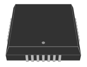
ADM5170AP Line Driver Guide: Features, Pinout, Applications and RS-232/RS-423 Signal Conversion
This guide is all about the ADM5170AP, a special chip that helps send signals in digital communication systems. It focuses on how this chip takes basic logic signals (like TTL or CMOS) and converts them into stronger RS-232 or RS-423 signals for better transmission. It also explains how the ADM5170AP allows you to select the output mode, adjust the signal speed, and use it efficiently. It highlights how this chip makes it easier to connect and send data clearly and reliably over longer distances.Catalog
ADM5170AP Overview
The ADM5170AP is a versatile octal line driver tailored for digital communication systems, handling data rates up to 116 kB/s. It is uniquely engineered to accept TTL or CMOS inputs, which are then inverted and translated into RS-232E or RS-423A signal levels. This flexibility is governed by the Mode Select inputs MS+ and MS–; setting both to GND initiates RS-423 operation, whereas connecting MS+ to VDD and MS– to VSS enables RS-232 operation. The output slew rate can be finely adjusted from 10 V/µs to 2.2 V/µs by connecting an external resistor between the Slew Rate Adjust (SRA) pin and GND, accommodating various cable lengths and types. The device also features outputs that can be disabled using the EN (Enable Input) pin, allowing the sharing of a common output line which enhances system design flexibility and efficiency. The ADM5170AP integrates low power CMOS technology, output short circuit protection, and TTL/CMOS compatible inputs, making it an ideal choice for high-speed modems, computer I/O ports, and logic level translation applications.
If you're thinking about upgrading your systems or expanding your product line, the ADM5170AP is a smart choice. Contact us today to place your bulk order and ensure your inventory meets demand with this high-performance component.
ADM5170AP Pin Configuration
|
Mnemonic |
Function |
|
VDD |
Power Supply Input, +10 V ± 10%. |
|
VSS |
Power Supply Input, –10 V ± 10%. |
|
GND |
Ground Pin. Must be connected to 0 V. |
|
AI . . . HI |
Digital Input to Drivers A to H. |
|
AO . . . HO |
RS-232/RS-423 Output from Drivers A to H. |
|
EN |
Enable Pin. When high, all outputs are 3-stated. |
|
MS+, MS– |
Mode Select Inputs. Used to control the output level
swing. With MS+ & MS- connected to GND, RS-423A output levels are selected. With
MS+ connected to VDD and
MS– connected to VSS, RS-232
output levels are developed. |
|
SRA |
Slew Rate Adjust Input. An external resistor (2 kΩ to 10
kΩ) connected between this pin and GND is used to control the Output Slew
Rate (10 V/µs to 2.2 V/µs). |
ADM5170AP CAD Models
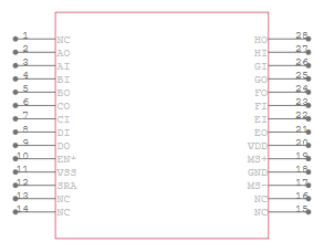
ADM5170AP Symbol
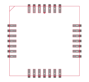
ADM5170AP Footprint
ADM5170AP 3D Model
ADM5170AP Features
• Eight Single-Ended Line Drivers: The ADM5170AP includes eight independent line drivers in one package, allowing for multiple channels of data transmission simultaneously. This feature is useful for complex digital communication systems that require multiple signal outputs
• Standards Compliance: This device is compliant with EIA RS-232E, RS-423A, and CCITT V.10/X.26 standards, ensuring it can operate smoothly within a range of digital communication frameworks and is compatible with international communication protocols.
• Programmable Slew Rate: You can adjust the output slew rate from 10 V/µs to 2.2 V/µs by connecting an external resistor between the Slew Rate Adjust (SRA) pin and ground. This adjustability allows for fine-tuning of signal integrity according to the characteristics of the connecting cable, reducing signal reflections and transmission errors.
• Wide Supply Voltage Range: The ADM5170AP operates with a supply voltage range from 9 V to 15 V for VDD and from –9 V to –15 V for VSS. This broad range accommodates various power supplies, enhancing the device's flexibility in different system configurations.
• Low Power CMOS Technology: Built with low power CMOS technology, the ADM5170AP reduces power consumption down to 40 mW when disabled. This feature is important for energy-saving in systems that require long operational hours and sustainability.
• 3-State Outputs: The output pins of the ADM5170AP can be disabled using the EN (Enable Input) pin. This functionality allows for the sharing of common communication lines and prevents signal interference, making it ideal for systems where multiple drivers share output pathways.
• TTL/CMOS Compatible Inputs: The line driver accepts both TTL and CMOS input levels, offering versatility in interfacing with various logic families. This feature simplifies the design process by eliminating the need for additional level shifting hardware.
• Output Short Circuit Protection: It includes built-in protection against output shorts, which enhances the reliability and durability of the device by preventing damage due to accidental short circuits during operation.
ADM5170AP Block Diagram
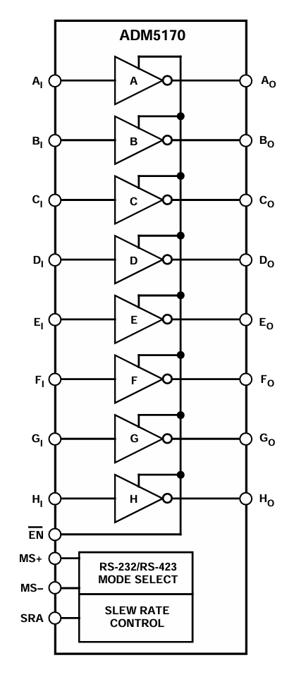
The block diagram of the ADM5170AP illustrates its function as an octal line driver, handling eight input-output signal channels labeled A through H. Each signal input (AI to HI) passes through a dedicated inverting line driver, which converts TTL/CMOS input signals into appropriate line driver output levels (AO to HO). These outputs can operate under either RS-232 or RS-423 standards, depending on the mode selected via the MS+ and MS– pins. The Mode Select block at the bottom of the diagram switches between RS-232 and RS-423 signaling levels.
Additionally, the diagram shows a Slew Rate Control pin (SRA), which allows the to adjust the transition rate of the output signals. This helps manage signal integrity and electromagnetic interference (EMI), particularly over longer transmission lines. The EN pin is an enable control that activates or disables all drivers simultaneously. Overall, the ADM5170AP is a versatile line driver IC used in digital communication systems, designed to support multiple standards and ensure reliable signal transmission over serial data links.
ADM5170AP Specifications
|
Type |
Parameter |
|
Manufacturer |
Analog Devices Inc. |
|
Packaging |
Tube |
|
Part Status |
Obsolete |
|
Type |
Driver |
|
Protocol |
RS232, RS423 |
|
Number of Drivers/Receivers |
8/0 |
|
Data Rate |
116Kbps |
|
Voltage - Supply |
9V ~ 15V |
|
Operating Temperature |
-40°C ~ 85°C |
|
Mounting Type |
Surface Mount |
|
Package / Case |
28-LCC (J-Lead) |
|
Supplier Device Package |
28-PLCC (11.51x11.51) |
|
Base Product Number |
ADM5170 |
ADM5170AP Output Mode Programming
The ADM5170AP chip has two output modes that let it work with different voltage standards for sending signals. These modes are:
1. Low Output Mode: This mode follows the RS-423A standard, which is used for straightforward, point-to-point communications. To use this mode, connect the mode select pins, labeled MS+ and MS–, directly to the ground (GND). This setup keeps the voltage levels lower and more controlled, which is good for avoiding interference when lines are close together.
2. High Output Mode: This mode matches the RS-232 standard and is suitable for scenarios where cables are long or the signal has to travel far, as it allows for stronger and higher voltage signals. To activate this mode, connect MS+ to the positive power supply (VDD) and MS– to the negative power supply (VSS). This makes the output stronger, ensuring the signal stays clear over longer distances.
|
Inputs |
Outputs |
|||
|
MS+ |
MS– |
EN |
Data |
|
|
GND |
GND |
0 |
0 |
5 V to 6 V (RS-423) |
|
GND |
GND |
0 |
1 |
–5 V to –6 V (RS-423) |
|
VDD |
VSS |
0 |
0 |
(VDD – 3 V) (RS-232)¹ |
|
VDD |
VSS |
0 |
1 |
(VSS + 3 V) (RS-232)¹ |
|
X |
X |
1 |
X |
High Z |
ADM5170AP Applications
High-Speed Communication Systems
The ADM5170AP is ideally suited for high-speed communication systems due to its capacity to handle data rates up to 116 kB/s. This makes it perfect for applications requiring rapid and reliable data transmission over networks.
Computer I/O Ports and Peripherals
This line driver is used extensively in interfacing computer input/output ports and peripherals. Its compatibility with TTL/CMOS levels and RS-232E/RS-423A standards ensures it can seamlessly integrate with a wide range of computer hardware, enhancing connectivity and data flow between devices.
High-Speed Modems
Given its high data rate handling and adjustable slew rate, the ADM5170AP is an excellent choice for high-speed modem applications. It helps modulate and demodulate data signals effectively, ensuring clear and consistent internet connectivity.
Printers
In printers, the ADM5170AP helps in the reliable transmission of data between the computer and the printer. Its ability to transmit data effectively over longer distances without loss ensures high-quality, fast printing operations.
Logic Level Translation
The device also plays a role in logic level translation, converting TTL or CMOS input levels into RS-232E or RS-423A output levels. This function is good in systems where devices operate at different logic levels, ensuring compatibility and effective communication across diverse electronic components.
ADM5170AP Similar Parts
ADM5170AP Advantages
Dual Protocol Support with Mode Select
The ADM5170AP allows to select between RS-232E and RS-423A output standards using Mode Select inputs (MS+ and MS–). This dual compatibility offers flexibility in application design, accommodating various communication requirements without the need for additional components.
Eight Independent Drivers
Integrating eight single-ended line drivers into one package, the ADM5170AP minimizes the need for multiple chips, saving space and reducing complexity in system design. This integration is beneficial in environments with limited PCB real estate.
Wide Supply Voltage Range
The device's ability to operate across a wide supply voltage range (9 V to 15 V for VDD, and –9 V to –15 V for VSS) makes it adaptable to various power environments, enhancing its utility in diverse operational settings.
Low Power Consumption
Featuring low power CMOS technology, the ADM5170AP consumes less power, especially when disabled (only 40 mW). This energy efficiency makes it suitable for applications where power conservation is needed, such as battery-operated devices.
TTL/CMOS Compatible Inputs
Its compatibility with standard TTL and CMOS logic levels ensures the ADM5170AP can seamlessly interface with a broad range of digital systems, eliminating the need for level-shifting hardware and simplifying system design.
Output Short Circuit Protection
With built-in protection against output shorts, the ADM5170AP provides enhanced durability and reliability, protecting the device and the system from damage caused by accidental short circuits during operation.
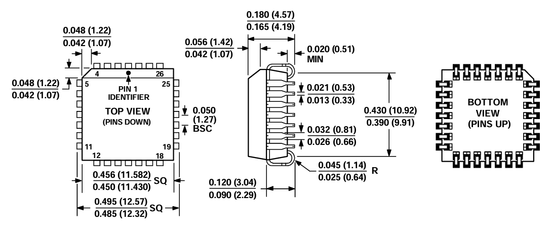
ADM5170AP Packaging Dimensions
Package Dimensions
|
Parameter |
Dimension (mm) |
|
Body Width (Min – Max) |
12.32 – 12.57 |
|
Body Length (Min – Max) |
11.43 – 11.58 |
|
Body Height (Min – Max) |
9.91 – 10.92 |
|
Lead Span (Min – Max) |
4.19 – 4.57 |
|
Lead Pitch (Typical) |
1.27 |
|
Lead Thickness (Min – Max) |
0.33 – 0.53 |
|
Lead Width (Min – Max) |
0.64 – 1.14 |
|
Standoff Height (Min) |
0.51 |
|
Lead Shoulder Width (Min – Max) |
1.07 – 1.42 |
|
Corner Radius (R) (Min – Max) |
0.64 – 1.14 |
Package Outline
ADM5170AP Manufacturer
The ADM5170AP is manufactured by Analog Devices Inc. (ADI), a globally recognized leader in the design and production of high-performance analog, mixed-signal, and digital signal processing (DSP) integrated circuits. Founded in 1965 and headquartered in Wilmington, Massachusetts, ADI is known for delivering cutting-edge semiconductor solutions that serve applications across industries such as communications, industrial automation, automotive systems, and consumer electronics. ADI’s reputation for reliability and innovation is reflected in components like the ADM5170AP, which showcases the company’s focus on signal integrity, low power consumption, and system flexibility. Analog Devices ensures that every product, including the ADM5170AP, meets stringent quality and performance standards for modern electronic systems.
Conclusion
The ADM5170AP offers a well-rounded solution for digital communication applications demanding robust signal conversion and protocol flexibility. With support for RS-232E and RS-423A standards, eight independent driver channels, and features like programmable slew rate and output enable control, it simplifies design integration across a wide range of systems. Its compatibility with TTL/CMOS inputs, low power operation, and built-in short-circuit protection further enhance its utility in power-sensitive and space-constrained environments. Backed by Analog Devices' reputation for quality and innovation, the ADM5170AP is a solid choice for those seeking dependable performance in serial communication applications.
Datasheet PDF
ADM5170AP Datasheets:
About us
ALLELCO LIMITED
Read more
Quick inquiry
Please send an inquiry, we will respond immediately.
Frequently Asked Questions [FAQ]
1. Can the ADM5170AP operate in noisy industrial environments?
Yes, the ADM5170AP is built with robust RS-232 and RS-423 signal standards that can handle longer cable runs and resist noise. The adjustable slew rate feature helps reduce EMI, which is great in industrial settings.
2. Is the ADM5170AP compatible with microcontrollers or logic ICs operating at 5V?
Yes. The chip accepts TTL and CMOS logic levels, making it fully compatible with 5V microcontrollers and other digital logic devices without needing level shifters.
3. Does the ADM5170AP need any external components to work properly?
At minimum, it requires external power supply connections and a resistor on the SRA pin if you want to control the slew rate. Otherwise, most functionality is integrated, simplifying setup.
4. What happens to the outputs when the EN pin is high?
When the EN (Enable) pin is driven high, all outputs are put into a high-impedance state. This feature is helpful when sharing output lines between multiple drivers to prevent conflicts.
5. How do I choose the right value for the slew rate adjustment resistor?
Use a resistor between 2 kΩ and 10 kΩ between the SRA pin and GND. A higher resistance slows the output transition speed, which is ideal for reducing EMI in longer cables.
What Capacitors Do in Electronic Circuits
on April 17th
GC5325IZND Chip Full Guide: Pinout, Features, Alternatives and Specifications
on April 17th
Popular Posts
-

Complex Instruction Set Computers: How They Changed Computing?
on April 18th 147778
-

USB-C Pinout and Features
on April 18th 112033
-

Using Xilinx Unified Simulation Primitives: A Comprehensive Guide to FPGA Design and Simulation
on April 18th 111352
-

Power Supply Voltages in Electronics: Meaning of VCC, VDD, VEE, VSS, and GND
on April 18th 83792
-

RJ45 Connector Guide: Pinout, Wiring, Cable Types, and Uses
on January 1th 79596
-

The Ultimate Guide to Wire Color Codes in Modern Electrical Systems
The way our electrical systems use colors isn’t just for looks. Each wire color now indicates a specific function, making it easier to identify and handle electrical components correctly during ins...on January 1th 66976
-

Purge Valve Guide: Function, Symptoms, Testing, and Replacement for Optimal Engine Performance
The purge valve is a key part of a car’s system that helps keep the air clean by managing fuel vapors before they can escape into the atmosphere. This not only helps the environment by reducing pol...on January 1th 63110
-

Quality (Q) Factor: Equations and Applications
The quality factor, or 'Q', is important when checking how well inductors and resonators work in electronic systems that use radio frequencies (RF). 'Q' measures how well a circuit minimizes energy...on January 1th 63043
-

Achieving Peak Performance with the Maximum Power Transfer Theorem
The Maximum Power Transfer Theorem explains how energy from a source, such as a battery or generator, flows to a connected load. It shows the exact condition where the load receives the most power....on January 1th 54097
-

A23 Battery Specifications and Compatibility
The A23 battery is a small, cylinder-shaped battery with high voltage. Also called 23A, 23AE, or MN21, it runs at 12 volts and much higher than AA or AAA batteries. Its special design make...on January 1th 52197
HOT Part Number
-
FMX-4202S
Sanken Electric USA Inc.
DIODE ARRAY GP 200V 20A TO3PF
LDS8620-002-T2
IXYS Integrated Circuits Division
IC LED DRV RGLTR PWM 96MA 16TQFN
MMSZ5230BS-7-F
Diodes Incorporated
DIODE ZENER 4.7V 200MW SOD323
LFXP2-8E-5FTN256I
Lattice Semiconductor Corporation
IC FPGA 201 I/O 256FTBGA
1SC0450E2A0-45
Power Integrations
IC GATE DRVR HI/LOW SIDE MODULE
SI3493DDV-T1-GE3
Vishay Siliconix
MOSFET P-CHANNEL 20V 8A 6TSOP
R3111Q341A-TR-FE
Nisshinbo Micro Devices Inc.
IC SUPERVISOR 1 CHANNEL SC82AB
DG409DVZ-T
Renesas Electronics America Inc
IC SWITCH SP4TX2 100OHM 16TSSOP
LT6203IMS8
Linear Technology
LT6203 - RAIL-TO-RAIL INPUT AND
DDZ11B-7
Diodes Incorporated
DIODE ZENER 10.78V 500MW SOD123
SNJ54HC04W
Texas Instruments
MILITARY 6-CH, 2-V TO 6-V INVERT
LT1683IG
Linear Technology
LT1683 - ULTRALOW NOISE PUSH-PUL
6N135-X007
Vishay Semiconductor Opto Division
OPTOISO 5.3KV TRANS W/BASE 8DIP
AOD4N60
Alpha & Omega Semiconductor Inc.
MOSFET N-CH 600V 4A TO252
IXTA180N10T
IXYS
MOSFET N-CH 100V 180A TO263
LCMXO640C-3MN132C
Lattice Semiconductor Corporation
IC FPGA 101 I/O 132CSBGA
LTL1CHKGKNN
Lite-On Inc.
LED GREEN CLEAR T-1 T/H
LM1458CM
onsemi
IC OPAMP GP 2 CIRCUIT 8SOIC -
GRM1885C2A5R9CA01D
Murata Electronics
CAP CER 5.9PF 100V C0G/NP0 0603
BR93L76RF-WE2
Rohm Semiconductor
IC EEPROM 8KBIT SPI 2MHZ 8SOP
LT8643SIV#PBF
Analog Devices Inc.
IC REG BUCK ADJUSTABLE 6A 24LQFN
75869-308LF
Amphenol ICC (FCI)
CONN HEADER VERT 50POS 2.54MM
LM1086CT-5.0
Texas Instruments
IC REG LINEAR 5V 1.5A TO220-3
GSOT08C-E3-08
Vishay General Semiconductor - Diodes Division
TVS DIODE 8VWM 19.2VC SOT23-3
AH3765Q-W-7
Diodes Incorporated
MAGNETIC SWITCH LATCH SC59
MMA2202KEGR2
NXP USA Inc.
ACCEL 56.3G ANALOG 16SOIC
74390-101
Amphenol ICC (FCI)
CONN ARRAY RCPT 400POS SMD GOLD
3549S-1AA-502A
Bourns Inc.
POT 5K OHM 2W WIREWOUND LINEAR
1N3211R
Microchip Technology
STANDARD RECTIFIER
MAX3074EASA+T
Analog Devices Inc./Maxim Integrated
IC TRANSCEIVER FULL 1/1 8SOIC
MAX3088CSA
Analog Devices Inc./Maxim Integrated
RS-485/RS-422 TRANSCVR
1812CC563MAT3A\SB
KYOCERA AVX
CAP CER 0.056UF 630V X7R 1812
AT24C08C-SSHM-T
Microchip Technology
IC EEPROM 8KBIT I2C 1MHZ 8SOIC
REF02CS
Analog Devices Inc.
IC VREF SERIES 1% 8SOIC
TL16C550CPFB
Texas Instruments
IC ASYNC COMM ELEMENT 48-TQFP
SMS7621-079LF
Skyworks Solutions Inc.
RF DIODE SCHOTTKY 2V 75MW SC79 -
5M240ZM100I5N
Intel
IC CPLD 192MC 7.5NS 100MBGA
NJM2872BF28-TE1
Nisshinbo Micro Devices Inc.
IC REG LINEAR 2.8V 150MA SOT23-5
2SC6015-TD-E
onsemi
BIP NPN 9A 15V
SI4362-B1B-FMR
Silicon Labs
RF RX FSK 142MHZ-1.05GHZ 20QFN
ADG726BSUZ-REEL
Analog Devices Inc.
IC MUX DUAL 16:1 5.5OHM 48TQFP
STPS30120CT
STMicroelectronics
DIODE ARRAY SCHOTTKY 120V TO220
ST16C1551IQ48TR-F
MaxLinear, Inc.
IC UART FIFO 16B 48TQFP
74V1T126CTR
STMicroelectronics
IC BUF NON-INVERT 5.5V SOT323-5
AP1086D25G-13
Diodes Incorporated
IC REG LINEAR 2.5V 1.5A TO252-3
PIC16F15356T-I/SSVAO
Microchip Technology
IC MCU 8BIT 28KB FLASH 28SSOP
PS9513L3-E3-AX
Renesas Electronics America Inc
OPTOISO 5KV OPEN COLL 8DIP GW
A40MX04-PLG84I
Microchip Technology
IC FPGA 69 I/O 84PLCC
GMK212SD183JG-T
Taiyo Yuden
CAP CER 0.018UF 35V 0805
EP20K400FC672-3
Intel
IC FPGA 502 I/O 672FBGA
EPF10K100EQC240-2N
Intel
IC FPGA 189 I/O 240QFP
SBR660CTLQ-13
Diodes Incorporated
DIODE ARRAY SBR 60V 3A TO252
7448031501
Würth Elektronik
CMC 1MH 15A 2LN TH
S-1167B47-I6T2G
ABLIC Inc.
IC REG LINEAR 4.7V 150MA SNT6A