AT89C2051-24PU Microcontroller Guide: Circuit Diagram, Pinout Details, and Datasheet Insights
The AT89C2051-24PU microcontroller by Microchip Technology, a versatile 8-bit CMOS device in a 20-pin DIP package, brings efficiency and low-voltage operation to embedded systems. Known for its compact design and power-saving capabilities, this microcontroller is ideal for battery-powered applications that require reliability and extended device life. In this article, we explore its features, including a comprehensive instruction set, dual power-saving modes, and integrated analog capabilities, highlighting its practical impact across various technological applications. From home automation to low-energy embedded systems, the AT89C2051-24PU exemplifies the balance between performance and compactness.
Catalog

Overview of the AT89C2051-24PU
The AT89C2051-24PU is designed for the exact demands of low-voltage applications. This modestly sized 8-bit microcontroller boasts a high-density nonvolatile memory framework and draws its strength from the MCS-51 instruction set. This combination provides a reliable and efficient performance. By weaving together a versatile CPU and flash memory, it forms an economical and adaptable solution for a range of applications.
The basic components of the AT89C2051-24PU include an analog comparator, oscillators, and clock circuits. These are supported by energy-efficient features like low-power idle modes. This assembly allows for intricate operation with minimal energy consumption
• Idle Mode: This mode disables the CPU but keeps other major components active. It proves beneficial in scenarios demanding extended standby without data loss.
• Power-down Mode: Halts the oscillator while ensuring RAM data is preserved until a hardware reset is performed. This strategy is required for conserving power, especially in battery-operated devices.
The microcontroller accommodates 2K bytes of Flash memory and 128 bytes of RAM. This supports applications needing modest memory capacity. In addition, with 15 I/O lines, it enables extensive peripheral connections, thus enhancing its utility in diverse settings. The AT89C2051-24PU's capabilities are further extended with Dual 16-bit timers/counters for precise timing tasks. A built-in analog comparator for executing complex functions and managing analog signal processing on the chip. These features make it an excellent choice for intricate applications requiring precision and efficiency.
Pin Configuration

|
Pin Number |
Pin Name |
Description |
|
20 |
VCC |
Supply voltage. |
|
10 |
GND |
Ground. |
|
19-Dec |
Port 1 |
The Port 1 is an 8-bit bi-directional I/O port. Port pins
P1.2 to P1.7 provide internal pull-ups. P1.0 and P1.1 require external
pull-ups. P1.0 and P1.1 also serve as the positive input (AIN0) and the
negative input (AIN1), respectively, of the on-chip precision analog
comparator. The Port 1 output buffers can sink 20 mA and can drive LED
displays directly. When 1s are written to Port 1 pins, they can be used as
inputs. When pins P1.2 to P1.7 are used as inputs and are externally pulled
low, they will source current (IIL) because of the internal pull-ups. Port 1
also receives code data during Flash programming and verification. |
|
2, 3, 6-9, 11 |
Port 3 |
Port 3 pins P3.0 to P3.5, P3.7 are seven bi-directional
I/O pins with internal pull-ups. P3.6 is hard-wired as an input to the output
of the on-chip comparator and is not accessible as a general-purpose I/O pin.
The Port 3 output buffers can sink 20 mA. When 1s are written to Port 3 pins
are pulled high by the internal pull-ups and can be used as inputs. As
inputs, Port 3 pins that are externally being pulled low will source current
(IIL) because of the pull-ups. Port 3 also serves the functions of various special
features of the AT89C2051 as listed below: |
|
Port Pin - Alternate
Functions |
||
|
P3.0 - RXD (serial input port) |
||
|
P3.1 - TXD (serial output port) |
||
|
P3.2 - INT0 (external interrupt 0) |
||
|
P3.3 - INT1 (external interrupt 1) |
||
|
P3.4 - T0 (timer 0 external input) |
||
|
P3.5 - T1 (timer 1 external input) |
||
|
Port 3 also receives some control signals for Flash
programming and verification. |
||
|
1 |
RST |
Reset input. All I/O pins are reset to 1s as soon as RST
goes high. Holding the RST pin high for two machine cycles, while the
oscillator is running, resets the device. Each machine cycle takes 12
oscillator or clock cycles. |
|
5 |
XTAL1 |
Input to the inverting oscillator amplifier and input to
the internal clock operating circuit. |
|
4 |
XTAL2 |
Output from the inverting oscillator amplifier. |
AT89C2051-24PU CAD Specifications
Circuit Diagram Design

PCB Layout Details

3D Visualization

Features
|
Feature |
Description |
|
MCS®-51 Compatibility |
Compatible with MCS®-51 Products |
|
Flash Memory |
2K Bytes of Reprogrammable Flash Memory |
|
Memory Endurance |
10,000 Write/Erase Cycles |
|
Operating Voltage |
2.7V to 6V |
|
Operating Frequency |
Fully Static Operation: 0 Hz to 24 MHz |
|
Program Memory Lock |
Two-level Program Memory Lock |
|
Internal RAM |
128 x 8-bit Internal RAM |
|
I/O Lines |
15 Programmable I/O Lines |
|
Timer/Counters |
Two 16-bit Timer/Counters |
|
Interrupt Sources |
Six Interrupt Sources |
|
Serial Communication |
Programmable Serial UART Channel |
|
Direct LED Drive Outputs |
Available |
|
Analog Comparator |
On-chip Analog Comparator |
|
Low-power Modes |
Idle and Power-down Modes |
|
Environmental Compliance |
Green (Pb/Halide-free) Packaging Option |
Technical Specifications
|
Type |
Parameter |
|
Factory Lead Time |
10 Weeks |
|
Mount |
Through Hole |
|
Mounting Type |
Through Hole |
|
Package / Case |
20-DIP (0.300, 7.62mm) |
|
Number of Pins |
20 |
|
Number of I/Os |
15 |
|
Operating Temperature |
-40°C ~ 85°C TA |
|
Packaging |
Tube |
|
Series |
89C |
|
Published |
1995 |
|
JESD-609 Code |
e3 |
|
Pbfree Code |
Yes |
|
Part Status |
Active |
|
Moisture Sensitivity Level (MSL) |
1 (Unlimited) |
|
Number of Terminations |
20 |
|
Terminal Position |
DUAL |
|
Supply Voltage |
5V |
|
Frequency |
24MHz |
|
Base Part Number |
AT89C2051 |
|
Operating Supply Voltage |
5V |
|
Supply Voltage-Max (Vsup) |
6V |
|
Power Supplies |
5V |
|
Interface |
UART, USART |
|
Memory Size |
2kB |
|
Oscillator Type |
Internal |
|
RAM Size |
128 x 8 |
|
Voltage - Supply (Vcc/Vdd) |
4V ~ 6V |
|
uPs/uCs/Peripheral ICs Type |
Microcontroller |
|
Core Processor |
8051 |
|
Peripherals |
LED |
|
Program Memory Type |
FLASH |
|
Core Size |
8-Bit |
|
Program Memory Size |
2KB (2K x 8) |
|
Connectivity |
UART/USART |
|
Bit Size |
8 |
|
Access Time |
24 μs |
|
Has ADC |
No |
|
DMA Channels |
No |
|
Data Bus Width |
8b |
|
PWM Channels |
No |
|
DAC Channels |
No |
|
Number of Timers/Counters |
2 |
|
Address Bus Width |
8b |
|
Number of UART Channels |
1 |
|
Height |
4.963mm |
|
Length |
26.92mm |
|
Width |
7.112mm |
|
REACH SVHC |
No SVHC |
|
Radiation Hardening |
No |
|
RoHS Status |
RoHS3 Compliant |
|
Lead Free |
Lead Free |
Parts with Similar Specs
|
Part Number |
Manufacturer |
Package / Case |
Number of Pins |
Data Bus Width |
Number of I/O |
Interface |
Memory Size |
Supply Voltage |
Peripherals |
View Compare |
|
AT89C2051-24PU |
Microchip Technology |
20-DIP (0.300, 7.62mm) |
20 |
8 b |
15 |
UART, USART |
2 kB |
5 V |
LED |
AT89C2051-24PU VS AT89LP2052-20PU |
|
AT89LP2052-20PU |
Microchip Technology |
20-DIP (0.300, 7.62mm) |
- |
- |
18 |
- |
- |
3 V |
LVD, POR, PWM, WDT |
AT89C2051-24PU VS AT89LP2052-20PU |
|
AT89LP213-20PU |
Microchip Technology |
14-DIP (0.300, 7.62mm) |
14 |
8 b |
12 |
SPI, UART |
2 kB |
- |
Brown-out Detect/Reset, POR, PWM, WDT |
AT89C2051-24PU VS AT89LP213-20PU |
|
AT89LP214-20PU |
Microchip Technology |
20-DIP (0.300, 7.62mm) |
20 |
8 b |
15 |
SPI, UART, USART |
2 kB |
3 V |
Brown-out Detect/Reset, POR, PWM, WDT |
AT89C2051-24PU VS AT89LP214-20PU |
|
MC9RS08KA8CPJ |
NXP USA Inc. |
14-DIP (0.300, 7.62mm) |
14 |
8 b |
12 |
SPI, UART, USART |
2 kB |
2.7 V |
Brown-out Detect/Reset, POR, PWM, WDT |
AT89C2051-24PU VS MC9RS08KA8CP |
Functional Block Diagram

Electronic Digital Clock Using AT89C2051
Digital clocks express time through numeric displays, creating a contrast to traditional analog forms. Their presence is notable in homes, offices, and public areas due to their precise timekeeping and ease of reading. This part unveils the process of building a 4-bit digital clock using the AT89C2051.
The AT89C2051, part of the 8051-microcontroller family, is renowned for its efficiency and adaptability. With a 24MHz frequency, diverse I/O lines, timers, and interrupt functions, it caters to various embedded applications. Its implementations often underline its dependability in both straightforward and intricate projects.

AT89C2051-24PU Flash Storage
Flash Memory Programming

Flash Memory Verification

Flash Programming and Verification Waveforms

Exploring Alternatives to AT89C2051-24PU
|
Part Number |
Category |
Description |
Manufacturer |
|
AT89C2051-24PC |
MICROCONTROLLERS AND PROCESSORS |
Microcontroller, 8-Bit, FLASH, 8051 CPU, 24MHz, CMOS,
PDIP20, 0.300 INCH, PLASTIC, MS-001AD, DIP-20 |
Atmel Corporation |
|
AT89C2051-24PI |
MICROCONTROLLERS AND PROCESSORS |
Microcontroller, 8-Bit, FLASH, 8051 CPU, 24MHz, CMOS,
PDIP20, 0.300 INCH, PLASTIC, MS-001AD, DIP-20 |
Atmel Corporation |
|
AT89C2051-24PU |
MICROCONTROLLERS AND PROCESSORS |
Microcontroller, 8-Bit, FLASH, 8051 CPU, 24MHz, CMOS,
PDIP20, 0.300 INCH, GREEN, PLASTIC, MS-001AD, DIP-20 |
Atmel Corporation |
Applications of AT89C2051-24PU
Idle Mode
The AT89C2051-24PU microcontroller introduces Idle Mode as a distinct operational state. Here, while the CPU pauses its activities, basic components like RAM, timers, serial ports, and interrupts continue to function. This balance offers an intriguing solution for applications that require prolonged battery life while maintaining core operations.
Idle Mode's ability to lower power usage dramatically enhances the longevity of portable devices. With considerations for both cost and environmental impact, reducing energy consumption becomes a compelling aspect of design. Integrating this mode allows systems to optimize efficiency, mostly during idle times. Idle Mode finds practical use across various domains.
In automation systems, where sensors constantly gather data, processing is activated only when required. Smart home devices benefit by conserving energy during standby, yet ensure smooth operation. Remote or difficult-to-reach installations, where frequent maintenance isn't practical, greatly benefit from its energy-saving properties.
Package

|
Symbol |
Min (mm) |
Nom (mm) |
Max (mm) |
Note |
|
A |
- |
- |
5.334 |
|
|
A1 |
0.381 |
- |
- |
|
|
D |
24.892 |
- |
26.924 |
Note 2 |
|
E |
7.62 |
- |
8.255 |
|
|
E1 |
6.096 |
- |
7.112 |
Note 2 |
|
B |
0.356 |
- |
0.559 |
|
|
B1 |
1.27 |
- |
1.651 |
|
|
L |
2.921 |
- |
3.81 |
|
|
C |
0.203 |
- |
0.356 |
|
|
eB |
- |
- |
10.922 |
|
|
eC |
0 |
- |
1.524 |
|
|
e |
2.540 TYP |
|
||
Notes:
This package conforms to JEDEC reference MS-001, Variation AD.
Dimensions D and E1 do not include mold flash or protrusion. Mold flash or protrusion shall not exceed 0.25 mm (0.010").
Manufacturer Insights
Microchip Technology calls Chandler, Arizona home, thriving in the world of microcontrollers and analog semiconductors. This organization is recognized for creating holistic solutions that deftly lower client risks without bloating budgets while setting a high bar for product consistency in the industry.
Technical support forms the backbone of Microchip's offerings. Their comprehensive customer service empowers you during the integration process. This not only strengthens client relationships but also creates a culture of reliability and forward-thinking. Microchip's relentless pursuit of product consistency shines through its rigorous testing and quality assurance protocols. Cutting-edge quality control measures ensure products perform excellently across various applications, enhancing their longevity and dependability.
Datasheet PDF
AT89C2051-24PU Datasheets:
AT89LP2052-20PU Datasheets:
Cylindrical Battery Holders.pdf
AT89LP214-20PU Datasheets:
Cylindrical Battery Holders.pdf
Frequently Asked Questions [FAQ]
1. What are the differences between AT89C51 and AT89C2051?
The AT89C2051, with its compact form and straightforward design, offers 2KB ROM and 2 I/O ports. In contrast, the AT89C51 provides 4KB ROM and 4 ports. This makes the AT89C2051 ideal for systems where minimal external RAM suffices, providing a cost-effective solution for projects prioritizing efficiency.
2. How do the programming methods for AT89C2051 compare with AT89S2051?
Programming interfaces vary: the AT-series employs parallel port methods, while AT89S2051 from the STC series utilizes serial communication with the MAX232 interface. This affects your interaction with hardware, influencing decisions based on tool availability and needs.
3. How do AT89C2051 and 89C51 MCUs differ?
The AT89C2051, offering half the memory of the 89C51 and missing the P3.7 pin, provides limited expandability. Constraints often lead to a preference for assembly language, necessitating careful consideration of application needs when selecting the right platform.
4. What is the package type for AT89C2051-24PU?
It is available in a 20-pin Dual In-Line Package (DIP), which simplifies prototyping and small-scale production efforts.
5. Which instruction set does the AT89C2051-24PU support?
The AT89C2051-24PU supports the MCS-51 instruction set. This well-established standard supports a wide range of applications despite the controller's limited size.
6. What type of CPU is in the AT89C2051-24PU?
Equipped with an 8-bit CPU, it balances performance and simplicity, making it suitable for a variety of embedded system tasks.
7. How does the AT89C2051-24PU support low-frequency operations?
Static logic in the AT89C2051-24PU enables efficient low-frequency operations. This is advantageous in applications focused on minimizing power consumption, like battery-operated devices.
8. How is RAM preserved when the oscillator is inactive?
RAM content is maintained through power-down mode when the oscillator shuts off, ensuring data preservation in low-power states. This feature is used where data integrity remains a priority despite energy limitations.
9. What feature does the AT89C2051 offer for low-frequency operations?
With its static logic, the AT89C2051 supports effective low-frequency functionality, thus optimizing power efficiency without compromising performance.
10. When does the CPU stop operating?
In Idle Mode, the CPU halts while peripherals remain active, allowing peripheral functionality to continue as power is conserved.
11. What happens to RAM if the oscillator stops?
RAM remains intact even when the oscillator ceases operation, thus safeguarding data during low-power transitions, which is active for applications demanding reliable data retention.
About us
ALLELCO LIMITED
Read more
Quick inquiry
Please send an inquiry, we will respond immediately.
LTC6957HMS-3#TRPBF Clock Buffer: Specifications and Datasheet
on October 28th
ADAU1701 Audio Processor: Pinout, Specifications, and Datasheet
on October 28th
Popular Posts
-

Complex Instruction Set Computers: How They Changed Computing?
on April 16th 147710
-

USB-C Pinout and Features
on April 16th 111642
-

Using Xilinx Unified Simulation Primitives: A Comprehensive Guide to FPGA Design and Simulation
on April 16th 111313
-

Power Supply Voltages in Electronics: Meaning of VCC, VDD, VEE, VSS, and GND
on April 16th 83570
-

RJ45 Connector Guide: Pinout, Wiring, Cable Types, and Uses
on January 1th 79201
-

The Ultimate Guide to Wire Color Codes in Modern Electrical Systems
The way our electrical systems use colors isn’t just for looks. Each wire color now indicates a specific function, making it easier to identify and handle electrical components correctly during ins...on January 1th 66732
-

Quality (Q) Factor: Equations and Applications
The quality factor, or 'Q', is important when checking how well inductors and resonators work in electronic systems that use radio frequencies (RF). 'Q' measures how well a circuit minimizes energy...on January 1th 62918
-

Purge Valve Guide: Function, Symptoms, Testing, and Replacement for Optimal Engine Performance
The purge valve is a key part of a car’s system that helps keep the air clean by managing fuel vapors before they can escape into the atmosphere. This not only helps the environment by reducing pol...on January 1th 62779
-

Achieving Peak Performance with the Maximum Power Transfer Theorem
The Maximum Power Transfer Theorem explains how energy from a source, such as a battery or generator, flows to a connected load. It shows the exact condition where the load receives the most power....on January 1th 54018
-

A23 Battery Specifications and Compatibility
The A23 battery is a small, cylinder-shaped battery with high voltage. Also called 23A, 23AE, or MN21, it runs at 12 volts and much higher than AA or AAA batteries. Its special design make...on January 1th 51927
HOT Part Number
-
DS90C032BTMX
Texas Instruments
IC RECEIVER 0/4 16SOIC
IRG4BC20MDPBF
Infineon Technologies
IGBT 600V 18A 60W TO220AB
DS90UB913ATRTVRQ1
Texas Instruments
IC SER/DES 10-100MHZ FPD 32WQFN
LT1375IS8
Analog Devices Inc.
IC REG BUCK SEPIC ADJ 1.5A 8SOIC
FGB20N60SFD
onsemi
IGBT 600V 40A 208W D2PAK
MP6513LGJ-Z
Monolithic Power Systems Inc.
IC MTR DRV BIPLR 2.5-5.5V TSOT23
ESP32-U4WDH
Espressif Systems
WIFI BT COMBO 4MB FLASH QFN48
MCF51JM32VLK
NXP USA Inc.
IC MCU 32BIT 32KB FLASH 80LQFP
BD3575HFP-TR
Rohm Semiconductor
IC REG LIN POS ADJ 500MA HRP-5
AD5754RBREZ
Analog Devices Inc.
IC DAC 16BIT V-OUT 24TSSOP
TPS65235RUKR
Texas Instruments
IC REG CONV SATELLIT 1OUT 20WQFN
VO3022
Vishay Semiconductor Opto Division
OPTOCOUPLER
ISL6609AIRZ
Renesas Electronics America Inc
IC GATE DRVR HALF-BRIDGE 8QFN
AL6562S-13
Diodes Incorporated
IC LED DRIVER OFFL SWITCHER 8SO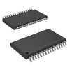
SN761683DAR
Texas Instruments
IC VIDEO TUNER 32TSSOP
AD664AD-UNI
Analog Devices Inc.
IC DAC 12BIT V-OUT 28CDIP
VI-2WM-EX
Vicor Corporation
DC DC CONVERTER 10V 75W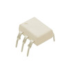
CNY17F-3M
Everlight Electronics Co Ltd
OPTOISOLTR 5KV TRANSISTOR 6-DIP -

06033C104MAT2A
AVX Corporation
CAP CER 0.1UF 25V X7R 0603
LPV358DGKRG4
Texas Instruments
IC OPAMP GP 2 CIRCUIT 8VSSOP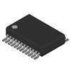
PCM3501E
Burr Brown
PCM3501 LOW VOLTAGE, LOW POWER,
EMK105BJ104KV-F
Taiyo Yuden
CAP CER 0.1UF 16V X5R 0402
MUN5331DW1T1G
onsemi
TRANS PREBIAS 1NPN 1PNP 50V SC88
BCR148WH6327
Infineon Technologies
BIPOLAR DIGITAL TRANSISTOR
TCR3DF33,LM
Toshiba Semiconductor and Storage
IC REG LINEAR 3.3V 300MA SMV
MBR20150CT
Yangzhou Yangjie Electronic Technology Co.,Ltd
SCHOTTKY DIODE 150V 20A TO-220AB
PCD1R5-24-1212
TDK-Lambda Americas Inc
DC DC CONVERTER +/-12V 1.44W
APT8030LVRG
Microchip Technology
MOSFET N-CH 800V 27A TO264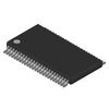
CY74FCT16244ATPACT
Cypress Semiconductor Corp
IC BUFF NON-INVERT 5.5V 48TSSOP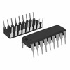
MIC2981/82BN
Microchip Technology
IC PWR DRIVER BIPOLAR 1:1 18DIP
TLC7524CNSR
Texas Instruments
IC DAC 8BIT A-OUT 16SO
2SC3735-T1B-A
Renesas Electronics America Inc
SMALL SIGNAL BIPOLAR TRANSTR NPN
FDS6673BZ
onsemi
MOSFET P-CH 30V 14.5A 8SOIC
EL5151IWZ-T7A
Renesas Electronics America Inc
IC OPAMP VFB 1 CIRCUIT SOT23-5
LTC2631ITS8-LM8#TRMPBF
Linear Technology
IC DAC 8BIT V-OUT TSOT23-8
DBS400B15
Cosel USA, Inc.
DC DC CONVERTER 15V 405W -

TDE3247FPT
STMicroelectronics
IC PWR DRIVER BIPOLAR 1:1 14SO
TLV1543CFN
Texas Instruments
IC ADC 10BIT SAR 20PLCC
AQV251AX
Panasonic Electric Works
SSR RELAY SPST-NO 500MA 0-40V
LT3574IMS#PBF
Analog Devices Inc.
IC REG FLYBACK 650MA 16MSOP
INA125PAG4
Texas Instruments
IC INST AMP 1 CIRCUIT 16DIP
BU2630FV-E2
Rohm Semiconductor
IC PLL FREQ SYNTH 16SSOP
INA2134UA/2K5
Texas Instruments
IC AUDIO DIFF LINE RCVR 14SOIC
02016D225MAT2A
AVX Corporation
CAP CER 2.2UF 6.3V X5R 0201
EP3C10U256C6N
Intel
IC FPGA 182 I/O 256UBGA
C3216CH2E332J085AA
TDK Corporation
CAP CER 3300PF 250V CH 1206
06035A331KAT4A
KYOCERA AVX
CAP CER 330PF 50V C0G/NP0 0603
C3216CH2J561J085AA
TDK Corporation
CAP CER 560PF 630V CH 1206
PMV55ENEAR
Nexperia USA Inc.
MOSFET N-CH 60V 3.1A TO236AB
SDA02H0SBD
C&K
SWITCH SLIDE DIP SPST 25MA 24V
FQA16N50
onsemi
MOSFET N-CH 500V 16A TO3P
OPA837IDCKR
Texas Instruments
IC OPAMP VFB 1 CIRCUIT SC70-5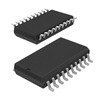
74HC574D,653
Nexperia USA Inc.
IC FF D-TYPE SNGL 8BIT 20SO
MLG0603P2N8BT000
TDK Corporation
FIXED IND 2.8NH 500MA 200MOHM SM