AT89S52-24PU Microcontroller: Alternatives, Pinout, and Datasheet
This article explores the AT89S52-24PU microcontroller, highlighting its characteristics, practical uses, and how it efficiently handles power and performance in demanding applications. Renowned for its 8K bytes of Flash memory and low power consumption, this device is ideal looking to balance energy efficiency with robust functionality in battery-powered devices.Catalog
What is the AT89S52-24PU?
The AT89S52-24PU microcontroller is a highly flexible device that integrates an 8-bit CPU with programmable Flash memory on a single chip. By harnessing Atmel's advanced nonvolatile memory technology, this microcontroller maintains compatibility with the esteemed 80C51 instruction set. Its on-chip reprogrammable Flash caters to the diverse needs of various embedded control systems in a manner that is both efficient and cost-effective. The microcontroller features 8K of Flash and 256 bytes of RAM, providing ample capacity for intricate programming and catering to applications demanding complex data processing. The inclusion of 32 general-purpose I/O lines offers the versatility to connect a wide range of peripherals.
With three 16-bit timer/counters, the AT89S52-24PU supports precise time-based functions, which are invaluable for data processing and control settings. The dual data pointers enhance data handling efficiency, supporting rapid data transfer scenarios effectively. The Watchdog timer adds a layer of reliability by resetting the system during software irregularities, a feature cherished by sectors prioritizing long-term system integrity. The microcontroller's capacity for static operation at various frequencies aids in balancing performance with power consumption. The availability of power-saving modes, including Idle and Power-down, underscores its appropriateness for battery-operated applications, ensuring memory content retention during power-down phases. These features address energy efficiency concerns, as evidenced by its adoption in portable and remotely-operated devices.
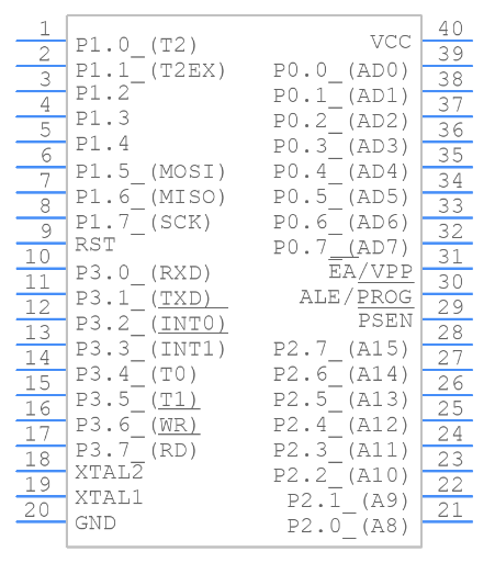
AT89S52-24PU Pin Configuration

|
Pin No |
Pin Name |
Description |
|
1-8 |
Port 1 |
Interface 1 has internal pull-ups and is an 8-bit
bidirectional I/O port. Four TTL inputs can be sink/source in the Port 1
output buffers. When 1s are written to Port 1 pins, the internal pull-ups
pull them high, allowing them to be used as inputs. Because of the internal
pull-ups, Port 1 pins that are externally pushed low will source current
(IIL) as inputs. In addition, as shown in the table, P1.0 and P1.1 can be set
to be the timer/counter 2 external count input (P1.0/T2) and the
timer/counter 2 trigger input (P1.1/T2EX), respectively. During Flash
programming and verification, Port 1 also receives the low-order address
bytes. |
|
9 |
RST |
Input should be reset. While the oscillator is
functioning, a high on this pin for two machine cycles resets the device.
After the Watchdog has timed out, this pin goes high for 98 oscillator
periods. This feature can be disabled using the DISRTO bit in SFR AUXR
(address 8EH). The RESET HIGH out capability is enabled by default in bit
DISRTO. |
|
10-17 |
Port 3 |
Port 3 is an internal pull-up 8-bit bidirectional I/O
port. Four TTL inputs can be sunk or sourced using the Port 3 output buffers.
When 1s are written to Port 3 pins, the internal pull-ups pull them high,
allowing them to be used as inputs. Because of the pull-ups, Port 3 pins that
are externally pulled low will source current (IIL) as inputs. For Flash
programming and verification, Port 3 receives some control signals. As stated
in the chart below, Port 3 also supports the functions of numerous AT89S52
special features. |
|
18 |
XTAL2 |
Output from the inverting oscillator amplifier. |
|
19 |
XTAL1 |
Input to the inverting oscillator amplifier and input to
the internal clock operating circuit. |
|
20 |
GND |
Ground. |
|
21-28 |
Port 2 |
Port 2 is an internal pull-up 8-bit bidirectional I/O
port. Four TTL inputs can be sink/source in the Port 2 output buffers. When
1s are written to Port 2 pins, the internal pull-ups pull them high, allowing
them to be used as inputs. Because of the internal pull-ups, Port 2 pins that
are externally pushed low will source current (IIL) as inputs. During fetches
from external program memory and accesses to external data memory that use
16-bit addresses (MOVX @ DPTR), Port 2 emits the high-order address byte.
When transmitting 1s, Port 2 uses powerful internal pull-ups in this
application. Port 2 emits the contents of the P2 Special Function Register
during 8-bit address accesses to external data memory (MOVX @ RI). During
Flash programming and verification, Port 2 additionally gets the high-order
address bits and various control signals. |
|
29 |
PSEN |
The read strobe to external program memory is called
Program Store Enable (PSEN). PSEN is activated twice each machine cycle when
the AT89S52 is running code from external program memory, with two PSEN
activations ignored during each access to external data memory. |
|
30 |
ALE/PROG |
The Address Latch Enable (ALE) output pulse is used to
latch the low byte of the address during external memory accesses. During
Flash programming, this pin also serves as the program pulse input (PROG).
ALE is released at a steady rate of 1/6 the oscillator frequency in normal
operation and can be used for external timing or clocking. However, during
each access to external data memory, one ALE pulse is skipped. Setting bit 0
of SFR location 8EH to 0 disables ALE functioning if desired. ALE is only active
when the bit is set via a MOVX or MOVC instruction. Otherwise, the pin is
lifted high but weakly. If the microcontroller is in external execution mode,
setting the ALE-disable bit has no effect. |
|
31 |
EA/VPP |
External Access is turned on. To enable the device to
fetch code from external program memory regions beginning at 0000H and ending
at FFFFH, EA must be connected to GND. If lock bit 1 is coded, however, EA
will be internally latched on reset. For internal program executions, EA
should be tied to VCC. During Flash programming, this pin additionally
receives the 12-volt programming enable voltage (VPP). |
|
32-39 |
Port 0 |
Interface 0 is a bidirectional 8-bit open drain I/O port.
Each pin can sink eight TTL inputs as an output port. The pins on port 0 can
be used as high-impedance inputs when 1s are written to them. During accesses
to external program and data memory, Port 0 can also be set as the
multiplexed low-order address/data bus. P0 features internal pull-ups in this
mode. During Flash programming, Port 0 also gets the code bytes and outputs
them during program verification. During program verification, external pull-ups
are required. |
|
40 |
VCC |
Supply voltage. |
AT89S52-24PU Symbol, Footprint, and CAD Model
AT89S52-24PU Symbol
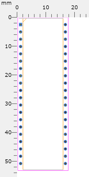
AT89S52-24PU Footprint
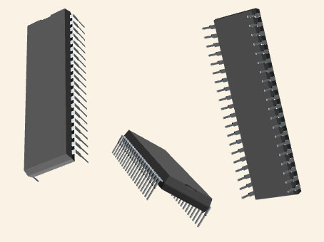
AT89S52-24PU CAD Model
Features of the AT89S52-24PU
• MCS®-51 Standard Compliance: Fully compatible with the MCS®-51 standard, ensuring robust and reliable performance.
• 8K ISP Flash Memory: Stores large programs. Supports up to 10,000 write/erase cycles, ideal for long-term applications.
• Wide Operating Voltage (4V–5.5V): Adapts to various power supply environments.
• High-Speed Operation: Handles static conditions up to 33 MHz, balancing energy efficiency with performance needs.
• Enhanced Security: Memory lock features protect intellectual property. Prevents unauthorized access or modifications.
• Flexible I/O and Timer Functions: Easy integration with sensors and devices. Precise control for time applications requiring accurate timing.
• Dual Data Pointers: Boosts efficiency in data-heavy tasks like signal processing and communication. Simplifies data stream handling.
• Energy-Saving Modes: Idle and Power-down modes reduce energy consumption. Optimized for portable devices and sustainable designs.
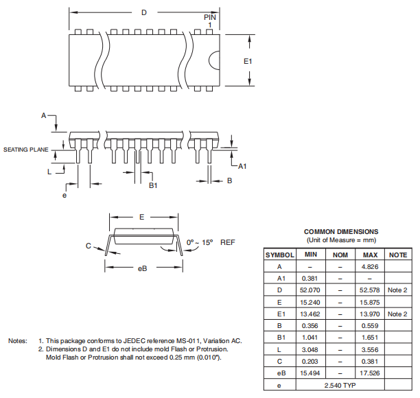
AT89S52-24PU Technical Specifications
|
Type |
Parameter |
|
Factory Lead Time |
7 Weeks |
|
Mount |
Through Hole |
|
Package / Case |
40-DIP (0.600, 15.24mm) |
|
Number of I/Os |
32 |
|
Operating Temperature |
-40°C~85°C TA |
|
Series |
89S |
|
JESD-609 Code |
e3 |
|
Part Status |
Active |
|
Number of Terminations |
40 |
|
Supply Voltage |
5V |
|
Frequency |
33MHz |
|
Operating Supply Voltage |
5V |
|
Interface |
UART |
|
Contact Plating |
Tin |
|
Mounting Type |
Through Hole |
|
Number of Pins |
40 |
|
Watchdog Timers |
Yes |
|
Packaging |
Tube |
|
Published |
1997 |
|
Pbfree Code |
yes |
|
Moisture Sensitivity Level (MSL) |
1 (Unlimited) |
|
Terminal Position |
DUAL |
|
Terminal Pitch |
2.54mm |
|
Base Part Number |
AT89S52 |
|
Power Supplies |
5V |
|
Memory Size |
8kB |
|
Speed |
24 MHz |
|
Voltage - Supply (Vcc/Vdd) |
4V~5.5V |
|
Number of Bits |
8 |
|
Peripherals |
WDT |
|
Core Size |
8-Bit |
|
Connectivity |
UART/USART |
|
Access Time |
24 µs |
|
DMA Channels |
NO |
|
PWM Channels |
NO |
|
Number of Timers/Counters |
3 |
|
Number of UART Channels |
1 |
|
Length |
52.58mm |
|
REACH SVHC |
No SVHC |
|
RoHS Status |
ROHS3 Compliant |
|
Oscillator Type |
Internal |
|
RAM Size |
256 x 8 |
|
uPs/uCs/Peripheral ICs Type |
MICROCONTROLLER |
|
Core Processor |
8051 |
|
Program Memory Type |
FLASH |
|
Program Memory Size |
8KB 8K x 8 |
|
Bit Size |
8 |
|
Has ADC |
NO |
|
Data Bus Width |
8b |
|
DAC Channels |
NO |
|
Address Bus Width |
8b |
|
Height |
4.826mm |
|
Width |
13.97mm |
|
Radiation Hardening |
NO |
|
Lead Free |
Lead Free |
AT89S52-24PU Similar Parts
The three components listed to the right are similar in specifications to those of Microchip Technology AT89S52-24PU.
|
Part Number |
Manufacturer |
Package / Case |
Number of Pins |
Data Bus Width |
Number of I/O |
Interface |
Memory Size |
Supply Voltage |
Peripherals |
|
AT89S52-24PU |
Microchip Technology |
40-DIP (0.600, 15.24mm) |
40 |
8 b |
32 |
UART |
8 kB |
5 V |
WDT |
|
AT89C55WD-24PU |
Microchip Technology |
40-DIP (0.600, 15.24mm) |
40 |
8 b |
32 |
SPI, UART, USART |
32 kB |
5 V |
WDT |
|
AT89S51-24PU |
Microchip Technology |
40-DIP (0.600, 15.24mm) |
40 |
8 b |
32 |
UART, USART |
4 kB |
5 V |
WDT |
|
AT89C51RC-24PU |
Microchip Technology |
40-DIP (0.600, 15.24mm) |
40 |
8 b |
32 |
UART, USART |
20 kB |
- |
WDT |
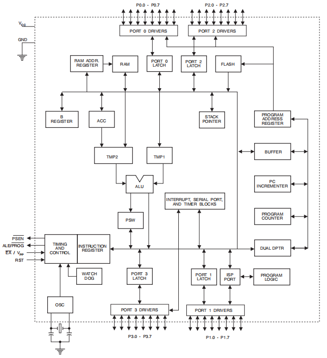
Functional Block Diagram of the AT89S52-24PU
The diagram below illustrates the functional block structure of the AT89S52-24PU.
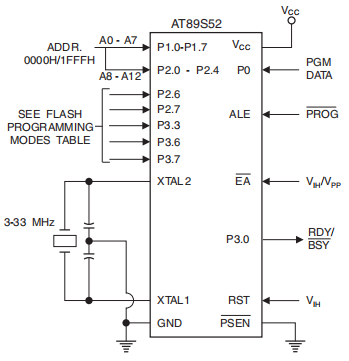
Programming the Flash Memory (Parallel Mode)
The figure below illustrates the process of programming the Flash memory of the AT89S52-24PU in parallel mode.
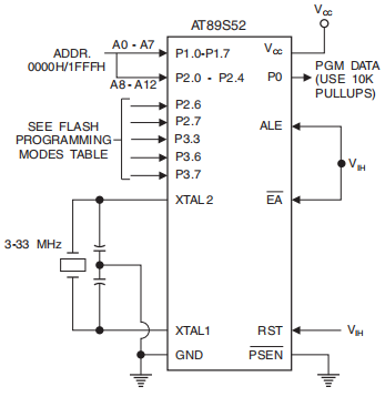
Verifying the Flash Memory (Parallel Mode)
The figure below demonstrates the process of verifying the flash memory in parallel mode for the AT89S52-24PU.
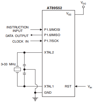
Flash Memory Serial Downloading
The figure below illustrates the Serial Downloading process for the AT89S52-24PU Flash Memory.
Alternatives of the AT89S52-24PU
|
Part Number |
Description |
Manufacturer |
|
AT87F52-24PC |
Microcontroller, 8-Bit, FLASH, 8051 CPU, 24MHz, CMOS,
PDIP40, 0.600 INCH, PLASTIC, DIP-40 |
Atmel Corporation |
|
AT87F52-24PI |
Microcontroller, 8-Bit, FLASH, 8051 CPU, 24MHz, CMOS,
PDIP40, 0.600 INCH, PLASTIC, DIP-40 |
Atmel Corporation |
|
AT87F52-24PL |
Microcontroller, 8-Bit, FLASH, 24MHz, CMOS, PDIP40, 0.600
INCH, PLASTIC, DIP-40 |
Atmel Corporation |
Applications of the AT89S52-24PU
• Healthcare Monitoring: Enhances precision in medical monitoring devices.
• Automotive Safety: Integrates features like adaptive cruise control and lane assistance.
• DIY Electronics: Enables hobbyists to create custom devices.
• Consumer Electronics: Produces multifunctional and intuitive products.
• Smart Homes and Cities: Improves device communication for better energy management and convenience.
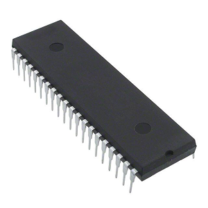
Package for AT89S52-24PU
AT89S52-24PU Manufacturer Information
Microchip Technology Inc., with its headquarters nestled in Chandler, Arizona, plays a role in the microcontroller and semiconductor industry. The company is distinguished by its steadfast dedication to pioneering advancements and maintaining high standards through product lines recognized for their reliability, which bolster development efficiency and economic prudence. By carefully refining its design and manufacturing processes, Microchip not only meets but surpasses industry benchmarks, nurturing a setting that encourages ongoing enhancement and system refinement. Microchip Technology Inc. is much more than a provider of microcontrollers and semiconductors; it actively molds the landscape in which these technologies are developed and utilized. Its strategic emphasis on efficiency, cost management, and quality control places it at the vanguard of the industry.
Datasheet PDF
AT89S52-24PU Datasheets:
Copper Bonding Wire 17/Oct/2013.pdf
AT89C55WD-24PU Datasheets:
Cylindrical Battery Holders.pdf
Transfer to Microchip/Label/Pkg 5/Sep/2016.pdf
Transfer to Microchip/Label/Pkg 5/Sep/2016.pdf
Cylindrical Battery Holders.pdf
AT89S51-24PU Datasheets:
Cylindrical Battery Holders.pdf
Copper Bonding Wire 17/Oct/2013.pdf
AT89C51RC-24PU Datasheets:
MBB/Label Chgs 16/Nov/2018.pdf
About us
ALLELCO LIMITED
Read more
Quick inquiry
Please send an inquiry, we will respond immediately.
Frequently Asked Questions [FAQ]
1. How do AT89S51 and AT89S52 diverge?
The primary difference centers on their Flash memory size: AT89S51 is equipped with 4K while AT89S52 expands this to 8K. This expansion supports more sophisticated applications and the storage of extensive code bases, aligning with diverse needs in embedded systems development.
2. What are the applications of AT89S52?
AT89S52 is employed in several embedded control tasks, often valued for energy efficiency and reliable performance. Its versatility frequently makes it a favored option in projects aiming for cost-effectiveness while maintaining functionality, aligning with balance innovation with financial considerations.
3. Can you elaborate on AT89S52-24PU?
This is an 8-bit CMOS microcontroller, known for merging computational and memory capabilities into a compact unit. These qualities are enticing in streamlined design processes where efficiency and space are important.
4. Why is the AT89S52-24PU reprogrammable?
On-chip Flash memory allows reprogramming, offering adaptability for software updates and iterative development. This feature complements a modern development perspective where continuous improvements are not only possible but welcomed.
5. What configuration integrates an 8-bit CPU with Flash memory?
The AT89S52-24PU exemplifies this combination, where an 8-bit CPU harmonizes with Flash memory. This integration delivers effective processing and storage for applications demanding robust operations without excess.
6. What size of Flash memory does it possess?
It comprises 8K bytes of Flash, enabling the management of program data. This expansiveness makes it suitable for challenging tasks where limited memory could pose obstacles.
7. How does AT89S52 handle low frequency operation?
Static logic is included, allowing operation at low frequencies with efficiency. This characteristic is use in scenarios demanding minimal power use, enhancing both longevity and sustainability in electronics.
8. When does the CPU become inactive?
Idle Mode renders the CPU inactive, achieving energy savings while maintaining microcontroller functions. This strategic design minimizes energy use during periods of less intensive processing.
9. Which mode maintains RAM integrity?
RAM contents remain intact during power-down mode, enabling data preservation despite reduced power consumption. This functionality is good in conditions necessitating data retention alongside minimal energy usage, typical in battery-powered devices.
KSZ9031RNXIA Gigabit Ethernet Transceiver: Pinout, Alternatives, and Datasheet
on November 22th
Exploring the FOD3180 Optocoupler
on November 22th
Popular Posts
-

Complex Instruction Set Computers: How They Changed Computing?
on April 18th 147749
-

USB-C Pinout and Features
on April 18th 111909
-

Using Xilinx Unified Simulation Primitives: A Comprehensive Guide to FPGA Design and Simulation
on April 18th 111349
-

Power Supply Voltages in Electronics: Meaning of VCC, VDD, VEE, VSS, and GND
on April 18th 83714
-

RJ45 Connector Guide: Pinout, Wiring, Cable Types, and Uses
on January 1th 79502
-

The Ultimate Guide to Wire Color Codes in Modern Electrical Systems
The way our electrical systems use colors isn’t just for looks. Each wire color now indicates a specific function, making it easier to identify and handle electrical components correctly during ins...on January 1th 66871
-

Quality (Q) Factor: Equations and Applications
The quality factor, or 'Q', is important when checking how well inductors and resonators work in electronic systems that use radio frequencies (RF). 'Q' measures how well a circuit minimizes energy...on January 1th 63005
-

Purge Valve Guide: Function, Symptoms, Testing, and Replacement for Optimal Engine Performance
The purge valve is a key part of a car’s system that helps keep the air clean by managing fuel vapors before they can escape into the atmosphere. This not only helps the environment by reducing pol...on January 1th 62947
-

Achieving Peak Performance with the Maximum Power Transfer Theorem
The Maximum Power Transfer Theorem explains how energy from a source, such as a battery or generator, flows to a connected load. It shows the exact condition where the load receives the most power....on January 1th 54077
-

A23 Battery Specifications and Compatibility
The A23 battery is a small, cylinder-shaped battery with high voltage. Also called 23A, 23AE, or MN21, it runs at 12 volts and much higher than AA or AAA batteries. Its special design make...on January 1th 52089
HOT Part Number
-

BD9B100MUV-E2
Rohm Semiconductor
IC REG BUCK ADJ 1A 16VQFN
UPD70F3539AF5A9-PN7-Q-A
Renesas Electronics America Inc
IC MICROCONTROLLER
18081A621JAT2A
KYOCERA AVX
CAP CER 620PF 100V NP0 1808
FDN340P
onsemi
MOSFET P-CH 20V 2A SUPERSOT3
70231-101
Amphenol ICC (FCI)
CONN RCPT BLADE PWR 8POS EDGE MT
MPSW42RLRAG
onsemi
TRANS NPN 300V 0.5A TO92
MC7824BT
onsemi
IC REG LINEAR 24V 1A TO220AB
AD8009ARZ-REEL
Analog Devices Inc.
IC OPAMP CFA 1 CIRCUIT 8SOIC
LT1815CS5#TRPBF
Analog Devices Inc.
IC OPAMP VFB 1 CIRCUIT TSOT23-5
DG411DYZ
Renesas Electronics America Inc
IC SWITCH SPST-NCX4 35OHM 16SOIC
VFT2060C-M3/4W
Vishay General Semiconductor - Diodes Division
DIODE SCHOTTKY 20A 60V ITO-220AB
TSX562AIYST
STMicroelectronics
IC CMOS 2 CIRCUIT 8MINISO
MR256D08BMA45
Everspin Technologies Inc.
IC RAM 256KBIT PARALLEL 48FBGA
VSC3312YYP-01
Microchip Technology
IC SWITCH 16X16 6.5GBPS 196FCBGA
XC68HC908GP20CFB
Motorola
TSG 8BIT20K FLASH
CSR8811A08-ICXR-R
Qualcomm
IC RF TXRX+MCU BLUETOOTH
MPSW05
onsemi
TRANS NPN 60V 0.5A TO92
1N4055R
Solid State Inc.
DIODE GEN PURP REV 900V 275A DO9 -

ASX342ATSC00XPED0-DP
onsemi
IMAGE SENSOR VGA 1/4 CIS SOC
0433.125NR
Littelfuse Inc.
FUSE BOARD MNT 125MA 125VAC/VDC
1SMA5941BT3G
onsemi
DIODE ZENER 47V 1.5W SMA
DCP010512BP-U/700
Texas Instruments
DC DC CONVERTER 12V 1W
1-1734344-1
TE Connectivity AMP Connectors
CONN D-SUB HD RCPT 15P R/A SLDR
KSD1621STF
onsemi
TRANS NPN 25V 2A SOT89-3
BQ24161RGET
Texas Instruments
IC BATT CHG LI-ION 1CELL 24VQFN
BTA26-600BW
STMicroelectronics
TRIAC ALTERNISTOR 600V 25A TOP3
NCP1239DD65R2G
onsemi
IC OFFLINE SWITCH FLYBACK 7SOIC
TMS320TCI6482BZTZA
Texas Instruments
TMS320 - DIGITAL SIGNAL PROCESSO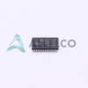
BQ20Z90DBTR-V150
Texas Instruments
IC GAS GAUGE LI-ION 30TSSOP
PCMB104T-1R0MT
Susumu
FIXED IND 1UH 18A 3.3 MOHM SMD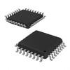
CY29942AXCT
Infineon Technologies
IC CLK BUFFER 1:18 200MHZ 32TQFP
CC0402KRX7R9BB561
YAGEO
CAP CER 560PF 50V X7R 0402
STPS20M60SG-TR
STMicroelectronics
DIODE SCHOTTKY 60V 20A D2PAK
AT25010N-10SC-2.7
Microchip Technology
IC EEPROM 1KBIT SPI 3MHZ 8SOIC
04023A1R0CAT4A
KYOCERA AVX
CAP CER 1PF 25V C0G/NP0 0402
ISL6327IRZ
Intersil
SWITCHING CONTROLLER, VOLTAGE-MO -

LQW18AN75NG0ZD
Murata Electronics
FIXED IND
DFA100BA160
SanRex Corporation
DIODE MODULE 1600V 100A
BAR46AFILM
STMicroelectronics
DIODE ARRAY SCHOTTKY 100V SOT23
MAX825SEUK
Analog Devices Inc./Maxim Integrated
IC SUPERVISOR MPU
MMST2222A-7-F
Diodes Incorporated
TRANS NPN 40V 0.6A SOT323
FODM8801AR2
onsemi
OPTOISO 3.75KV TRANS 4-MINI-FLAT
FJV1845FMTF
Fairchild Semiconductor
SMALL SIGNAL BIPOLAR TRANSISTOR,
EVK105RH5R1JW-F
Taiyo Yuden
CAP CER 5.1PF 16V R2H 0402
6651170-3
TE Connectivity AMP Connectors
CONN EDGE DUAL FMALE 4POS 0.508
KSZ8893FQLI-FX
Microchip Technology
IC SWITCH ETH 3PORT 128QFP
170M6340
Eaton - Bussmann Electrical Division
FUSE SQUARE 400A 1.3KVAC RECT
BCM20741A2KFB1G
Broadcom Limited
SINGLE-CHIP BLUETOOTH
MAX3443EASA+
Analog Devices Inc./Maxim Integrated
IC TRANSCEIVER HALF 1/1 8SOIC
GRM0335C1H9R3DA01D
Murata Electronics
CAP CER 9.3PF 50V C0G/NP0 0201
TNY175PN
Power Integrations
11.5 W (85-265 VAC) 15 W (230 VA
742700726
Würth Elektronik
FERRITE CORE 278 OHM SOLID 4MM
DM74S20N
onsemi
IC GATE NAND 2CH 4-INP 14DIP
P4SMA56CA-E3/61
Vishay General Semiconductor - Diodes Division
TVS DIODE 47.8VWM 77VC DO214AC