Analog-to-Digital Converter (ADC): Working Principle, Types, Specifications, and Applications
In this article, you’ll learn what an Analog-to-Digital Converter (ADC) is and how it turns signals into digital data that your devices can understand. You’ll see how the conversion process works, what key specifications you should pay attention to, and why they matter. You’ll also explore the different types of ADCs and how each one operates. By the end, you’ll understand where ADCs are used and how they compare to DACs.Catalog
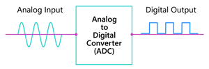
Figure 1. Analog-to-Digital Converter (ADC) Diagram
What is an Analog-to-Digital Converter?
An Analog-to-Digital Converter (ADC) is a device that converts a continuously varying analog signal such as voltage, sound, light, or temperature into a digital value that a microcontroller or computer can process. In the figure, the smooth wave on the left represents the analog input, which is a continuous signal that changes over time. As this signal enters the ADC in the center, it is converted into a series of discrete digital values. The block-like pattern on the right shows the digital output, which is now in a form that digital systems can read and interpret. This simple illustration demonstrates the main purpose of an ADC: transforming analog signals into clear, usable digital data for electronic devices and embedded systems.
Working Principle of Analog-to-Digital Converter
An Analog-to-Digital Converter (ADC) works by turning a changing analog signal into a digital value that a computer or microcontroller can understand. The process has three main parts: sampling, quantization, and encoding.
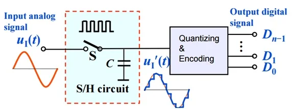
Figure 2. Working Principle of an Analog-to-Digital Converter (ADC)
In the figure above, the analog input signal enters the sample-and-hold (S/H) circuit, where the ADC first performs sampling. This step captures the signal at regular time intervals, creating a series of discrete snapshots that freeze the changing waveform so it can be processed. After sampling, the signal moves into the quantizing and encoding block, where quantization takes place. Here, each sampled point is approximated to the nearest available digital level based on the ADC’s resolution, which determines how precisely the analog value can be represented. Finally, the ADC performs encoding, converting the quantized values into a binary output that digital circuits, microcontrollers, or processors can understand.
Analog-to-Digital Converter Specifications
|
Type |
Specifications |
|
Resolution
(bits) |
8-bit, 10-bit,
12-bit, 16-bit, 24-bit |
|
Sampling
Rate (SPS / Hz) |
10 kS/s to 1
MS/s (SAR), up to 100 MS/s (pipeline) |
|
Input
Voltage Range |
0–5 V, 0–3.3 V,
±2.5 V |
|
Reference
Voltage (Vref) |
1.024 V, 2.048
V, 4.096 V |
|
SNR
(Signal-to-Noise Ratio) |
60 dB (10-bit),
74 dB (12-bit), 98 dB (16-bit) |
|
ENOB
(Effective Number of Bits) |
9.5 bits, 11.8
bits, 15.5 bits |
|
INL
(Integral Nonlinearity) |
±0.5 LSB, ±1
LSB |
|
DNL
(Differential Nonlinearity) |
±0.3 LSB, ±1
LSB |
|
Conversion
Time |
1 µs (SAR), 20
ns (pipeline) |
|
Power Consumption |
2 mW to 50 mW |
|
Input
Impedance |
1 kΩ to >1
MΩ |
|
Offset Error |
±1 mV, ±2 mV |
|
Gain Error |
±0.05%, ±0.1% |
|
Aperture
Jitter |
1 ps to 50 ps |
|
Communication
Interface |
SPI, I²C,
Parallel, LVDS |
Types of Analog-to-Digital Converters
Successive Approximation Register (SAR) ADC
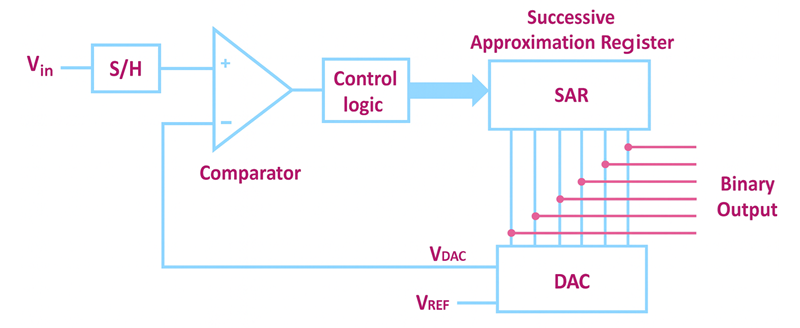
Figure 3. Successive Approximation Register (SAR) ADC Diagram
A Successive Approximation Register (SAR) ADC converts an analog signal into a digital value by comparing the input voltage to the output of an internal DAC and adjusting the result one bit at a time. This method allows the SAR ADC to quickly narrow down the closest digital representation of the input signal with good accuracy. In the figure above, the process begins with the input voltage passing through the sample-and-hold circuit, which captures the signal for conversion. The comparator then checks whether the input voltage is higher or lower than the DAC output, and the control logic sends this information to the SAR block, which updates each bit in sequence. As the SAR refines the value, the DAC generates new comparison voltages until the final digital output is reached.
Flash ADC (Parallel ADC)

Figure 4. Flash ADC (Parallel ADC) Diagram
A Flash ADC, also known as a Parallel ADC, converts an analog signal into a digital value almost instantly by using a large number of comparators operating at the same time. This architecture makes it the fastest type of ADC. In the figure above, the input voltage is fed into a resistor ladder that creates a series of reference voltage levels. Each comparator compares the input voltage to one of these reference points and switches its output based on whether the input is higher or lower. All comparator outputs are then sent to a priority encoder, which converts these signals into the final binary output. This parallel operation makes a Flash ADC extremely fast, but it also uses more power and usually provides lower resolution than other ADC types.
Sigma-Delta (ΔΣ) ADC

Figure 5. Sigma-Delta (ΔΣ) ADC Diagram
A Sigma-Delta (ΔΣ) ADC converts an analog signal into a high-resolution digital output by oversampling the input and using noise-shaping techniques to push unwanted noise out of the useful frequency range. This approach allows the converter to achieve extremely accurate measurements, making it ideal for audio devices, precision instruments, and low-frequency sensor systems. In the figure above, the process begins with the analog input entering the sigma-delta modulator, where the signal is integrated and compared using a 1-bit ADC. The comparator generates a rapid stream of 1-bit data, while the feedback loop and 1-bit DAC continuously adjust the system to shape and reduce noise. This high-speed bitstream then passes through a digital filter and decimator, which averages and converts it into a final multi-bit digital output.
Dual-Slope ADC
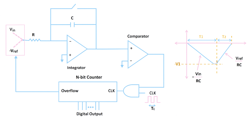
Figure 6. Dual-Slope ADC Diagram
A Dual-Slope ADC converts an analog signal into a digital value by integrating the input voltage over a fixed time and then measuring how long it takes to discharge using a precise reference voltage. This method naturally filters out noise and provides very stable measurements, which is why dual-slope ADCs are widely used in digital multimeters and other precision instrumentation. In the figure above, the input voltage is first applied to the integrator through a resistor, causing the integrator’s output to ramp up over a set period. After this integration phase, the circuit switches to a reference voltage of opposite polarity, and the integrator ramps back down toward zero. A counter measures the time required for this de-integration, and that time is directly proportional to the input voltage.
Pipeline ADC
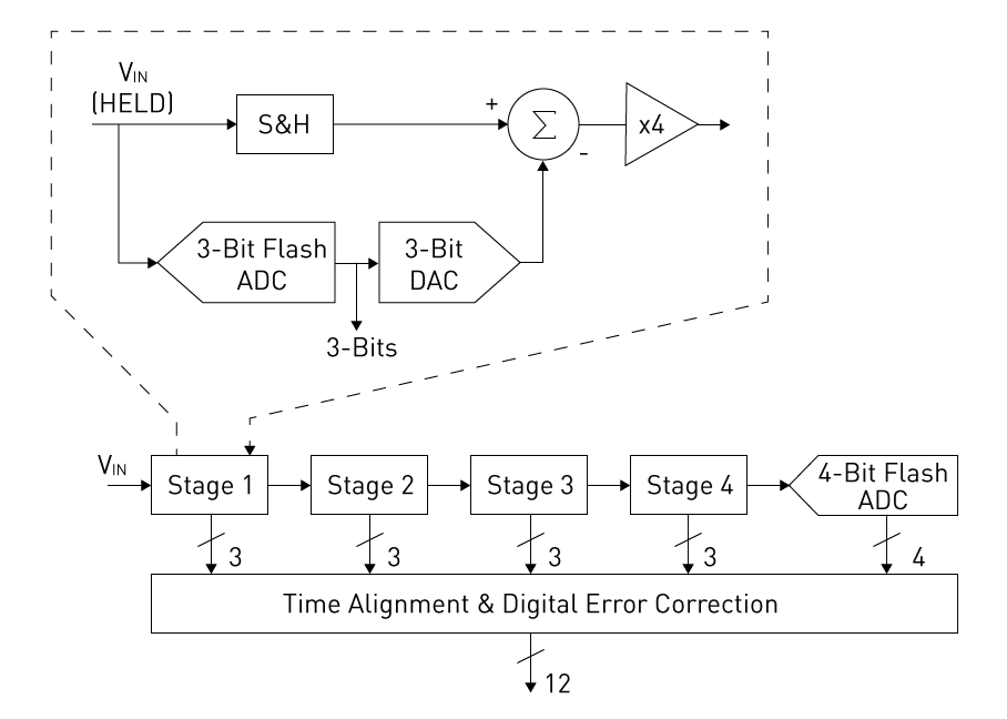
Figure 7. Pipeline ADC Diagram
A Pipeline ADC converts an analog signal into a digital value by passing it through a series of stages, with each stage resolving a few bits before passing the remaining error to the next. This staged approach allows pipeline ADCs to achieve both high speed and good resolution, making them ideal for video processing, high-speed data acquisition, and RF communication systems. In the figure above, the input signal enters the first conversion stage, where a small flash ADC and DAC work together to generate a partial digital output and an amplified residue signal. This residue is then sent to the next stage, and the process repeats as the signal moves through multiple stages. At the end of the pipeline, all partial outputs are combined through time alignment and digital error correction to produce the final high-resolution digital result.
Integrating ADC
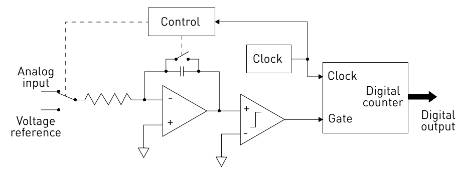
Figure 8. Integrating ADC Diagram
An Integrating ADC converts an analog signal into a digital output by measuring how the input voltage changes over time within an integrator circuit. This method naturally filters out noise and produces stable, highly reliable readings, making integrating ADCs ideal for scientific instruments, monitoring systems, and other applications where accuracy matters more than speed. In the figure above, the analog input is applied to an integrator through a resistor, causing the integrator’s output to ramp upward or downward depending on the input voltage. A comparator monitors this ramp, and a digital counter (driven by a clock) measures how long it takes for the integrator’s output to reach a reference level. The control circuitry then manages switching between the input voltage and the reference voltage, ensuring consistent operation. The time recorded by the counter is directly proportional to the input signal, and this value becomes the digital output.
ADC Challenges and Limitations
• Limited accuracy caused by quantization error
• Easily affected by electrical noise and interference
• Nonlinearity issues that reduce measurement precision
• Higher resolution increases complexity and noise sensitivity
• Incorrect sampling rate can lead to aliasing problems
• Trade-off between speed and accuracy in many designs
• Requires careful analog signal conditioning for best performance
ADC vs. DAC
|
Specification |
ADC
(Analog-to-Digital Converter) |
DAC
(Digital-to-Analog Converter) |
|
Function |
Converts analog
signals into digital signals |
Converts
digital signals into analog signals |
|
Input Type |
Analog
voltage/current |
Digital code
(binary) |
|
Output Type |
Digital binary
value |
Analog
voltage/current |
|
Common
Resolution |
8, 10, 12, 16,
24 bits |
8, 10, 12, 16
bits |
|
Sampling
Rate |
From kSPS to
hundreds of MSPS |
From kSPS to
tens of MSPS |
|
Conversion
Time |
Slower (μs–ns
range) |
Faster (ns–μs
range) |
|
Accuracy |
Limited by
quantization error |
Higher
linearity and smooth output |
|
Linearity
Error |
±1 to ±4 LSB
typical |
±0.5 to ±2 LSB
typical |
|
Noise Level |
Higher
(affected by input signal) |
Lower (cleaner
analog output) |
|
Complexity |
More complex
internal architecture |
Simpler
architecture |
|
Power
Consumption |
Higher in
high-speed models |
Generally lower |
|
Common Types |
SAR, Flash,
Sigma-Delta, Pipeline |
R-2R, Weighted
Resistor, Sigma-Delta |
|
Applications |
Sensors,
measurement, data acquisition |
Audio output,
signal generation |
|
Required
Reference Voltage |
Yes, for
accurate digital output |
Yes, for stable
analog output |
Applications of Analog-to-Digital Converter
Sensor Data Acquisition
Sensors such as temperature, pressure, and light produce analog signals that must be converted into digital form. ADCs make this conversion so microcontrollers and computers can read and process the data. This allows accurate monitoring and automation in countless electronic systems.
Audio Recording and Processing
Microphones generate analog sound waves that ADCs convert into digital signals. This digital conversion allows the audio to be stored, edited, or streamed. Without ADCs, modern music production, voice recording, and communication systems would not be possible.
Imaging and Digital Cameras
Camera sensors detect light as analog signals, which ADCs convert into digital pixel data. This digital information is then processed to create photos and videos. ADCs ensure the captured image is accurate, clear, and high quality.
Automotive Electronics
Vehicles rely on many analog sensors for engine control, braking, and safety systems. ADCs convert these analog inputs into digital signals that the vehicle’s computer can understand. This enables functions such as fuel management, ABS, and stability control to work reliably.
Medical Devices
Medical instruments like ECGs and ultrasound machines collect analog physiological signals from patients. ADCs convert these signals into digital data for analysis and display. This allows doctors to interpret results quickly and accurately for diagnosis.
Digital Signal Processing (DSP)
Signals must be digitized before they can be filtered, enhanced, or analyzed. ADCs convert these analog inputs into digital form so DSP algorithms can process them effectively. This is used for applications such as speech recognition, audio enhancement, and wireless communication.
Conclusion
ADCs are important because they allow electronic devices to read and process analog signals in digital form. Their performance depends on factors like resolution, sampling rate, and noise, which determine how accurate the digital output will be. Each ADC type has strengths that make it suitable for certain tasks, from audio processing to sensors and measurement systems. Understanding these basics helps you choose the right ADC for their needs.
About us
ALLELCO LIMITED
Read more
Quick inquiry
Please send an inquiry, we will respond immediately.
Frequently Asked Questions [FAQ]
1. Can I use an ADC module directly with Arduino, Raspberry Pi, or ESP32?
Yes, most ADC modules are compatible with popular microcontrollers. Many use SPI or I²C communication, making them easy to connect. Just verify voltage compatibility and library support for smooth integration.
2. What reference voltage should I use for my ADC?
Choose a reference voltage based on the accuracy and range you need. A lower Vref gives finer resolution but reduces input range, while a higher Vref increases range but reduces precision. Stable, low-noise reference sources provide the best results.
3. What is the difference between an internal ADC and an external ADC module?
Internal ADCs in microcontrollers are convenient but may offer limited resolution or speed. External ADC modules provide higher precision, lower noise, and better performance for demanding applications like scientific measurements or audio processing.
4. What resolution of ADC do I need for accurate sensor readings?
For basic sensors, 10–12 bits are usually enough. For precision measurements, such as medical or scientific applications, a 16–24-bit ADC offers much more accuracy. Choose higher resolution if your signal has small changes that need to be captured clearly.
5. Can an ADC damage my microcontroller if wired incorrectly?
Yes, if the ADC’s input voltage exceeds the microcontroller’s allowable range, it can cause permanent damage. Always check voltage levels, use proper grounding, and add protection components such as resistors or clamps when needed.

How the LT1353CS Op Amp Supports Quick, Clean Signal Paths
on December 11th
Understanding DC Shunt Generator
on December 11th
Popular Posts
-

Complex Instruction Set Computers: How They Changed Computing?
on April 18th 147753
-

USB-C Pinout and Features
on April 18th 111927
-

Using Xilinx Unified Simulation Primitives: A Comprehensive Guide to FPGA Design and Simulation
on April 18th 111349
-

Power Supply Voltages in Electronics: Meaning of VCC, VDD, VEE, VSS, and GND
on April 18th 83714
-

RJ45 Connector Guide: Pinout, Wiring, Cable Types, and Uses
on January 1th 79504
-

The Ultimate Guide to Wire Color Codes in Modern Electrical Systems
The way our electrical systems use colors isn’t just for looks. Each wire color now indicates a specific function, making it easier to identify and handle electrical components correctly during ins...on January 1th 66872
-

Quality (Q) Factor: Equations and Applications
The quality factor, or 'Q', is important when checking how well inductors and resonators work in electronic systems that use radio frequencies (RF). 'Q' measures how well a circuit minimizes energy...on January 1th 63005
-

Purge Valve Guide: Function, Symptoms, Testing, and Replacement for Optimal Engine Performance
The purge valve is a key part of a car’s system that helps keep the air clean by managing fuel vapors before they can escape into the atmosphere. This not only helps the environment by reducing pol...on January 1th 62957
-

Achieving Peak Performance with the Maximum Power Transfer Theorem
The Maximum Power Transfer Theorem explains how energy from a source, such as a battery or generator, flows to a connected load. It shows the exact condition where the load receives the most power....on January 1th 54079
-

A23 Battery Specifications and Compatibility
The A23 battery is a small, cylinder-shaped battery with high voltage. Also called 23A, 23AE, or MN21, it runs at 12 volts and much higher than AA or AAA batteries. Its special design make...on January 1th 52093
HOT Part Number
-

RMPA0959
onsemi
IC RF AMP CELL 824-849MHZ 11LCC
RCLAMP0554S.TCT
Semtech Corporation
TVS DIODE 5VWM 15VC SOT23-6
CM453232-R47KL
Bourns Inc.
FIXED IND 470NH 545MA 320MOHM SM
744028002
Würth Elektronik
FIXED IND 2.2UH 1.3A 155MOHM SMD
MIC3809YMM
Microchip Technology
IC REG CTRLR MULT TOPOLOGY 8MSOP
AONS36302
Alpha & Omega Semiconductor Inc.
MOSFET N-CH 30V 146A 8DFN
SP3238EEA-L/TR
MaxLinear, Inc.
IC TRANSCEIVER FULL 5/3 28SSOP
BF5020WH6327
Infineon Technologies
N-CHANNEL POWER MOSFET
C1608X8R1H102M080AE
TDK Corporation
CAP CER 1000PF 50V X8R 0603
TPS71525QDCKRQ1
Texas Instruments
IC REG LINEAR 2.5V 50MA SC70-5
170M5444
Eaton - Bussmann Electrical Division
FUSE SQUARE 500A 1.3KVAC RECT
IHLP4040DZER220M1A
Vishay Dale
IHLP-4040DZ-1A 22 20% ER E3
C0603X181J1HACAUTO
KEMET
CAP CER 0603 180PF 100V ULTRA ST
PIC16F1575-E/JQ
Microchip Technology
IC MCU 8BIT 14KB FLASH 16UQFN
OPA4354AIPWR
Texas Instruments
IC CMOS 4 CIRCUIT 14TSSOP
P6SMB33A
Bourns Inc.
TVS DIODE 28.2VWM 45.7VC DO214AA
GCM1885C1H4R4CA16D
Murata Electronics
CAP CER 4.4PF 50V C0G/NP0 0603
R5F100LGAFB#10
Renesas Electronics America Inc
IC MCU 16BIT 128KB FLASH 64LFQFP -
TC621CCOA
Microchip Technology
THERMOSTAT PROG ACTIVE LOW 8SOIC
IRG4BC20UDPBF
International Rectifier
IGBT, 13A I(C), 600V V(BR)CES, N
MICROSMD175F-2
Littelfuse Inc.
PTC RESET FUSE 6V 1.75A 1210
AC0603KRX7R8BB222
YAGEO
CAP CER 2200PF 25V X7R 0603
1812AA150JAT1A\SB
KYOCERA AVX
CAP CER 15PF 1KV NP0 1812
SY10ELT22ZC
Microchip Technology
IC TRANSLTR UNIDIRECTIONAL 8SOIC
SCW03B-12
MEAN WELL USA Inc.
DC DC CONVERTER 12V 3W
A4840
Sensata-Crydom
SSR RELAY SPST-NO 40A 80-530V
TC4426AEOA
Microchip Technology
IC GATE DRVR LOW-SIDE 8SOIC
C1608NP01H470J080AA
TDK Corporation
CAP CER 47PF 50V NP0 0603
GRM1555C2A8R1DA01J
Murata Electronics
CAP CER 8.1PF 100V C0G/NP0 0402
INA330AIDGST
Texas Instruments
IC OPAMP GP 1 CIRCUIT 10VSSOP
12061C273KAT2A
KYOCERA AVX
CAP CER 0.027UF 100V X7R 1206
74LX1G70CTR
STMicroelectronics
IC BUF NON-INVERT 5.5V SOT323-5
CSNE151-204
Honeywell Sensing and Productivity Solutions
SENSOR CURRENT HALL 90A AC/DC
LF353DT
STMicroelectronics
IC OPAMP JFET 2 CIRCUIT 8SOIC
SMK316B7223KLHT
Taiyo Yuden
CAP CER 0.022UF 630V X7R 1206
R9G01612XX
Powerex Inc.
DIODE GP 1.6KV 1200A DO200AB -
FPF2300MPX
Fairchild Semiconductor
DUAL OUTPUT CURRENT LIMIT SWITCH
HZB6.8MWATL-E
Renesas Electronics America Inc
TVS DIODE 3.5VWM 3CMPAK
P0111MA 1AA3
STMicroelectronics
SCR 600V 800MA TO92-3
88E1545-A1-LKJ2C000
Marvell Semiconductor, Inc.
IC TXRX FULL/HALF 4/4 128LQFP
MAX809SN293D1T1G
onsemi
IC SUPERVISOR 1 CHANNEL SOT23-3
ICL3232IBZ-T
Renesas Electronics America Inc
IC TRANSCEIVER FULL 2/2 16SOIC
EP1K50FI484-2
Altera
LOADABLE PLD, 0.4NS PBGA484
FDMF6824C
onsemi
IC HALF BRIDGE DRIVER 50A 40PQFN
HVD144AKRF-E
Renesas Electronics America Inc
PLANAR PIN DIODE
MCD56-12IO1B
IXYS
MOD THYRISTOR/DIO 1200V TO-240AA
CD3275A0DRCR
Texas Instruments
PROTOTYPE
SN74ALS240ANSR
Texas Instruments
IC BUFFER INVERT 5.5V 20SO
9FG104EGLF
Renesas Electronics America Inc
IC FREQ TIMING GENERATOR 28TSSOP
MPC8548EVTAUJB
Freescale Semiconductor
MPU, 32-BIT, 1333MHZ, PBGA783
NCP1070STCT3G
onsemi
IC OFFLINE SWITCH FLYBACK SOT223
MIC4422YM
Microchip Technology
IC GATE DRVR LOW-SIDE 8SOIC
BU2510-E3/51
Vishay General Semiconductor - Diodes Division
BRIDGE RECT 1P 1KV 3.5A BU
GS8642Z36GB-167IV
GSI Technology Inc.
IC SRAM 72MBIT PARALLEL 119FPBGA