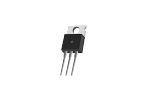
CD4014 IC: 8-Bit Shift Register with Parallel Inputs
This guide explores the CD4014, a highly adaptable CMOS integrated circuit known for its 8-bit shift register functionality, supporting both serial and parallel data inputs. Renowned for its versatility in a wide range of digital logic applications, the CD4014 is effective in scenarios requiring efficient data handling and streamlined transfer, especially in compact systems where reducing pin usage is a priority. From an overview of its pin configurations to applications and alternative options, this article provides an in-depth examination of leveraging the CD4014 for innovative electronic designs and optimized data management.Catalog

Pin Configuration of 4014 IC

|
Pin Name |
Pin No. |
Type |
Description |
|
VDD |
16 |
Power |
Supply Voltage (+3 to +15V) |
|
GND |
8 |
Power |
Ground (0V) |
|
D0-D7 |
1, 4, 5, 6, 7, 13, 14, 15 |
Input |
Parallel data input pins |
|
Q5, Q6, Q7 |
2, 3, 12 |
Output |
Buffered outputs from the last three bits |
|
PE |
9 |
Input |
Parallel Enable |
|
CP |
10 |
Input |
Clock pin to sync the input |
|
Ds |
11 |
Input |
Serial input pin |
Utilization of the 4014 IC
To embark on utilizing the 4014 IC, start by carefully connecting VDD to your power source's positive terminal and GND to the negative terminal. This IC operates within a power range of 3V to 15V, however specific models might extend up to 20V. It's advisable to examine the datasheet for precise electrical details, tailoring compatibility to your unique setup. The chosen voltage range directly influences the device's operational integrity and steady functionality.
Initiate parallel data loading by switching the Parallel Enable (PE) pin into a high state. Connect your chosen data inputs across parallel data pins marked D0 to D7. A rising edge signal applied to the CLK pin captures the intended data into the register. This preparatory phase mirrors setting a team on a well-coordinated practice, where roles and synchronization are of utmost importance.
Commence data shifting by toggling the PE pin to a low state. Each rising CLK pulse shifts data incrementally. In this mode, the DS pin serves for serial data input, facilitating flexible data processing. This function becomes notably beneficial when fluid data transition is needed, ensuring efficient organization and categorization of digital signals.
Application Circuit of the CD4014

The CD4014 shift register is a practical tool for reading the states of up to eight switches using just three microcontroller pins, such as with an Arduino. This makes it ideal for projects where pin availability is limited, as it efficiently expands input capacity without the need for extra hardware. The circuit works by capturing the states of all connected switches and sending this data to the microcontroller one bit at a time. The CD4014 uses parallel-to-serial conversion, allowing you to monitor multiple switches while keeping the wiring simple and compact.
To set it up, connect the Arduino’s D3 pin to the CD4014’s Parallel Enable (PE) pin, D2 to the Clock (CLK) pin, and D4 to the Data Output (Q) pin. D3 activates the latch to capture switch states, D2 sends clock pulses to shift the states into the output, and D4 reads the data sequentially. Each clock pulse shifts the next switch state to the output pin, allowing the Arduino to read all eight switches one at a time. This approach is efficient and saves both space and resources. By using the CD4014, you can manage multiple inputs with minimal I/O usage, simplify your design, and reduce wiring complexity. It’s a compact and reliable solution for projects that require precise monitoring of switch states.
CD4014 Equivalents and Alternatives
Equivalents
• NTE4014
• MC14014
• HCF4014
• HEF4014
• CD4014BE
Alternatives
• 74HC165
• 74HC166
• 74HC198
Datasheet
CD4014BE Datasheets:
Cylindrical Battery Holders.pdf
About us
ALLELCO LIMITED
Read more
Quick inquiry
Please send an inquiry, we will respond immediately.
IRFZ44N MOSFET: Pinout, Arduino Interface, and Features
on December 9th

CD4015 IC: Exploring Its Two 4-Bit Shift Register Design
on December 8th
Popular Posts
-

Complex Instruction Set Computers: How They Changed Computing?
on April 18th 147749
-

USB-C Pinout and Features
on April 18th 111901
-

Using Xilinx Unified Simulation Primitives: A Comprehensive Guide to FPGA Design and Simulation
on April 18th 111349
-

Power Supply Voltages in Electronics: Meaning of VCC, VDD, VEE, VSS, and GND
on April 18th 83714
-

RJ45 Connector Guide: Pinout, Wiring, Cable Types, and Uses
on January 1th 79502
-

The Ultimate Guide to Wire Color Codes in Modern Electrical Systems
The way our electrical systems use colors isn’t just for looks. Each wire color now indicates a specific function, making it easier to identify and handle electrical components correctly during ins...on January 1th 66866
-

Quality (Q) Factor: Equations and Applications
The quality factor, or 'Q', is important when checking how well inductors and resonators work in electronic systems that use radio frequencies (RF). 'Q' measures how well a circuit minimizes energy...on January 1th 63004
-

Purge Valve Guide: Function, Symptoms, Testing, and Replacement for Optimal Engine Performance
The purge valve is a key part of a car’s system that helps keep the air clean by managing fuel vapors before they can escape into the atmosphere. This not only helps the environment by reducing pol...on January 1th 62935
-

Achieving Peak Performance with the Maximum Power Transfer Theorem
The Maximum Power Transfer Theorem explains how energy from a source, such as a battery or generator, flows to a connected load. It shows the exact condition where the load receives the most power....on January 1th 54074
-

A23 Battery Specifications and Compatibility
The A23 battery is a small, cylinder-shaped battery with high voltage. Also called 23A, 23AE, or MN21, it runs at 12 volts and much higher than AA or AAA batteries. Its special design make...on January 1th 52087
HOT Part Number
-

XC3S50A-4VQG100C
AMD
IC FPGA 68 I/O 100VQFP
SI1102-A-GM
Silicon Labs
SENSOR OPT REFLECTIVE 50CM 8WDFN
TCN4-13+
Mini-Circuits
1:4 LTCC TRANSFORMER, 650 - 1250
VF30100S-E3/4W
Vishay General Semiconductor - Diodes Division
DIODE SCHOTTKY 100V 30A ITO220AB
GRM033R70J103KA01D
Murata Electronics
CAP CER 10000PF 6.3V X7R 0201
QMK212B7102MDHT
Taiyo Yuden
CAP CER 1000PF 250V X7R 0805
M82351G-12
MACOM Technology Solutions
ACCESS VOICE PROCESSOR
74LV132D,112
Nexperia USA Inc.
IC GATE NAND SCHMIT 4CH 2IN 14SO
AH1801-FJG-7
Diodes Incorporated
MAG SWITCH OMNIPOLAR DFN2020B-3
DG412DY-T1-E3
Vishay Siliconix
IC SWITCH SPST-NOX4 35OHM 16SOIC
PIC16F876A-I/SO
Microchip Technology
IC MCU 8BIT 14KB FLASH 28SOIC
LXA08FP600
Power Integrations
DIODE GP 600V 8A TO220 FULL PACK
FM25V20A-DG
Infineon Technologies
IC FRAM 2MBIT SPI 40MHZ 8DFN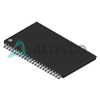
CY7C1011CV33-10ZXC
Cypress Semiconductor Corp
IC SRAM 2MBIT PARALLEL 32TSOP II
04023C221KAT2A
KYOCERA AVX
CAP CER 220PF 25V X7R 0402
RO3101A
Murata Electronics
SAW RES 433.9200MHZ SMD
XRD9818ACGTR
MaxLinear, Inc.
IC AFE 3 CHAN 16BIT 28TSSOP
CL21F104ZBANNNC
Samsung Electro-Mechanics
CAP CER 0.1UF 50V Y5V 0805 -

BZT52-B16_R1_00001
Panjit International Inc.
SOD-123, ZENER
P0300ECL
Littelfuse Inc.
THYRISTOR 25V 400A TO226-2
TPS73615DBVTG4
Texas Instruments
IC REG LINEAR 1.5V 400MA SOT23-5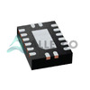
SN74AXC4T774BQBR
Texas Instruments
IC TRANSCEIVER HALF 4/4 16WQFN
170M5954
Eaton - Bussmann Electrical Division
FUSE SQUARE 350A 1KVAC RECT
CC0805KRX7R9BB682
YAGEO
CAP CER 6800PF 50V X7R 0805
SRP7028A-6R8M
Bourns Inc.
FIXED IND 6.8UH 4.5A 60 MOHM SMD
SMAJ150CA
Taiwan Semiconductor Corporation
TVS DIODE 150VWM 243VC DO214AC
PE-68675
Pulse Electronics
IC CHIP
MAX14890EATJ+
Analog Devices Inc./Maxim Integrated
IC RECEIVER 0/4 32TQFN
TFZGTR20B
Rohm Semiconductor
DIODE ZENER 20V 500MW TUMD2
1N5406-E3/73
Vishay General Semiconductor - Diodes Division
DIODE GEN PURP 600V 3A DO201AD
ME501610
Powerex Inc.
BRIDGE RECT 3P 1.6KV 100A MODULE
GRM1555C2A5R8DA01D
Murata Electronics
CAP CER 5.8PF 100V C0G/NP0 0402
MRF8S19140HSR3
NXP USA Inc.
FET RF 65V 1.96GHZ NI780HS
TN2130K1-G
Microchip Technology
MOSFET N-CH 300V 85MA TO236AB
ADL5519ACPZ-R7
Analog Devices Inc.
IC AMP LOG DETECT CTRLR 32LFCSP
SP3222ECT-L
MaxLinear, Inc.
IC TRANSCEIVER FULL 2/2 18SOIC -
502AT-2
Semitec USA Corp
NTC THERMISTORS 5KOHM 1%
NFM18CC101R1C3D
Murata Electronics
CAP FEEDTHRU 100PF 20% 16V 0603
PS2562L-1-F3-A
Renesas Electronics America Inc
OPTOISOLATOR 5KV DARL 4SMD
502494-0370
Affinity Medical Technologies - a Molex company
2.0 W/B SGL R/ARECASSY3CKTEMBSTP
C1206C223K5RACTU
KEMET
CAP CER 0.022UF 50V X7R 1206
NIS5102QP2HT1G
onsemi
IC HOT SWAP CTRLR GP 12PLLP
VI-J62-MY
Vicor Corporation
DC DC CONVERTER 15V 50W
ADR441ARMZ-REEL7
Analog Devices Inc.
IC VREF SERIES 0.12% 8MSOP
MIC5200-5.0BS
Microchip Technology
IC REG LINEAR 5V 100MA SOT223-3
TAS3251DKQR
Texas Instruments
IC AMP D MONO/STER 350W 56HSSOP
GRM1886T1H360JD01D
Murata Electronics
CAP CER 36PF 50V T2H 0603
TZM5249B-GS08
Vishay General Semiconductor - Diodes Division
DIODE ZENER 19V 500MW SOD80
LM2575-5.0YWM
Microchip Technology
IC REG BUCK 5V 1A 24SOIC
RT0402BRE075K6L
YAGEO
RES SMD 5.6K OHM 0.1% 1/16W 0402
C0603JB1A104M030BC
TDK Corporation
CAP CER 0.1UF 10V JB 0201
CSD17571Q2
Texas Instruments
MOSFET N-CH 30V 22A 6SON
P4SMA13CA
Bourns Inc.
TVS DIODE 11.1VWM 18.2VC DO214AC
AR0144ATSM20XUEA0-DPBR
onsemi
1MP 1/4 CIS SO