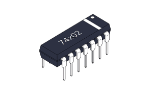
CD4073: A 3-Input AND Gate IC Explained
This guide explores the CD4073, a Triple 3-Input AND Gate integrated circuit, renowned for its versatility and efficiency in modern electronics. It examines the CD4073's role in digital logic circuits by breaking down its pin configurations, gate operations and applications.Catalog

Pin Configuration of 4073 IC

|
Pin Name |
Pin No. |
Type |
Description |
|
VDD |
14 |
Power |
Supply Voltage (+3 to +15V) |
|
GND |
7 |
Power |
Ground (0V) |
|
A1 to A3 |
1, 3, 13 |
Input |
Inputs A of the three AND gates |
|
B1 to B3 |
2, 4, 12 |
Input |
Inputs B of the three AND gates |
|
C1 to C3 |
5, 8, 11 |
Input |
Inputs C of the three AND gates |
|
Q1 to Q3 |
6, 9, 10 |
Output |
Outputs from the three AND gates |
Overview of the 3-Input AND Gate
A 3-input AND gate gives a HIGH output only when all three inputs, referred to as A, B, and C are set to HIGH. Understanding this requires examining the truth table, which offers a detailed display of input combinations illustrating the logical flow to predominantly produce a LOW output. Only with all inputs at HIGH does the circuit generate a HIGH output, embodying the intricate check needed in scenarios demanding stringent condition fulfillment for a desired outcome to occur.

|
Input A |
Input B |
Input C |
Output Q |
|
0 |
0 |
0 |
0 |
|
0 |
0 |
1 |
0 |
|
0 |
1 |
0 |
0 |
|
0 |
1 |
1 |
0 |
|
1 |
0 |
0 |
0 |
|
1 |
0 |
1 |
0 |
|
1 |
1 |
0 |
0 |
|
1 |
1 |
1 |
1 |
Function and Usage of the CD4073
Initial Setup and Connections
To initiate the deployment of the CD4073, begin by connecting VDD to a stable and positive voltage supply, while ensuring that GND is securely linked to the ground. This step serves as the backbone for the integrated circuit's proper functioning. It's advisable to double-check these connections to circumvent any potential discrepancies that could arise from power issues.
Input and Signal Management
The inputs, labeled A, B, and C, are to be connected to digital signals that accurately reflect the conditions under examination. The choice of digital signals holds an impact because it predicates the logic and behavior processed by the CD4073. Neglect or oversight, such as stray connections or noise, may introduce errors, complicating the logical operations.
Output Utilization and Circuit Integration
The gate outputs, usually represented as Q, act as the logical intersection indicators of inputs A, B, and C. Integrating these outputs into subsequent circuit operations can provide immense value. Strategic integration is often guided by past scenarios where optimizing circuit efficiency led to notable performance enhancements.
CD4073 Application Circuit
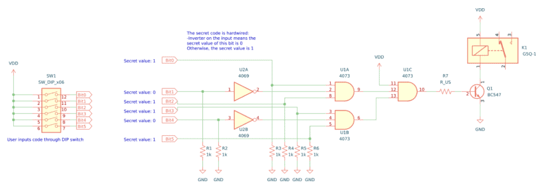
The CD4073 integrated circuit is an important component for building a secure code lock system that verifies a 6-bit binary code, such as 101101. This system utilizes the AND gates within the CD4073 to confirm the accuracy of the input code. NOT gates from an IC like the CD4069BE are used to adjust logic levels, ensuring the input is correctly interpreted by the circuit. Proper sequencing and adjustment of the input logic are needed for the system to function reliably.
Several components are key to assembling the circuit. A relay is used to control external devices, while the CD4073BE handles the AND gate operations, and the CD4069BE provides NOT gate operations. A 6-position DIP switch is used for inputting the binary code, and resistors are included to regulate current flow. An NPN transistor, such as the BC547, is employed to power the relay and ensure proper operation.
The relay is activated by the transistor, which amplifies the small current from the DIP switch to drive the relay. This allows the circuit to regulate external devices like security alarms or door locks, enhancing overall security. The proper selection and biasing of the transistor are required to avoid circuit errors. This demonstrates the importance of balancing digital logic with analog control, as their careful interaction determines the success or failure of hardware applications.
CD4073 Alternatives and Equivalents
• Also labeled as NTE4073, MC14073, HCF4073, TC4073, HEF4073.
• Variations like "CD4073BE" indicate manufacturer or technology differences.
• 74HC11: Another triple 3-input AND gate IC.
Datasheets
CD4073BE Datasheets:
About us
ALLELCO LIMITED
Read more
Quick inquiry
Please send an inquiry, we will respond immediately.
Exploring the CD4510 Up/Down Counter with Preset Capability
on December 7th
7400 Series NOR Gates: Exploring 74LS02/74HC02 Features and Applications
on December 7th
Popular Posts
-

Complex Instruction Set Computers: How They Changed Computing?
on April 18th 147749
-

USB-C Pinout and Features
on April 18th 111916
-

Using Xilinx Unified Simulation Primitives: A Comprehensive Guide to FPGA Design and Simulation
on April 18th 111349
-

Power Supply Voltages in Electronics: Meaning of VCC, VDD, VEE, VSS, and GND
on April 18th 83714
-

RJ45 Connector Guide: Pinout, Wiring, Cable Types, and Uses
on January 1th 79502
-

The Ultimate Guide to Wire Color Codes in Modern Electrical Systems
The way our electrical systems use colors isn’t just for looks. Each wire color now indicates a specific function, making it easier to identify and handle electrical components correctly during ins...on January 1th 66872
-

Quality (Q) Factor: Equations and Applications
The quality factor, or 'Q', is important when checking how well inductors and resonators work in electronic systems that use radio frequencies (RF). 'Q' measures how well a circuit minimizes energy...on January 1th 63005
-

Purge Valve Guide: Function, Symptoms, Testing, and Replacement for Optimal Engine Performance
The purge valve is a key part of a car’s system that helps keep the air clean by managing fuel vapors before they can escape into the atmosphere. This not only helps the environment by reducing pol...on January 1th 62949
-

Achieving Peak Performance with the Maximum Power Transfer Theorem
The Maximum Power Transfer Theorem explains how energy from a source, such as a battery or generator, flows to a connected load. It shows the exact condition where the load receives the most power....on January 1th 54077
-

A23 Battery Specifications and Compatibility
The A23 battery is a small, cylinder-shaped battery with high voltage. Also called 23A, 23AE, or MN21, it runs at 12 volts and much higher than AA or AAA batteries. Its special design make...on January 1th 52091
HOT Part Number
-

BD9B100MUV-E2
Rohm Semiconductor
IC REG BUCK ADJ 1A 16VQFN
UPD70F3539AF5A9-PN7-Q-A
Renesas Electronics America Inc
IC MICROCONTROLLER
18081A621JAT2A
KYOCERA AVX
CAP CER 620PF 100V NP0 1808
FDN340P
onsemi
MOSFET P-CH 20V 2A SUPERSOT3
70231-101
Amphenol ICC (FCI)
CONN RCPT BLADE PWR 8POS EDGE MT
MPSW42RLRAG
onsemi
TRANS NPN 300V 0.5A TO92
MC7824BT
onsemi
IC REG LINEAR 24V 1A TO220AB
AD8009ARZ-REEL
Analog Devices Inc.
IC OPAMP CFA 1 CIRCUIT 8SOIC
LT1815CS5#TRPBF
Analog Devices Inc.
IC OPAMP VFB 1 CIRCUIT TSOT23-5
DG411DYZ
Renesas Electronics America Inc
IC SWITCH SPST-NCX4 35OHM 16SOIC
VFT2060C-M3/4W
Vishay General Semiconductor - Diodes Division
DIODE SCHOTTKY 20A 60V ITO-220AB
TSX562AIYST
STMicroelectronics
IC CMOS 2 CIRCUIT 8MINISO
MR256D08BMA45
Everspin Technologies Inc.
IC RAM 256KBIT PARALLEL 48FBGA
VSC3312YYP-01
Microchip Technology
IC SWITCH 16X16 6.5GBPS 196FCBGA
XC68HC908GP20CFB
Motorola
TSG 8BIT20K FLASH
CSR8811A08-ICXR-R
Qualcomm
IC RF TXRX+MCU BLUETOOTH
MPSW05
onsemi
TRANS NPN 60V 0.5A TO92
1N4055R
Solid State Inc.
DIODE GEN PURP REV 900V 275A DO9 -

ASX342ATSC00XPED0-DP
onsemi
IMAGE SENSOR VGA 1/4 CIS SOC
0433.125NR
Littelfuse Inc.
FUSE BOARD MNT 125MA 125VAC/VDC
1SMA5941BT3G
onsemi
DIODE ZENER 47V 1.5W SMA
DCP010512BP-U/700
Texas Instruments
DC DC CONVERTER 12V 1W
1-1734344-1
TE Connectivity AMP Connectors
CONN D-SUB HD RCPT 15P R/A SLDR
KSD1621STF
onsemi
TRANS NPN 25V 2A SOT89-3
BQ24161RGET
Texas Instruments
IC BATT CHG LI-ION 1CELL 24VQFN
BTA26-600BW
STMicroelectronics
TRIAC ALTERNISTOR 600V 25A TOP3
NCP1239DD65R2G
onsemi
IC OFFLINE SWITCH FLYBACK 7SOIC
TMS320TCI6482BZTZA
Texas Instruments
TMS320 - DIGITAL SIGNAL PROCESSO
BQ20Z90DBTR-V150
Texas Instruments
IC GAS GAUGE LI-ION 30TSSOP
PCMB104T-1R0MT
Susumu
FIXED IND 1UH 18A 3.3 MOHM SMD
CY29942AXCT
Infineon Technologies
IC CLK BUFFER 1:18 200MHZ 32TQFP
CC0402KRX7R9BB561
YAGEO
CAP CER 560PF 50V X7R 0402
STPS20M60SG-TR
STMicroelectronics
DIODE SCHOTTKY 60V 20A D2PAK
AT25010N-10SC-2.7
Microchip Technology
IC EEPROM 1KBIT SPI 3MHZ 8SOIC
04023A1R0CAT4A
KYOCERA AVX
CAP CER 1PF 25V C0G/NP0 0402
ISL6327IRZ
Intersil
SWITCHING CONTROLLER, VOLTAGE-MO -

LQW18AN75NG0ZD
Murata Electronics
FIXED IND
DFA100BA160
SanRex Corporation
DIODE MODULE 1600V 100A
BAR46AFILM
STMicroelectronics
DIODE ARRAY SCHOTTKY 100V SOT23
MAX825SEUK
Analog Devices Inc./Maxim Integrated
IC SUPERVISOR MPU
MMST2222A-7-F
Diodes Incorporated
TRANS NPN 40V 0.6A SOT323
FODM8801AR2
onsemi
OPTOISO 3.75KV TRANS 4-MINI-FLAT
FJV1845FMTF
Fairchild Semiconductor
SMALL SIGNAL BIPOLAR TRANSISTOR,
EVK105RH5R1JW-F
Taiyo Yuden
CAP CER 5.1PF 16V R2H 0402
6651170-3
TE Connectivity AMP Connectors
CONN EDGE DUAL FMALE 4POS 0.508
KSZ8893FQLI-FX
Microchip Technology
IC SWITCH ETH 3PORT 128QFP
170M6340
Eaton - Bussmann Electrical Division
FUSE SQUARE 400A 1.3KVAC RECT
BCM20741A2KFB1G
Broadcom Limited
SINGLE-CHIP BLUETOOTH
MAX3443EASA+
Analog Devices Inc./Maxim Integrated
IC TRANSCEIVER HALF 1/1 8SOIC
GRM0335C1H9R3DA01D
Murata Electronics
CAP CER 9.3PF 50V C0G/NP0 0201
TNY175PN
Power Integrations
11.5 W (85-265 VAC) 15 W (230 VA
742700726
Würth Elektronik
FERRITE CORE 278 OHM SOLID 4MM
DM74S20N
onsemi
IC GATE NAND 2CH 4-INP 14DIP
P4SMA56CA-E3/61
Vishay General Semiconductor - Diodes Division
TVS DIODE 47.8VWM 77VC DO214AC