Complete Guide to P-Channel Enhancement MOSFET
You often see MOSFETs used in circuits, but understanding how they actually work can feel confusing at first. A P-channel MOSFET is one of the simplest ways to control current using voltage, especially when working with power lines. As you go through this guide, you will see how its structure, operation, and behavior come together in a clear way. Each section breaks things down into manageable ideas, so you can follow how voltage affects current and how this device is used in real electronic setups.Catalog
Figure 1. P-Channel MOSFET Power Switching Circuit
What Is a P-Channel Enhancement MOSFET
A P-channel enhancement MOSFET is a field-effect transistor that controls current using an electric field. It belongs to the MOSFET family, which is widely used in electronic circuits for switching and control. The term enhancement means the device remains in an off state by default and requires an external voltage to operate.
The device turns on when a negative voltage is applied between the gate and source, expressed as VGS < 0. Once this voltage exceeds a certain level, conduction begins between the source and drain terminals. Because control is achieved through voltage rather than current, the gate draws very little input current, which supports efficient operation.
P-channel enhancement MOSFETs are commonly used in circuits that require controlled switching, especially when the switching element is placed on the positive side of a power source, allowing simple and effective control of power flow.
P-Channel MOSFET Structure and Terminals
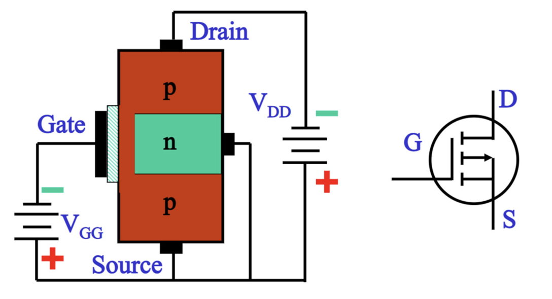
Figure 2. P-Channel MOSFET Structure and Symbol
A P-channel MOSFET is built on an N-type substrate with two P-type regions formed within it, which act as the source and drain. These regions are placed on opposite sides, defining the area where current flows through the device.
A thin layer of silicon dioxide (SiO₂) is positioned above this region and serves as an electrical insulator, separating the semiconductor material from the gate. This allows the gate to influence the device without direct electrical contact.
The gate terminal sits above this insulating layer, aligned between the source and drain, and acts as the control point where voltage is applied. The source provides the charge carriers, while the drain serves as the terminal where current exits.
In most practical designs, the body or substrate is internally connected to the source, which simplifies the structure into a three-terminal device and makes it easier to use in standard circuits.
How a P-Channel MOSFET Works
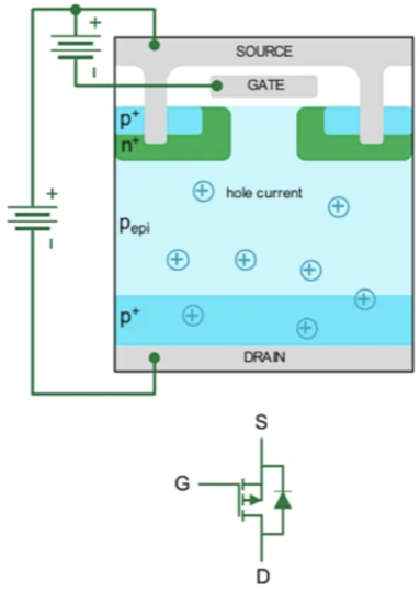
Figure 3. P-Channel MOSFET Working Principle
The operation of a P-channel MOSFET begins when a negative voltage is applied between the gate and source, creating an electric field across the insulating layer that influences the region beneath the gate. As this voltage increases, holes are drawn toward the area under the gate, where they accumulate near the surface of the substrate and gradually form a conductive path between the source and drain.
Once this path is established, applying a drain-to-source voltage allows current to flow through the channel, driven by the movement of holes from the source toward the drain. In this way, the gate voltage controls the formation of the path, while the drain voltage drives the current through it, showing a clear relationship between applied voltage and device behavior.
Operating Regions of a P-Channel MOSFET
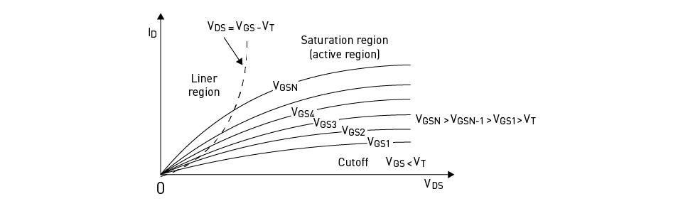
Figure 4. P-Channel MOSFET Operating Regions
Cutoff Region
In the cutoff region, the gate-to-source voltage is not sufficiently negative to allow conduction, so the device remains in an off state. Under this condition, there is no effective path for current flow between the source and drain, and the drain current is essentially zero. On the graph, this region appears along the horizontal axis where current remains negligible.
Linear Region
In the linear region, the MOSFET begins to conduct, and the drain current increases as the drain-to-source voltage increases. The curves rise steadily in this region, showing that current responds directly to changes in voltage. The device behaves like a variable resistor, where the level of current depends on both the gate voltage and the applied drain voltage. This region is useful when controlled variation of current is required.
Saturation Region
In the saturation region, the curves begin to flatten, indicating that the drain current no longer increases significantly with further changes in drain voltage. The device operates in a more stable condition, providing a nearly constant current for a given gate voltage. Each curve represents a different gate voltage level, and higher negative gate voltages result in higher current levels in this region.
Pinch-Off Condition and Current Control in MOSFET
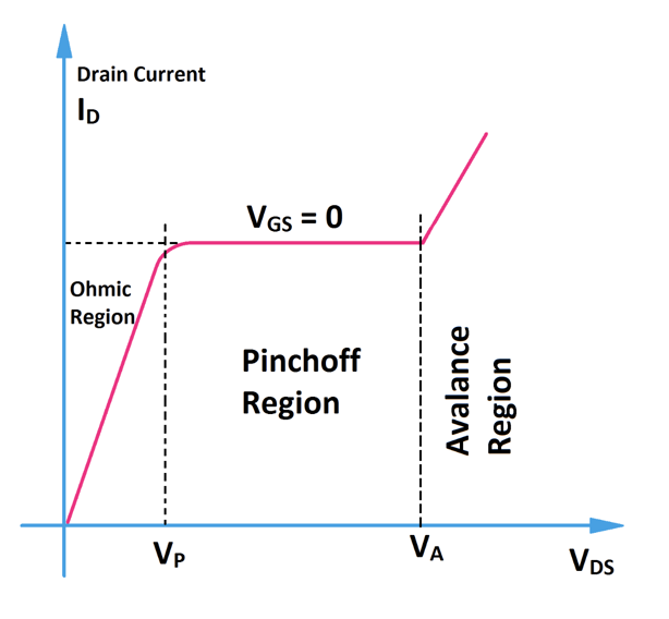
Figure 5. MOSFET Pinch-Off and Current Behavior
The pinch-off condition occurs when the conductive channel inside the MOSFET becomes narrow near the drain terminal as the drain-to-source voltage increases, caused by the expansion of the depletion region that reduces the effective channel width at that end.
As this narrowing develops, further increases in drain voltage no longer produce a significant increase in current, since the restricted channel limits additional flow even though conduction continues through the device. This behavior appears in the characteristic curve where the current levels begin to flatten after a certain voltage, indicating that the current is no longer dependent on the drain voltage.
In this condition, the drain current is primarily controlled by the gate-to-source voltage (VGS), where adjusting this voltage changes the channel width and directly sets the current level.
V-I Characteristics of a P-Channel MOSFET
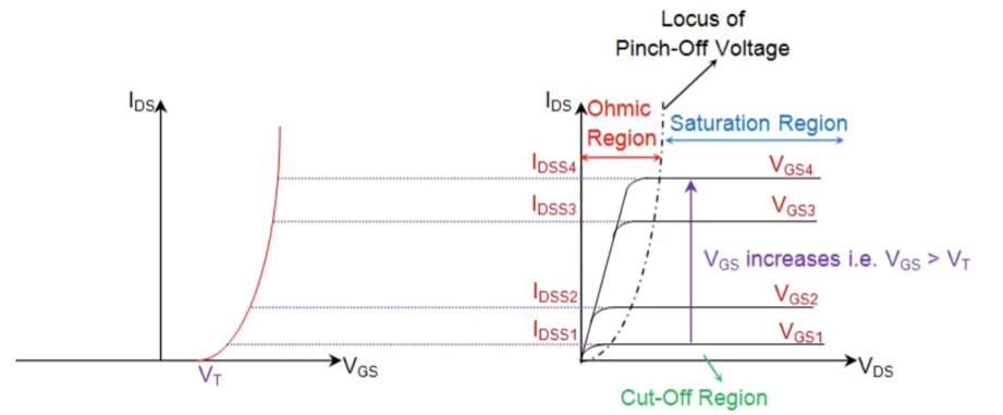
Figure 6. P-Channel MOSFET V-I Characteristics
The V-I characteristics of a P-channel MOSFET show how the drain current (ID) varies with drain-to-source voltage (VDS) under different gate-to-source voltages (VGS). These relationships are presented as a set of curves, with each curve representing a specific gate voltage level.
Each curve corresponds to a different VGS, and as the magnitude of this voltage increases, the curves shift upward, indicating higher current levels. This makes it clear that the current through the device is strongly influenced by the applied gate voltage.
At lower values of VDS, the curves rise with a noticeable slope, showing that current increases as the drain voltage increases. As VDS continues to increase, the curves gradually flatten, indicating that the current becomes less dependent on further changes in drain voltage.
Difference Between P-Channel and N-Channel MOSFET
Figure 7. P-Channel vs N-Channel MOSFET Circuits
The difference between P-channel and N-channel MOSFETs is mainly defined by their voltage requirements, charge carriers, and performance characteristics, all of which influence how they are used in circuits.
A P-channel MOSFET turns on when a negative gate-to-source voltage (VGS) is applied, while an N-channel MOSFET requires a positive VGS, and this difference in polarity affects how each device is driven and positioned within a circuit, especially when controlling different sides of a power supply.
The two devices also differ in the type of charge carriers involved. P-channel MOSFETs use holes, whereas N-channel MOSFETs use electrons, and because electrons move more easily through semiconductor material, N-channel devices generally provide better conductivity and faster response.
This leads to differences in performance, where N-channel MOSFETs typically offer lower resistance and higher efficiency, making them suitable for high-speed and high-current applications, while P-channel MOSFETs are often preferred for high-side switching, where control of the positive supply line is required, even though their performance is generally lower.
Applications of P-Channel MOSFET
A P-channel MOSFET is commonly used in circuits where simple and reliable control of current is required, especially on the positive side of a power supply. Its ability to turn on with a negative gate voltage makes it suitable for configurations where direct control of the supply line is needed.
One common application is high-side switching, where the MOSFET is placed between the power source and the load. In this setup, it allows the circuit to connect or disconnect power without interrupting the ground path, which helps maintain stable operation in many systems.
It is also used in power control circuits, where it regulates the flow of current to components such as sensors, microcontrollers, or small electronic modules. This makes it useful in battery-powered devices, where controlled power delivery helps manage energy use.
In addition, P-channel MOSFETs are often found in load switching and protection circuits, where they help prevent unwanted current flow or allow selective control of different parts of a system. These applications rely on the device’s ability to provide simple and effective switching with minimal control complexity.
Advantages and Limitations of P-Channel MOSFET
| Advantages | Limitations |
| Simple high-side switching | Higher on-resistance compared to N-channel |
| Easier gate drive in some circuits | Lower current capability |
| Works well with positive supply control | Slower switching speed |
| Minimal gate current required | Lower efficiency in high-power applications |
| Suitable for low-voltage systems | Higher power loss due to resistance |
| Simple circuit design implementation | Larger device size for same performance |
| No need for complex driver in basic setups | More heat generation under load |
| Good for load switching and protection | Less suitable for high-frequency operation |
| Compatible with battery-powered devices | Limited performance in high-current designs |
| Stable operation in basic control circuits | Generally higher cost for equivalent performance |
Conclusion
A P-channel MOSFET gives you a simple way to control current using voltage, which makes it useful in many basic circuits. You can see how its structure supports its operation, and how voltage directly affects current flow. As you move through its operating regions and characteristics, the behavior becomes easier to understand. The comparison with N-channel devices also helps clarify when to use each type. In real circuits, it is often chosen for high-side switching and simple control tasks. While it has some limitations, it still works well in many practical setups. Understanding these basics helps you use it more confidently in your designs.
About us
ALLELCO LIMITED
Read more
Quick inquiry
Please send an inquiry, we will respond immediately.
Frequently Asked Questions [FAQ]
1. What is a P-channel MOSFET used for?
It is mainly used for switching and controlling current, especially on the positive side of a power supply.
2. Why does a P-channel MOSFET need a negative gate voltage?
A negative gate-to-source voltage allows the device to turn on and conduct current.
3. What is pinch-off in a MOSFET?
Pinch-off is the point where the channel narrows and the current stops increasing with higher drain voltage.
4. Which is better, P-channel or N-channel MOSFET?
N-channel MOSFETs usually perform better, but P-channel MOSFETs are easier to use in high-side switching.
5. Does a MOSFET require current at the gate?
No, it is controlled by voltage, so the gate draws very little current.

IPC-A-610 Standard: Everything You Need to Know About PCBA Quality
on March 21th
What Makes HDI PCB Different From Standard PCB
on March 20th
Popular Posts
-

Complex Instruction Set Computers: How They Changed Computing?
on April 18th 147749
-

USB-C Pinout and Features
on April 18th 111904
-

Using Xilinx Unified Simulation Primitives: A Comprehensive Guide to FPGA Design and Simulation
on April 18th 111349
-

Power Supply Voltages in Electronics: Meaning of VCC, VDD, VEE, VSS, and GND
on April 18th 83714
-

RJ45 Connector Guide: Pinout, Wiring, Cable Types, and Uses
on January 1th 79502
-

The Ultimate Guide to Wire Color Codes in Modern Electrical Systems
The way our electrical systems use colors isn’t just for looks. Each wire color now indicates a specific function, making it easier to identify and handle electrical components correctly during ins...on January 1th 66869
-

Quality (Q) Factor: Equations and Applications
The quality factor, or 'Q', is important when checking how well inductors and resonators work in electronic systems that use radio frequencies (RF). 'Q' measures how well a circuit minimizes energy...on January 1th 63004
-

Purge Valve Guide: Function, Symptoms, Testing, and Replacement for Optimal Engine Performance
The purge valve is a key part of a car’s system that helps keep the air clean by managing fuel vapors before they can escape into the atmosphere. This not only helps the environment by reducing pol...on January 1th 62943
-

Achieving Peak Performance with the Maximum Power Transfer Theorem
The Maximum Power Transfer Theorem explains how energy from a source, such as a battery or generator, flows to a connected load. It shows the exact condition where the load receives the most power....on January 1th 54076
-

A23 Battery Specifications and Compatibility
The A23 battery is a small, cylinder-shaped battery with high voltage. Also called 23A, 23AE, or MN21, it runs at 12 volts and much higher than AA or AAA batteries. Its special design make...on January 1th 52088
HOT Part Number
-

BD9B100MUV-E2
Rohm Semiconductor
IC REG BUCK ADJ 1A 16VQFN
UPD70F3539AF5A9-PN7-Q-A
Renesas Electronics America Inc
IC MICROCONTROLLER
18081A621JAT2A
KYOCERA AVX
CAP CER 620PF 100V NP0 1808
FDN340P
onsemi
MOSFET P-CH 20V 2A SUPERSOT3
70231-101
Amphenol ICC (FCI)
CONN RCPT BLADE PWR 8POS EDGE MT
MPSW42RLRAG
onsemi
TRANS NPN 300V 0.5A TO92
MC7824BT
onsemi
IC REG LINEAR 24V 1A TO220AB
AD8009ARZ-REEL
Analog Devices Inc.
IC OPAMP CFA 1 CIRCUIT 8SOIC
LT1815CS5#TRPBF
Analog Devices Inc.
IC OPAMP VFB 1 CIRCUIT TSOT23-5
DG411DYZ
Renesas Electronics America Inc
IC SWITCH SPST-NCX4 35OHM 16SOIC
VFT2060C-M3/4W
Vishay General Semiconductor - Diodes Division
DIODE SCHOTTKY 20A 60V ITO-220AB
TSX562AIYST
STMicroelectronics
IC CMOS 2 CIRCUIT 8MINISO
MR256D08BMA45
Everspin Technologies Inc.
IC RAM 256KBIT PARALLEL 48FBGA
VSC3312YYP-01
Microchip Technology
IC SWITCH 16X16 6.5GBPS 196FCBGA
XC68HC908GP20CFB
Motorola
TSG 8BIT20K FLASH
CSR8811A08-ICXR-R
Qualcomm
IC RF TXRX+MCU BLUETOOTH
MPSW05
onsemi
TRANS NPN 60V 0.5A TO92
1N4055R
Solid State Inc.
DIODE GEN PURP REV 900V 275A DO9 -

ASX342ATSC00XPED0-DP
onsemi
IMAGE SENSOR VGA 1/4 CIS SOC
0433.125NR
Littelfuse Inc.
FUSE BOARD MNT 125MA 125VAC/VDC
1SMA5941BT3G
onsemi
DIODE ZENER 47V 1.5W SMA
DCP010512BP-U/700
Texas Instruments
DC DC CONVERTER 12V 1W
1-1734344-1
TE Connectivity AMP Connectors
CONN D-SUB HD RCPT 15P R/A SLDR
KSD1621STF
onsemi
TRANS NPN 25V 2A SOT89-3
BQ24161RGET
Texas Instruments
IC BATT CHG LI-ION 1CELL 24VQFN
BTA26-600BW
STMicroelectronics
TRIAC ALTERNISTOR 600V 25A TOP3
NCP1239DD65R2G
onsemi
IC OFFLINE SWITCH FLYBACK 7SOIC
TMS320TCI6482BZTZA
Texas Instruments
TMS320 - DIGITAL SIGNAL PROCESSO
BQ20Z90DBTR-V150
Texas Instruments
IC GAS GAUGE LI-ION 30TSSOP
PCMB104T-1R0MT
Susumu
FIXED IND 1UH 18A 3.3 MOHM SMD
CY29942AXCT
Infineon Technologies
IC CLK BUFFER 1:18 200MHZ 32TQFP
CC0402KRX7R9BB561
YAGEO
CAP CER 560PF 50V X7R 0402
STPS20M60SG-TR
STMicroelectronics
DIODE SCHOTTKY 60V 20A D2PAK
AT25010N-10SC-2.7
Microchip Technology
IC EEPROM 1KBIT SPI 3MHZ 8SOIC
04023A1R0CAT4A
KYOCERA AVX
CAP CER 1PF 25V C0G/NP0 0402
ISL6327IRZ
Intersil
SWITCHING CONTROLLER, VOLTAGE-MO -

LQW18AN75NG0ZD
Murata Electronics
FIXED IND
DFA100BA160
SanRex Corporation
DIODE MODULE 1600V 100A
BAR46AFILM
STMicroelectronics
DIODE ARRAY SCHOTTKY 100V SOT23
MAX825SEUK
Analog Devices Inc./Maxim Integrated
IC SUPERVISOR MPU
MMST2222A-7-F
Diodes Incorporated
TRANS NPN 40V 0.6A SOT323
FODM8801AR2
onsemi
OPTOISO 3.75KV TRANS 4-MINI-FLAT
FJV1845FMTF
Fairchild Semiconductor
SMALL SIGNAL BIPOLAR TRANSISTOR,
EVK105RH5R1JW-F
Taiyo Yuden
CAP CER 5.1PF 16V R2H 0402
6651170-3
TE Connectivity AMP Connectors
CONN EDGE DUAL FMALE 4POS 0.508
KSZ8893FQLI-FX
Microchip Technology
IC SWITCH ETH 3PORT 128QFP
170M6340
Eaton - Bussmann Electrical Division
FUSE SQUARE 400A 1.3KVAC RECT
BCM20741A2KFB1G
Broadcom Limited
SINGLE-CHIP BLUETOOTH
MAX3443EASA+
Analog Devices Inc./Maxim Integrated
IC TRANSCEIVER HALF 1/1 8SOIC
GRM0335C1H9R3DA01D
Murata Electronics
CAP CER 9.3PF 50V C0G/NP0 0201
TNY175PN
Power Integrations
11.5 W (85-265 VAC) 15 W (230 VA
742700726
Würth Elektronik
FERRITE CORE 278 OHM SOLID 4MM
DM74S20N
onsemi
IC GATE NAND 2CH 4-INP 14DIP
P4SMA56CA-E3/61
Vishay General Semiconductor - Diodes Division
TVS DIODE 47.8VWM 77VC DO214AC