Complete Guide to the ATmega328P Microcontroller: Features, Architecture, Pinout, and Applications
This guide explains everything you need to know about the ATmega328P microcontroller, a small but powerful chip used in many electronics. You'll learn what it does, how it works, how to connect it, and where it’s used. Whether you're making a school project, building a robot, or using an Arduino board, this guide will help you understand why the ATmega328P is such a popular choice in electronics.Catalog

Overview of the ATmega328P Microcontroller
The ATmega328P, made by Microchip Technology, is an 8-bit microcontroller from the AVR family. It's well-known for balancing speed and power efficiency, especially in battery-powered devices. It runs on a RISC (Reduced Instruction Set Computing) architecture and is built using CMOS technology, which helps reduce power usage while still supporting fast processing. Most instructions complete in just one clock cycle, allowing the chip to deliver up to 1 MIPS per MHz. This efficiency is a key reason the ATmega328P is often used in low-power systems that still require reliable performance.
With features like analog-to-digital conversion, serial communication (USART, SPI, I²C), and interrupt support, the chip fits well in everything from simple gadgets to more complex industrial controllers. It runs at up to 20 MHz and works within a voltage range of 1.8V to 5.5V, making it flexible across many hardware setups. Memory includes 32 KB of flash, 1 KB of EEPROM, and 2 KB of SRAM, enough to handle complex algorithms and data. It also includes built-in peripherals like timers, a watchdog timer, and counters, which improve system reliability. One of its most recognizable uses is on the Arduino UNO board. Its ability to scale from prototypes to final products makes it a solid foundation for a wide range of embedded applications.
ATmega328P Features and Performance
The ATmega328P is built on a compact yet powerful Reduced Instruction Set Computing (RISC) architecture, supporting 131 distinct instructions. The majority of these instructions execute in a single clock cycle, enabling the microcontroller to achieve performance levels of up to 16 Million Instructions Per Second (MIPS) when operating at a 16 MHz clock speed. This high efficiency makes the ATmega328P well-suited for applications required processing speed and low power consumption. At the core of its processing capabilities are 32 general-purpose 8-bit registers, which are directly connected to the Arithmetic Logic Unit (ALU), allowing for faster and more flexible data manipulation. The ATmega328P includes a two-cycle hardware multiplier, improving performance for arithmetic operations for applications involving signal processing, control systems, and sensor data handling. The microcontroller operates in static mode, allowing it to maintain stable performance across a wide range of operating conditions, including varying system activity levels. This stability is valuable in embedded systems, where power states and task loads can fluctuate dynamically.
The memory architecture of the ATmega328P is designed to efficiently support both code storage and runtime data handling. It includes 32 KB of In-System Programmable Flash memory, which enables self-programming via the onboard bootloader and supports up to 10,000 write cycles. This feature allows firmware updates to be performed directly on the device without the need for physical removal or external programming tools. The microcontroller provides 1 KB of EEPROM, offering up to 100,000 write/erase cycles, making it ideal for storing non-volatile configuration data or user-defined settings that need to persist between power cycles. Complementing this is 2 KB of SRAM, which handles temporary data such as variables, stacks, and buffers during processing.
To ensure secure and flexible development, the ATmega328P incorporates several useful security features. These include locked boot sections to prevent unauthorized code modification, read-while-write capabilities in flash memory for efficient firmware updates, and an on-chip bootloader that enables firmware installation or upgrades through standard serial interfaces, eliminating the need for specialized external programmers. For precise timing and scheduling tasks, the microcontroller features a robust system of hardware timers: two 8-bit timers and one 16-bit timer, each equipped with compare and capture features. These timers are important for generating accurate pulse-width modulation (PWM) signals, performing event timing, and managing scheduled tasks. Such capabilities are valuable in applications like motor control, signal generation, and communication protocols.
ATmega328P Microcontroller Pin Configurations
The ATmega328P microcontroller is available in two primary pin configurations, which vary based on the package type. These configurations include the TQFP (Thin Quad Flat Package) and the MLF (Micro Lead Frame), also known as QFN (Quad Flat No-lead), both of which feature 32 pins. Both versions use a 32-pin layout but are physically different in form factor. The internal functionality of the pins remains consistent across these packages, with identical signal assignments and numbering.

Figure 2. ATmega328P TQFP Pinout

Figure 3. ATmega328P MLF Pinout
Pin Descriptions
VCC
Supplies digital power to the chip.
GND
Connects to ground.
Port B (PB7:0) – XTAL1, XTAL2, TOSC1, TOSC2
Port B is an 8-bit input/output port with internal pull-up resistors (enabled individually per pin). It can both source and sink current with balanced drive strength. When used as input and pulled low externally, the port sources current if pull-ups are enabled. During a reset, Port B pins go into a high-impedance (tri-state) mode, regardless of the clock status. PB6 and PB7 may be used for oscillator functions based on clock fuse settings. When using the internal RC oscillator and enabling asynchronous Timer/Counter2 (via the AS2 bit), PB6 and PB7 act as TOSC1 and TOSC2.
Port C (PC5:0)
Port C is a 7-bit bi-directional I/O port with internal pull-ups (selectable per pin). The pins have strong, balanced drive characteristics. If a pin is pulled low externally and the pull-up is enabled, it sources current. During reset, the pins enter tri-state mode.
PC6 / RESET
PC6 functions either as a general input pin or a reset pin. If the RSTDISBL fuse is not programmed, PC6 acts as a reset input. A low signal lasting longer than a defined minimum duration triggers a reset (even without a running clock). If the fuse is programmed, the pin is used as a regular input.
Port D (PD7:0)
Port D is an 8-bit bidirectional port, also with selectable pull-up resistors and balanced output strength. Like the other ports, it sources current when externally pulled low (if pull-ups are enabled), and enters tri-state mode during reset.
AVCC
AVCC powers the analog-to-digital converter (ADC), PC3:0, and ADC channels 6 and 7. It should be connected to VCC, even if the ADC isn't used. When using the ADC, connect AVCC to VCC through a low-pass filter. Note that pins PC6–PC4 still use digital VCC.
AREF
This is the analog reference voltage input for the ADC.
ADC7:6 (TQFP and QFN/MLF Packages Only)
In the TQFP and QFN/MLF package versions, these pins serve as analog inputs for the ADC. They are powered via the analog voltage supply and function as 10-bit resolution ADC channels.
ATmega328p Microcontroller Electrical Characteristics
|
Parameters |
Min. |
Typ. |
Max. |
Unit |
|
Operating temperature |
–55 |
125 |
°C |
|
|
Storage temperature |
–65 |
150 |
°C |
|
|
Voltage on any pin except RESET with respect to ground |
–0.5 |
VCC + 0.5 |
V |
|
|
Voltage on RESET with respect to ground |
–0.5 |
+13.0 |
V |
|
|
Maximum operating voltage |
6.0 |
V |
||
|
DC current per I/O pin |
40.0 |
mA |
||
|
DC current VCC and GND pins |
200.0 |
mA |
||
|
Injection current at VCC = 0V |
±5.0 |
mA |
||
|
Injection current at VCC = 5V |
±1.0 |
mA |
ATmega328p Architecture and Internal Blocks

Figure 4. ATmega328p Architecture and Internal Blocks
At the heart of the ATmega328P is an AVR CPU core, which connects 32 general-purpose registers directly to the Arithmetic Logic Unit (ALU). This architecture allows two registers to be accessed within a single clock cycle, improving the execution speed and overall efficiency of the microcontroller. The CPU sits centrally in the system and connects to various memory blocks and peripheral modules through an internal data bus, as shown in the diagram. The memory system includes three primary types. Flash memory, with 32 KB capacity, stores the firmware and supports self-programming for in-field updates. EEPROM, sized at 1 KB, retains data even when power is lost, making it ideal for storing persistent configurations. SRAM, with 2 KB of space, serves as the MCU’s temporary working memory, enabling data processing during active operations. All three memory types are mapped into the system's internal data bus, ensuring fast access and communication with the CPU.
The ATmega328P integrates several peripherals that expand its functionality. It includes two 8-bit timers (T/C0 and T/C2) and one 16-bit timer (T/C1), which are used for precise timekeeping, pulse-width modulation (PWM), and event counting. The Analog-to-Digital Converter (ADC) provides eight input channels and a 10-bit resolution, offering accurate sampling of analog signals from sensors or external inputs. An internal bandgap reference and an analog comparator support stable voltage references and analog signal comparisons. Communication capabilities are robust, with three key interfaces: USART for serial communication, SPI for high-speed synchronous data exchange, and TWI (also known as I²C) for connecting to external peripherals over two wires. These modules are closely connected to the I/O ports (PORT B and PORT C), giving flexibility in system design. The block diagram clearly illustrates these interconnections, showing how data flows between the peripherals and the AVR core.
To ensure system stability, a watchdog timer is included, operating with its own oscillator to reset the microcontroller if the software becomes unresponsive. This is important in embedded systems that must run unattended for long periods. The interrupt system enhances responsiveness by allowing immediate reactions to both internal events (like timer overflows or ADC conversions) and external inputs (such as pin changes). Power management is another key strength of the ATmega328P. The microcontroller supports multiple sleep modes that reduce power consumption by disabling unused modules while maintaining the necessary system states. Features like Power-On Reset (POR) and Brown-Out Detection (BOD) help maintain reliable operation during startup and under fluctuating voltage conditions. Clock generation is handled through either internal oscillators or external crystals connected via XTAL pins, providing flexibility in balancing performance with energy efficiency. The ATmega328P is a well-integrated microcontroller with a streamlined internal architecture that combines efficient memory management, rich peripheral support, and advanced power-saving features.
Comparison with Other AVR Microcontrollers
|
Device |
Flash |
EEPROM |
RAM |
Interrupt Vector Size |
|
ATmega328P |
32 KB |
1 KB |
2 KB |
2 instruction words/vector |
|
ATmega48A |
4 KB |
256 B |
512 B |
1 instruction word/vector |
|
ATmega48PA |
4 KB |
256 B |
512 B |
1 instruction word/vector |
|
ATmega88A |
8 KB |
512 B |
1 KB |
1 instruction word/vector |
|
ATmega88PA |
8 KB |
512 B |
1 KB |
1 instruction word/vector |
|
ATmega168A |
16 KB |
512 B |
1 KB |
2 instruction words/vector |
|
ATmega168PA |
16 KB |
512 B |
1 KB |
2 instruction words/vector |
|
ATmega328 |
32 KB |
1 KB |
2 KB |
2 instruction words/vector |
ATmega328p Microcontroller Applications
Industrial Equipment Control Systems
The ATmega328P is a popular choice in factories and other industrial environments where machines need to be controlled automatically. It works like a small brain that helps machines follow specific instructions. For example, it can read data from sensors like temperature sensors or motion detectors and then make decisions, such as turning on a motor or opening a valve. Because the chip can handle many input and output connections, it can control several parts of a system at once. It also works well with timers, so actions can happen at just the right time. This is important in places like assembly lines, where machines need to move and stop precisely. It’s also strong enough to work in places where there might be a lot of electrical noise or heat, which are common in industrial settings.
Motor Control Units
The ATmega328P is great at controlling motors, which are used in many modern machines and gadgets. Whether it’s spinning the wheels of a robot, moving the arms of a drone, or powering a conveyor belt, this chip can do the job. It can control how fast the motor spins, which direction it turns, and even stop it smoothly. This is possible because the chip has something called Pulse Width Modulation. Think of it like turning a light dimmer up and down really quickly to change the brightness. The ATmega328P uses a similar idea to control how much power goes to the motor. This allows for smooth speed changes and better control over movement. It’s a key reason why this chip is so common in robotic projects and automatic machines.
Power Control and Switch Mode Power Supplies (SMPS)
The ATmega328P is also used to control electrical power inside devices. In modern electronics, it’s important to manage power carefully, especially in devices that use batteries or need to be energy efficient. The chip can monitor the voltage and current using sensors, and then adjust how much power is delivered. One example is in Switch Mode Power Supplies (SMPS), which are special circuits that change electricity from one form to another while saving energy. The ATmega328P helps control when power switches on and off, making the whole process more efficient. It can also check for problems like overheating or power spikes and shut things down if needed to prevent damage. This makes it a smart choice for power-related tasks in chargers, LED drivers, and battery-powered devices.
Signal Reading and Data Processing (Analog/Digital Signals)
Another useful skill of the ATmega328P is reading and processing signals from the outside world. Many sensors like temperature sensors, light sensors, and pressure sensors send out signals as voltages. These are called analog signals. The chip can read these through its built-in ADC (Analog-to-Digital Converter), which turns those signals into digital values the microcontroller can understand. After reading the signal, the ATmega328P can do simple processing. For example, if the temperature gets too high, it might turn on a fan. Or if a light sensor detects that it's getting dark, it could switch on an LED. This makes the chip perfect for devices like weather stations, home automation systems, and smart gadgets that need to react to changes in the environment.
Display and Interface Management
Many devices need a way for people to see information or give instructions. The ATmega328P can handle both. It can show data on small screens, like character LCDs, LED displays, or even small OLED panels. At the same time, it can read what users do, pressing buttons, turning knobs, or tapping a touch panel. This ability to “talk” to both the user and the machine makes it great for building simple control panels and interfaces. For example, in a digital thermostat, the ATmega328P can display the current temperature and let the user change the settings. It can also beep or blink lights to give feedback. Since it supports communication protocols like I²C, SPI, and UART, it can easily connect to other chips and displays too.
Commercial Embedded Product Development
Because it is affordable, reliable, and doesn’t use a lot of power, the ATmega328P is used in many commercial products. It's a good fit for all sorts of devices from small gadgets in your home to tools used in factories. It can handle basic control tasks without needing extra complicated parts, which helps keep costs low. Many like the chip because it's small and works well in simple systems. For example, a smart light switch or a digital timer might have an ATmega328P inside. It’s also useful in products that run on batteries because it can go into sleep mode to save energy. This makes it a strong choice for everything from smart home devices to wearables, to measuring tools.
Main Chip in Arduino UNO
If you've ever used an Arduino UNO board, you've already worked with the ATmega328P. It's the main chip that runs all the programs you upload. Arduino made this chip very popular by creating a simple way to write and upload code using the Arduino IDE (a beginner-friendly coding environment). The ATmega328P is powerful enough to handle projects, but simple enough for newcomers to understand. There are also thousands of free libraries and examples online, which makes it easier to use this chip to control motors, read sensors, light up LEDs, and more. Its wide use in education and prototyping is one of the reasons it has become such an important microcontroller.
ATmega328p Microcontroller Package
The ATmega328P microcontroller is available in two distinct package types, offering flexibility for various design requirements.

Figure 5. ATmega328P TQFP Package
The MA package of the ATmega328P microcontroller refers to a 32-lead Thin Quad Flat Package (TQFP). This package features a body size of 7 mm × 7 mm, a body thickness of 1.0 mm, and a lead pitch of 0.5 mm. It is designed as a thin-profile plastic quad flat package, with leads extending from all four sides. The TQFP package is commonly used in applications that require ease of handling during assembly and where the board has enough surface area to accommodate the leaded footprint. Its thin profile makes it suitable for products where height is a consideration, such as in compact consumer electronics or embedded systems with enclosure constraints.

Figure 6. ATmega328P QFN Package
The PN package is a 32-lead Quad Flat No-Lead (QFN) version of the ATmega328P microcontroller. It comes in a smaller form factor with a body size of 5 mm × 5 mm and the same 0.5 mm lead pitch. Unlike the TQFP, the QFN package has no protruding leads; instead, it features pads underneath the package for surface-mount soldering. This design allows for a reduced footprint on the PCB and improved thermal and electrical performance. The compact size and efficient heat dissipation make the QFN package well-suited for space-constrained applications, such as wearables, IoT devices, and high-density circuit designs.
Conclusion
The ATmega328P stands out for its excellent balance of processing efficiency, versatile peripherals, low power consumption, and cost-effectiveness. With features like RISC-based performance, flexible I/O handling, rich communication interfaces, and support for in-system programming, it continues to power a wide range of applications from industrial automation to smart consumer devices. This guide highlights why the ATmega328P remains a cornerstone in embedded system development, offering both reliability and adaptability across countless design scenarios.
About us
ALLELCO LIMITED
Read more
Quick inquiry
Please send an inquiry, we will respond immediately.
Frequently Asked Questions [FAQ]
1. How many chip pins are on the ATmega328P?
The ATmega328P has 28 pins when used in the common DIP (Dual In-line Package) version. In surface-mount packages like TQFP or QFN, it has 32 pins, but the core functions remain similar. Most Arduino boards use the 28-pin DIP version.
2. Where is ATmega328P chip placed on Arduino?
On Arduino Uno, the ATmega328P is the main black chip in the center of the board. It’s either: a removable 28-pin DIP chip, or a soldered SMD version (flat square chip) in newer revisions. This chip handles the processing and logic of the Arduino program you upload.
3. What is the lifetime of ATmega328P?
The ATmega328P typically lasts over 20 years under normal operating conditions. Its internal EEPROM can handle at least 100,000 write/erase cycles, and the flash memory supports 10,000 cycles. If operated within its voltage and temperature specs, it's a very durable and reliable chip for long-term use.
4. What does p stand for in ATMEGA328P?
The “P” stands for “PicoPower.” This means the chip is designed for low power consumption, especially in sleep modes. It’s ideal for battery-powered or energy-efficient projects.
5. What is the current output of ATmega328P pin?
Each digital I/O pin can source or sink up to 40 mA (milliamps), but the recommended limit is 20 mA per pin for safe operation. The total current for all I/O pins combined should not exceed 200 mA. Exceeding these limits can damage the chip.
Understanding the FCLGA1151 CPU Socket for Intel Processors
on March 27th

Complete Guide to Using the MPC860DEZQ50D4
on March 26th
Popular Posts
-

Complex Instruction Set Computers: How They Changed Computing?
on April 18th 147749
-

USB-C Pinout and Features
on April 18th 111904
-

Using Xilinx Unified Simulation Primitives: A Comprehensive Guide to FPGA Design and Simulation
on April 18th 111349
-

Power Supply Voltages in Electronics: Meaning of VCC, VDD, VEE, VSS, and GND
on April 18th 83714
-

RJ45 Connector Guide: Pinout, Wiring, Cable Types, and Uses
on January 1th 79502
-

The Ultimate Guide to Wire Color Codes in Modern Electrical Systems
The way our electrical systems use colors isn’t just for looks. Each wire color now indicates a specific function, making it easier to identify and handle electrical components correctly during ins...on January 1th 66869
-

Quality (Q) Factor: Equations and Applications
The quality factor, or 'Q', is important when checking how well inductors and resonators work in electronic systems that use radio frequencies (RF). 'Q' measures how well a circuit minimizes energy...on January 1th 63004
-

Purge Valve Guide: Function, Symptoms, Testing, and Replacement for Optimal Engine Performance
The purge valve is a key part of a car’s system that helps keep the air clean by managing fuel vapors before they can escape into the atmosphere. This not only helps the environment by reducing pol...on January 1th 62942
-

Achieving Peak Performance with the Maximum Power Transfer Theorem
The Maximum Power Transfer Theorem explains how energy from a source, such as a battery or generator, flows to a connected load. It shows the exact condition where the load receives the most power....on January 1th 54076
-

A23 Battery Specifications and Compatibility
The A23 battery is a small, cylinder-shaped battery with high voltage. Also called 23A, 23AE, or MN21, it runs at 12 volts and much higher than AA or AAA batteries. Its special design make...on January 1th 52087
HOT Part Number
-
LTC4063EDD#TRPBF
Analog Devices Inc.
IC BATT CHG LI-ION 1CELL 10DFN
MIMX8MM1CVTKZAA
NXP USA Inc.
IC MPU I.MX 8M MINI SOLOLITE
APDS-9005-020
Broadcom Limited
SENSOR OPT 500NM AMB 6CHIPLED
06031A820KAT2A
KYOCERA AVX
CAP CER 82PF 100V C0G/NP0 0603
ICM-20602
TDK InvenSense
IMU ACCEL/GYRO/TEMP I2C/SPI LGA
170M4611
Eaton - Bussmann Electrical Division
FUSE SQUARE 350A 700VAC RECT
08053C105JAZ2A
KYOCERA AVX
CAP CER 1UF 25V X7R 0805
EP1C12F324C6N
Intel
IC FPGA 249 I/O 324FBGA
2SC4617T1G
onsemi
TRANS NPN 50V 0.1A SC75 SOT416
TL431AILPRAG
onsemi
IC VREF SHUNT ADJ 1% TO92-3
ADAU1787BCBZRL
Analog Devices Inc.
4 ADC, 2 DAC LOW POWER CODEC, AU
74VHC164MTCX
onsemi
IC SHIFT REGISTER 8BIT 14TSSOP
DAN222M3T5G
onsemi
DIODE ARRAY GP 80V 100MA SOT723
NR3015T470M
Taiyo Yuden
FIXED IND 47UH 300MA 1.608OHM SM
MM3Z18VC
onsemi
DIODE ZENER 18V 200MW SOD323F
1N4001W
Rectron USA
DIODE GEN 1A 50V SOD-123F
SMBJ90A
Taiwan Semiconductor Corporation
TVS DIODE 90VWM 146VC DO214AA
NTA1215MC
Murata Power Solutions Inc.
DC DC CONVERTER +/-15V 1W -
SDR1307-101KL
Bourns Inc.
FIXED IND 100UH 1.9A 180MOHM SMD
AOT5B65M1
Alpha & Omega Semiconductor Inc.
IGBT 650V 5A TO220
STP16CP596B1R
STMicroelectronics
IC LED DRIVER LINEAR 50MA 24DIP
AD7895ANZ-2
Analog Devices Inc.
IC ADC 12BIT SAR 8DIP
MURB1620CTT4G
onsemi
DIODE ARRAY GP 200V 8A D2PAK
STGIPS30C60T-H
STMicroelectronics
MOD IPM SLLIMM 30A 600V 25SDIP
IXDN604SIA
IXYS Integrated Circuits Division
IC GATE DRVR LOW-SIDE 8SOIC
CY7C63743-SC
Infineon Technologies
IC MCU 8K LS USB/PS-2 24-SOIC
U2745B-MFBG3
Microchip Technology
RF TX IC UHF 310-440MHZ 16LSSOP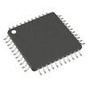
DSPIC30F4013T-30I/PT
Microchip Technology
IC MCU 16BIT 48KB FLASH 44TQFP
ADF4106BRUZ-RL
Analog Devices Inc.
IC CLK/FREQ SYNTH 16TSSOP
EL8403IS
Elantec
IC OPAMP GP 4 CIRCUIT 14SOIC
8A35001B-001AJG
Renesas Electronics America Inc
NETWORK TIMING
GRM0337U1HR90BD01D
Murata Electronics
CAP CER 0.9PF 50V U2J 0201
LT1356CS#PBF
Analog Devices Inc.
IC VOLTAGE FEEDBACK 2 CIRC 16SO
AON7280
Alpha & Omega Semiconductor Inc.
MOSFET N-CH 80V 20A/50A 8DFN
IRLI540N
Infineon Technologies
MOSFET N-CH 100V 23A TO220AB FP
VI-J6Z-MZ
Vicor Corporation
VI-J6Z-MZ 300V 2V 5A -
LMH6722MA
Texas Instruments
IC AMP CURRENT FEEDBACK 14SOIC
HZM6.8Z4MWATL-E
Renesas Electronics America Inc
TVS DIODE 3.5VWM 3MPAK
LM4041DIM7-1.2
Texas Instruments
IC VREF SHUNT 1% SC70-5
RT6200GE
Richtek USA Inc.
IC REG BUCK ADJ 600MA SOT23-6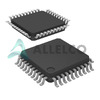
R5F21274SNFP#X6
Renesas Electronics America Inc
IC MCU 16BIT 16KB FLASH 32LQFP
1N5227B
onsemi
DIODE ZENER 3.6V 500MW DO35
12102C472JAT2A
KYOCERA AVX
CAP CER 4700PF 200V X7R 1210
PZTA64
Fairchild Semiconductor
SMALL SIGNAL BIPOLAR TRANSISTOR,
XC1765ELSO8C
AMD
IC PROM SER C-TEMP 3.3V 8-SOIC
XR88C92CJ-F
MaxLinear, Inc.
IC UART FIFO DUAL 44PLCC
RT24C2X202
Bourns, Inc.
TRIMMER 2K OHM 0.75W PC PIN SIDE
DLW31SN900SQ2L
Murata Electronics
CMC 370MA 2LN 90 OHM SMD
LMK432F476ZM-T
Taiyo Yuden
CAP CER 47UF 10V Y5V 1812
MOC207R1VM
onsemi
OPTOISO 2.5KV TRANS W/BASE 8SOIC
GRM0335C1E390JD01D
Murata Electronics
CAP CER 39PF 25V C0G/NP0 0201
SE10PG-M3/84A
Vishay General Semiconductor - Diodes Division
DIODE GEN PURP 400V 1A DO220AA
RABS15M REG
Taiwan Semiconductor Corporation
BRIDGE RECT 1P 1KV 1.5A ABS-L
PI74LPT16245AEX
Diodes Incorporated
IC TXRX NON-INVERT 3.6V 48TSSOP