
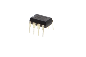
Comprehensive Guide to the 74LS74 Dual D Flip-Flop
This article explores the 74LS74 D flip-flop, a key component in sequential logic systems. It highlights the IC's bistable functionality, pin configuration, operational characteristics, and diverse applications in digital electronics. You will gain insights into its role in data storage, synchronization, and advanced system design.Catalog

Overview of 74LS74 D-Type Flip-Flop
The 74LS74 integrated circuit, a dual edge-triggered D-type flip-flop, excels in maintaining and altering data within digital electronic frameworks. It demonstrates adaptability by seamlessly integrating with diverse circuits like CMOS, TTL, and NMOS, reflecting its suitability for varied electronic landscapes. The flip-flop's design enables it to adjust outputs based on logic levels captured during low input preset conditions, showcasing its proficiency in analyzing and responding to input signals.
This flip-flop adeptly seizes and retains the D input throughout clock cycle phases. It specifically preserves the state at the precise positive edge of each clock pulse. This precision in capture is cherished in synchronous systems, where timing elevates system performance. This dependable data capture parallels the accuracy required by precision tools in timing or frequency applications, which demand unwavering consistency.
On a macro scale, one might draw parallels between the 74LS74's function in sophisticated systems and the synchronization necessary for orchestrating complex operations. Here, precise timing facilitates coherence and streamlines efficiency. The flip-flop's capability to securely store data integrity across cycles explains its extensive utility across various digital applications, including data storage in computer memory and environments.
74LS74 Pin Configuration

|
Pin No. |
Pin Symbol |
Pin Name |
Description |
|
5, 9 |
1Q / 2Q |
Output |
Output Pin of the Flip Flop |
|
6, 8 |
1Q’(bar) / 2Q’(bar) |
Complementary Output |
Inverted output pin of Flip Flop |
|
3, 11 |
1CLK / 2CLK |
Clock Input Pin |
These pins must be provided with clock pulse for the flip
flop |
|
1, 13 |
1CLR (bar) / 2CLR (bar) |
Clear Data |
Resets the flip flop by clearing its memory |
|
2, 12 |
1D / 2D |
Data Input Pin |
Input pin of the Flip Flop |
|
4, 10 |
1PRE (bar) / 2PRE (bar) |
PRE Input |
Another Input pin for Flip Flop. Also referred to as a
set pin |
|
7 |
Vss |
Ground |
Connected to the ground of the system |
|
14 |
Vdd/Vcc |
Supply Voltage |
Powers the IC typically with 5V |
Features of the 74LS74
• Operates on 2V to 15V.
• Fast 40ns signal transition time.
• Works in temperatures from 0°C to 70°C.
• Outputs up to 8mA for moderate loads.
• Dual D-type flip-flops with bipolar inputs and push-pull outputs.
• Low power use, reduced EMI.
• Ideal for digital logic, data storage, and sequential circuits.
• Requires good thermal management and proper grounding.
Applications of 74LS74
Shift Registers and Control Devices
In the landscape of shift registers, the 74LS74 shapes intricate timing sequences used for managing data streams effectively. By providing smooth data transfer and synchronization, it enhances digital circuit functionality. Its precise data handling boosts the efficacy of converting data between serial and parallel formats. Telecommunications designs frequently depend on this feature to uphold data integrity and signal precision.
Memory and Buffering Circuits
In memory architectures, the 74LS74 not only stores data bits but ensures consistency throughout processes. Its role as a buffer plays a part in executing input-output tasks while preserving signal integrity. This buffering is important to avert data loss in high-speed computing contexts.
Latching Mechanisms
The 74LS74's latching capacity enables it to securely retain information, holding importance in state retention devices. These mechanisms play a role in preserving system states during power cycles, allowing systems to restart accurately. In automotive control systems, maintaining certain states prevents malfunctions and enhances safety.
Integration in Televisions, Computers, and Networking Tools
It aids in executing varied logic operations for signal processing and display tasks. Networking tools gain from the chip's ability to manage multiple data paths simultaneously, boosting throughput and lowering latency.
Equivalents of 74LS74
• HEF40312B
Using the 74LS74 IC
The 74LS74 is a versatile D-type flip-flop known for its fast switching and low power consumption, making it ideal for synchronous data tasks. To ensure proper operation, start by confirming that the Vcc and GND pins are correctly connected to provide stable power. Reliable power connections are important to prevent issues caused by interference or irregularities in the supply. The clock input, located on Pin 3, controls the timing of data capture. When the clock receives a high signal, the flip-flop captures data. Clock signals can be sourced from microcontrollers (MCUs) or a 555 timer, depending on the timing needs of the circuit.
The reset functionality is another important feature of the 74LS74. Applying a high signal to the reset inputs clears stored data, a capability useful in systems requiring rapid data clearing. Proper placement of reset lines can optimize operations and improve overall system performance. To further enhance reliability, it’s important to address potential signal interference through effective grounding practices and strategic circuit design. These measures ensure the 74LS74 performs consistently, even in complex configurations. You can maximize the efficiency and dependability of the 74LS74 in your circuit designs. The figure below shows the 74LS74 D-type flip-flop integrated circuit connected in a configuration that uses its clock and reset inputs to manage data states, demonstrating its application in a digital logic circuit.

74LS74 D-Type Flip-Flop
|
PRE (bar) |
CLR (bar) |
CLK |
D |
Q |
Q (bar) |
|
L |
H |
X |
X |
H |
L |
|
H |
L |
X |
X |
L |
H |
|
L |
L |
X |
X |
H |
H |
|
H |
H |
H |
H |
L |
|
|
H |
H |
L |
L |
H |
|
|
H |
H |
L |
X |
Q₀ |
Q₀ (bar) |
74LS74 Connection Diagram

Advantages of D Flip-Flops
D flip-flops offer a unique advantage in digital circuit design by averting simultaneous identical input states. This aspect plays a role in averting signal races and maintaining data integrity, especially in systems where timing and sequencing elevate performance. D flip-flops ensure consistency by capturing only one input per clock cycle, thereby smoothing the data flow and minimizing potential metastability errors. For designers, the assured data flow stability provided by D flip-flops is a trusted feature to manage timing challenges that could compromise computer or network systems.
The architecture of D flip-flops provides utility as delay elements within sophisticated circuit arrangements. Utilizing gated mechanisms, they can be adjusted to impose specific delays, managing signal propagation with precision. This deliberate timing is beneficial in pipeline architectures that require data to traverse multiple stages predictably. The capability to modulate delay assists in resolving clock skew issues, which, if unattended, could hinder circuit performance.
Package for 74LS74

Conclusion
The 74LS74 D-type flip-flop is important for managing data with precision in digital electronics, ensuring reliable synchronization and storage in a variety of applications. Its versatility and efficiency in processing and retaining data make it a valuable component in creating stable and functional electronic systems. With the capacity to operate under varying conditions while maintaining signal integrity, the 74LS74 continues to be a building block in advancing electronic design and implementation. Its ongoing relevance and adaptability in new technological contexts show its importance in the field.
About us
ALLELCO LIMITED
Read more
Quick inquiry
Please send an inquiry, we will respond immediately.
Frequently Asked Questions [FAQ]
1. How many flip-flops in 7474?
The 7474 integrated circuit contains two separate D-type flip-flops, each with the ability to detect edge-trigger events. This design facilitates efficient digital signal storage and transition, refining the data handling process. Edge-triggering enhances accuracy and dependability, a subtlety often appreciated through hands-on experience in complex systems.
2. What does the triangle mean on 74LS74?
In digital electronics, the triangle represents edge-triggered clocking, aligning operations seamlessly. Coupled with it is a circle denoting active-low signaling, which aids in accurate electronic logic level readings. These symbols have proven in preventing misconstrued designs, a lesson ingrained in the minds of professionals to avert system breakdowns.
3. What is the purpose of a 74LS74?
Primarily, the 74LS74 stores binary data, allowing users to make precise alterations. This adaptability is particularly advantageous for those in system design, where assurance in adaptability and system trustworthiness is highly prized, underlining the IC's role in sophisticated computing landscapes.
4. What is the D flip flop using 7474?
Activated by edge transitions, a D flip-flop within a 7474 aligns Q outputs with input boundaries. Practical experiences shows this mechanism's contribution to robust and refined data management, for the successful operation of complex digital infrastructures.
5. How does 74LS74N work?
The 74LS74N engages its pins, enabling each flip-flop to operate independently. This independent functioning is cherished in practical applications, where a modular design strengthens system dependability and adaptability, a preference often echoed in dynamic scenarios.
6. What are the 4 types of flip-flops?
There are four main flip-flop types: Latch/Set-Reset (SR), JK, T (Toggle), and D (Delay or Data). Each serves a specialized role in data handling systems, informed by diverse practical applications where refining digital processes holds value.
7. What is the difference between D and T flip-flop?
D flip-flops capture data aligned with clock signals, whereas T flip-flops rely on T inputs to toggle states. This differentiation caters to applications demanding intricate timing and control, where thoughtful selection and integration can substantially elevate system performance.
8. What is D flip-flop truth table?
A D flip-flop truth table effectively prevents the simultaneous assertion of S and R inputs, using a gated SR configuration with an inverter to present a singular D input. In practical circuit design, this setup is adept at preventing race conditions, a common obstacle engineers strive to overcome.
9. What is the difference between latch and flip flop?
Flip-flops are edge-triggered, unlike latches which react to input level changes. Grasping this difference is beneficial for effective circuit design, as it meets unique temporal precision needs, a persistent ambition for optimizing digital systems.
Everything You Need to Know About the LM358N Operational Amplifier
on November 26th

TL082 Dual JFET Op-Amp: Pinout, Equivalents, and Applications
on November 26th
Popular Posts
-

Complex Instruction Set Computers: How They Changed Computing?
on June 14th 148402
-

USB-C Pinout and Features
on June 14th 131612
-

Using Xilinx Unified Simulation Primitives: A Comprehensive Guide to FPGA Design and Simulation
on June 14th 111884
-

Power Supply Voltages in Electronics: Meaning of VCC, VDD, VEE, VSS, and GND
on June 14th 94454
-

RJ45 Connector Guide: Pinout, Wiring, Cable Types, and Uses
on January 1th 93984
-

The Ultimate Guide to Wire Color Codes in Modern Electrical Systems
The way our electrical systems use colors isn’t just for looks. Each wire color now indicates a specific function, making it easier to identify and handle electrical components correctly during ins...on January 1th 76891
-

Quality (Q) Factor: Equations and Applications
The quality factor, or 'Q', is important when checking how well inductors and resonators work in electronic systems that use radio frequencies (RF). 'Q' measures how well a circuit minimizes energy...on January 1th 74842
-

Purge Valve Guide: Function, Symptoms, Testing, and Replacement for Optimal Engine Performance
The purge valve is a key part of a car’s system that helps keep the air clean by managing fuel vapors before they can escape into the atmosphere. This not only helps the environment by reducing pol...on January 1th 68783
-

Understanding Capacitors and Their Symbols in Circuit Diagrams
Capacitors are small parts used in almost all electronic devices. They store and release electrical energy and are found in things like power supplies, radios, and circuits that help reduce noise. ...on June 14th 58527
-

A23 Battery Specifications and Compatibility
The A23 battery is a small, cylinder-shaped battery with high voltage. Also called 23A, 23AE, or MN21, it runs at 12 volts and much higher than AA or AAA batteries. Its special design make...on January 1th 58132
HOT Part Number
-
ADAU1978WBCPZ
Analog Devices Inc.
IC ADC 24BIT 192K 40LFCSP-WQ
MIMX8MM1CVTKZAA
NXP USA Inc.
IC MPU I.MX 8M MINI SOLOLITE
REC10-2405S/H3/M
Recom Power
DC DC CONVERTER 5V 10W
SBR20100CTFP
Diodes Incorporated
DIODE ARRAY SBR 100V 10A ITO220
SN74LS640NSR
Texas Instruments
IC TRANSCEIVER INVERT 5.25V 20SO
PM8371-BI
PMC-Sierra
PM8371-BI
M2S025-FGG484
Microchip Technology
IC SOC CORTEX-M3 166MHZ 484FBGA
AT28C010-20TI
Microchip Technology
IC EEPROM 1MBIT PARALLEL 32TSOP
EP1C12F324C6N
Intel
IC FPGA 249 I/O 324FBGA
MC74VHCT373ADTRG
onsemi
IC LATCH TRANSP OCT 2ST 20-TSSOP
GBO25-12NO1
IXYS
BRIDGE RECT 1P 1.2KV 25A 4SIP
NCP302LSN20T1G
onsemi
IC SUPERVISOR 1 CHANNEL 5TSOP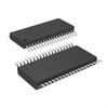
SI3210-KT
Skyworks Solutions Inc.
IC TELECOM INTERFACE 38TSSOP
ADAU1787BCBZRL
Analog Devices Inc.
4 ADC, 2 DAC LOW POWER CODEC, AU
74VHC164MTCX
onsemi
IC SHIFT REGISTER 8BIT 14TSSOP
DAN222M3T5G
onsemi
DIODE ARRAY GP 80V 100MA SOT723
DG9451EN-T1-E4
Vishay Siliconix
IC MUX 8:1 105OHM 16MINIQFN
NPX-C01767
Amphenol NovaSensor
SENSOR PRES -

AOT5B65M1
Alpha & Omega Semiconductor Inc.
IGBT 650V 5A TO220
MPC508AU
Texas Instruments
IC MUX 8:1 1.5KOHM 16SOIC
TMS320DM355DZCE135
Texas Instruments
IC DGTL MEDIA SOC 337NFBGA
EFR32BG22C112F352GM32-CR
Silicon Labs
BLUE GECKO, QFN32, SECURE BOOT W
JMK105C6225MV-F
Taiyo Yuden
CAP CER 2.2UF 6.3V X6S 0402
MAX4481AXT+T
Analog Devices Inc./Maxim Integrated
IC OPAMP GP 1 CIRCUIT SC70-6
8A35001B-001AJG
Renesas Electronics America Inc
NETWORK TIMING
ACH3218-151-TD01
TDK Corporation
FILTER LC(T) SMD
VI-JND-IY
Vicor Corporation
DC DC CONVERTER 85V 50W
2204740-1
TE Connectivity AMP Connectors
CONN SPRING SLIDING BUS 2POS PCB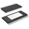
TAS5142DDVRG4
Texas Instruments
IC AMP CLSS D STER 100W 44HTSSOP
PC451J00000F
SHARP/Socle Technology
OPTOISOLATOR 3.75KV TRANS 4SMD
GRM1557U1H8R6DZ01D
Murata Electronics
CAP CER 8.6PF 50V U2J 0402
GRM2196P2A220JZ01D
Murata Electronics
CAP CER 22PF 100V P2H 0805
R5F51116ADFL#3A
Renesas Electronics America Inc
IC MCU 32BIT 256KB FLASH 48LFQFP
SN65LVDS050PWR
Texas Instruments
IC TRANSCEIVER FULL 2/2 16TSSOP
VI-J6Z-MZ
Vicor Corporation
VI-J6Z-MZ 300V 2V 5A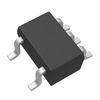
LM4041DIM7-1.2
Texas Instruments
IC VREF SHUNT 1% SC70-5 -
B32522N6684K289
EPCOS - TDK Electronics
CAP FILM 0.68UF 10% 450VDC RAD
CLA110MB1200NA
IXYS
MOD THYRISTOR DUAL 1200V SOT-227
RT6200GE
Richtek USA Inc.
IC REG BUCK ADJ 600MA SOT23-6
MAX17501GATB+T
Analog Devices Inc./Maxim Integrated
IC REG BUCK ADJ 500MA 10TDFN
PZTA64
Fairchild Semiconductor
SMALL SIGNAL BIPOLAR TRANSISTOR,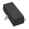
DRV5013ADEDBZRQ1
Texas Instruments
MAGNETIC SWITCH LATCH SOT23-3
HMC593LP3E
Analog Devices Inc.
IC AMP WIMAX 3.3GHZ-3.8GHZ 16QFN
74F02SCX
Fairchild Semiconductor
IC GATE NOR 4CH 2-INP 14SOIC
PE42423B-Z
pSemi
IC RF SWITCH SPDT 6GHZ 16QFN
LMK432F476ZM-T
Taiyo Yuden
CAP CER 47UF 10V Y5V 1812
MAX774ESA+
Analog Devices Inc./Maxim Integrated
IC REG CTRLR BUCK-BOOST 8SOIC
0805YD105MAT4A
KYOCERA AVX
CAP CER 1UF 16V X5R 0805
GRM155R71E103KA01J
Murata Electronics
CAP CER 10000PF 25V X7R 0402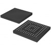
MSP430FG4616IZQWR
Texas Instruments
IC MCU 16BIT 92KB FLASH 113BGA
RABS15M REG
Taiwan Semiconductor Corporation
BRIDGE RECT 1P 1KV 1.5A ABS-L
L6470H
STMicroelectronics
IC MTR DRV BIPLR 3.3/5V 28HTSSOP
UCC2973PW
Texas Instruments
IC CCFL CNTRL 160KHZ 8TSSOP
PI74LPT16245AEX
Diodes Incorporated
IC TXRX NON-INVERT 3.6V 48TSSOP