EP1C4F400C8 FPGA: Features, Specifications, Programming and Alternatives
If you’re working with programmable logic, the EP1C4F400C8 gives you a practical balance of performance and cost. In this article, you’ll learn what this FPGA is, its key features like logic capacity, memory, and I/O options, and how its structure supports reliable design. You’ll also see its specifications, applications in systems, programming process, and how it compares to similar parts.Catalog
What is the EP1C4F400C8?
The EP1C4F400C8 is a member of Intel’s (formerly Altera’s) Cyclone FPGA family, designed as a cost-effective and reliable programmable logic solution. Built on a 0.13 µm SRAM process, this device offers moderate logic density and flexible I/O options within a compact FBGA-400 package. The Cyclone family, which includes devices like EP1C3, EP1C6, EP1C12, and EP1C20, was created to balance performance and affordability for scalable designs, allowing easy migration between density levels and packages. Known for stability and broad adoption, it remains a trusted choice in legacy designs.
Looking for EP1C4F400C8? Contact us to check current stock, lead time, and pricing.
EP1C4F400C8 CAD Models
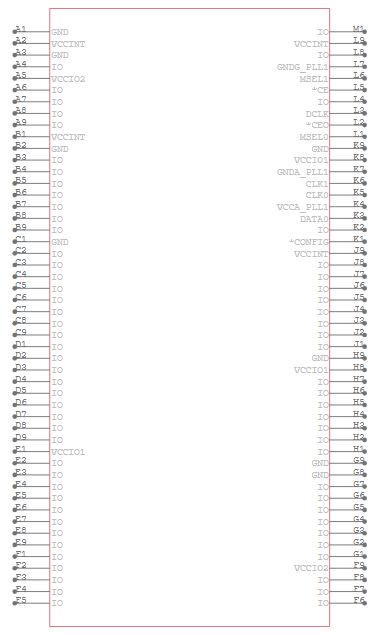
EP1C4F400C8 Symbol
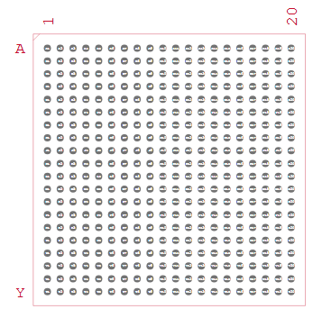
EP1C4F400C8 Footprint
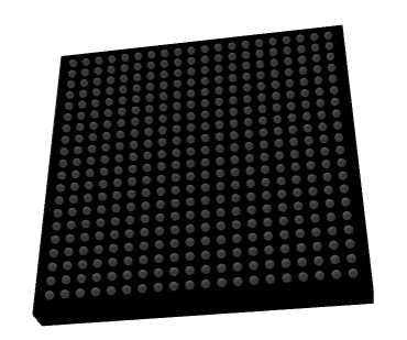
EP1C4F400C8 3D Model
EP1C4F400C8 Features
• Logic Capacity
The EP1C4F400C8 offers around 4,000 logic elements, organized into 400 Logic Array Blocks (LABs). This makes it suitable for mid-range designs that require moderate logic density while maintaining cost efficiency.
• Embedded Memory
It integrates approximately 76.5 kbits of embedded memory. This internal RAM supports data buffering, storage, and small memory functions, reducing the need for external memory components in many designs.
• High I/O Count
The device provides 301 user-configurable I/O pins in its 400-ball FBGA package. This high pin count enables rich connectivity for complex systems requiring multiple peripheral interfaces.
• Wide I/O Standards Support
It supports multiple I/O standards including LVTTL, LVCMOS, SSTL-2, SSTL-3, and differential LVDS. This flexibility allows the FPGA to interface directly with a variety of modern logic families and memory devices.
• High-Speed Differential Signaling
With LVDS support up to 640 Mbps, the FPGA handles fast data transfer requirements. This makes it practical for applications such as high-speed communication links and fast digital interfaces.
• Clock Management with PLLs
The chip integrates two Phase-Locked Loops (PLLs) and eight global clock networks. These features allow precise clock generation, multiplication, and jitter control for timing-critical applications.
• Low-Voltage Core Operation
Operating at a nominal 1.5 V core voltage, the device balances performance with lower power consumption. This voltage level was optimized for the 0.13-µm CMOS technology used in its fabrication.
• Flexible I/O Voltages
The FPGA supports I/O voltages of 1.5 V, 1.8 V, 2.5 V, and 3.3 V across different banks. This versatility enables it to interface with both legacy and modern system components.
• SRAM-Based Configuration
Like other Cyclone FPGAs, it is SRAM-based and requires reconfiguration at every power-up. This provides flexibility for updates but also necessitates an external configuration device or controller.
• Bitstream Compression Support
The EP1C4F400C8 supports compressed bitstream loading during configuration. This reduces external memory requirements and speeds up configuration times.
• PCI Compliance
It includes built-in support for PCI standards (33/66 MHz, 32/64-bit). This feature allows the device to be directly integrated into systems requiring PCI interfacing without additional bridging logic.
Cyclone LAB Structure
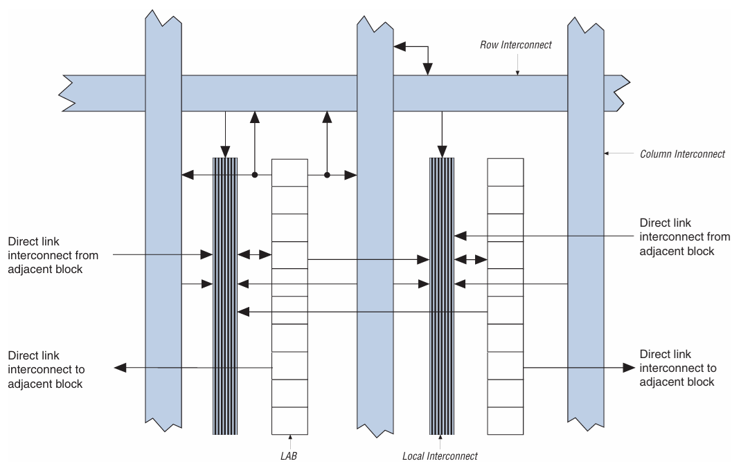
The diagram shows the Logic Array Block (LAB) structure used in Cyclone FPGAs like the EP1C4F400C8. Each LAB connects to a network of interconnects: row interconnects, column interconnects, and local interconnects, which route signals between logic elements and other blocks. Direct link interconnects provide fast, low-latency paths to adjacent LABs, improving timing performance in signal paths. This architecture is important because it balances routing flexibility with efficiency, enabling the FPGA to handle complex designs while keeping speed and area optimized.
Cyclone I/O Banks Diagram
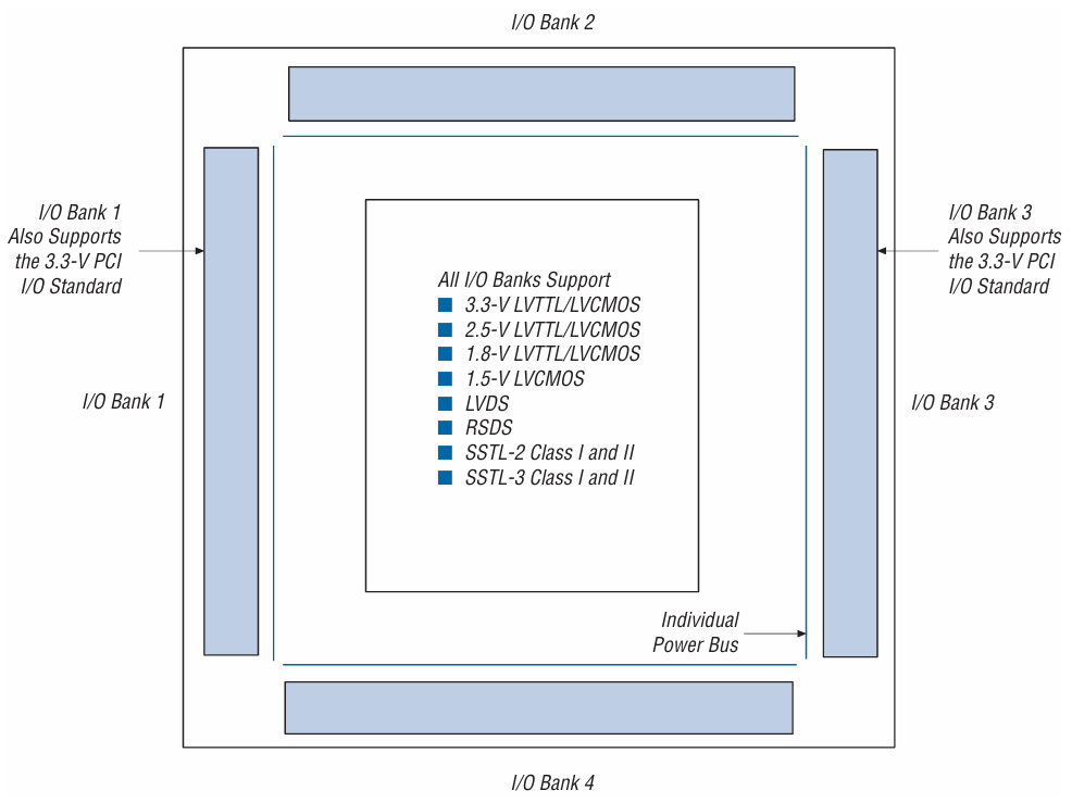
The diagram illustrates the I/O bank structure of Cyclone FPGAs such as the EP1C4F400C8. The device is divided into four I/O banks, each powered by its own supply bus, allowing to mix different voltage standards within a single FPGA. All banks support a wide range of I/O standards including LVTTL, LVCMOS, LVDS, RSDS, and SSTL, while Banks 1 and 3 also support 3.3-V PCI for compatibility with legacy systems. This flexible I/O architecture is important because it enables seamless integration with diverse external devices and interfaces, making the FPGA adaptable to various applications.
EP1C4F400C8 Specifications
|
Type |
Parameter |
|
Manufacturer |
Altera/Intel |
|
Series |
Cyclone® |
|
Packaging |
Tray |
|
Part Status |
Obsolete |
|
Number of LABs/CLBs |
400 |
|
Number of Logic Elements/Cells |
4000 |
|
Total RAM Bits |
78,336 |
|
Number of I/O |
301 |
|
Voltage – Supply |
1.425V ~ 1.575V |
|
Mounting Type |
Surface Mount |
|
Operating Temperature |
0°C ~ 85°C (TJ) |
|
Package / Case |
400-BGA |
|
Supplier Device Package |
400-FBGA (21×21) |
|
Base Product Number |
EP1C4 |
EP1C4F400C8 Applications
1. Digital Signal Processing (DSP)
The EP1C4F400C8 can be programmed to perform tasks such as filtering, FFTs, and signal modulation. Its combination of logic elements and embedded memory makes it suitable for high-speed processing. This allows it to replace traditional DSP chips with a flexible FPGA solution that can be reprogrammed for different algorithms.
2. Embedded and Control Systems
In industrial and embedded systems, this FPGA is often used to implement custom controllers, sequencers, and state machines. Its reconfigurable logic allows to tailor hardware behavior precisely to system needs. By integrating control logic inside the FPGA, the number of external components is reduced, improving reliability and lowering cost.
3. Communication and Interface Bridging
The device supports multiple I/O standards and can act as a bridge between different communication protocols. It is often used to connect PCI, LVDS, SDRAM, and other interfaces seamlessly within a system. This makes it highly useful in networking equipment, embedded controllers, and legacy-to-modern interface conversions.
4. Data Acquisition and Processing
With high I/O availability and flexible memory, the EP1C4F400C8 is well-suited for data collection systems. It can directly interface with ADCs and sensors, process the data in time, and prepare it for storage or transmission. Such applications are common in medical instruments, test equipment, and scientific measurement devices.
EP1C4F400C8 Similar Parts
|
Specification |
EP1C4F400C8 |
EP1C4F400C8N |
EP1C4F400C8NAA |
EP1C4F400C6N |
EP1C4F324C8N |
EP1C4T144C8N |
|
Manufacturer |
Altera (Intel) |
Altera (Intel) |
Altera (Intel) |
Altera (Intel) |
Altera (Intel) |
Altera (Intel) |
|
FPGA Family |
Cyclone (EP1C4) |
Cyclone (EP1C4) |
Cyclone (EP1C4) |
Cyclone (EP1C4) |
Cyclone (EP1C4) |
Cyclone (EP1C4) |
|
Logic Elements (LEs) |
4,000 |
4,000 |
4,000 |
4,000 |
4,000 |
4,000 |
|
Embedded Memory (bits) |
~76.5 kbits |
~76.5 kbits |
~76.5 kbits |
~76.5 kbits |
~76.5 kbits |
~76.5 kbits |
|
I/O Pins |
301 |
301 |
301 |
301 |
249 |
97 |
|
Package / Case |
400-FBGA |
400-FBGA |
400-FBGA |
400-FBGA |
324-FBGA |
144-TQFP |
|
Speed Grade |
C8 |
C8 |
C8 |
C6 (faster) |
C8 |
C8 |
|
Core Voltage |
1.5 V |
1.5 V |
1.5 V |
1.5 V |
1.5 V |
1.5 V |
|
Operating Temp. Range |
0°C ~ 85°C |
0°C ~ 85°C |
0°C ~ 85°C |
0°C ~ 85°C |
0°C ~ 85°C |
0°C ~ 85°C |
EP1C4F400C8 Programming Steps
Before you can use the EP1C4F400C8 FPGA, you must load your design into the device. Programming involves configuring the FPGA with a bitstream file so it knows how to behave as your intended circuit.
1. Select Configuration Scheme & Set MSEL Pins
You begin by choosing the configuration scheme that best fits your setup, such as Active Serial, Passive Serial, or JTAG. This is done by setting the MSEL pins to specific logic levels before power-up. Each mode uses different pins and protocols, so you need to confirm compatibility with your design tools and configuration memory. Making the right choice here ensures a smooth configuration process.
2. Apply Power & Initialize the Device
Next, power up the FPGA’s core and I/O rails within the specified voltage ranges. During startup, keep the nCONFIG pin low to hold the device in reset until the supply voltages are stable. Once stable, you release reset and the device signals readiness by driving the nSTATUS pin. This guarantees the FPGA is properly initialized before configuration begins.
3. Transmit the Configuration Bitstream
At this stage, you send the configuration data file (bitstream) into the FPGA using your selected scheme. In Active Serial or Passive Serial mode, the bitstream comes from an external memory device, while JTAG allows direct programming via cable. The device continuously reads in the configuration data until it’s complete. Your design software generates this bitstream to match your logic requirements.
4. Confirm Successful Configuration (CONF_DONE)
When the FPGA finishes loading, it asserts the CONF_DONE pin to show that configuration data was successfully received. At the same time, the device performs internal initialization such as clearing registers and activating I/O. If CONF_DONE fails to go high, it usually means the configuration data or setup has an error. Watching this pin is the simplest way to verify the process is complete.
5. Perform Optional In-System Reconfiguration
Finally, you have the option to update or reprogram the FPGA without removing it from the board. Using JTAG or an embedded controller, you can load a new bitstream directly, which is useful for firmware updates. This flexibility allows you to modify, debug, or upgrade your system even after deployment. It ensures your FPGA-based design can adapt over time to changing requirements.
EP1C4F400C8 Advantages and Disadvantages
Advantages
• Cost-efficient choice for mid-range designs
• High I/O count compared to similar density devices
• Flexible voltage and I/O standard support
• Backed by mature tools and documentation
• Lower power use than older FPGA generations
Disadvantages
• Obsolete with limited long-term availability
• Lower logic and memory capacity vs. modern FPGAs
• Slower operating speed and I/O performance
• Requires external memory for configuration on power-up
• Lacks advanced features like DSP blocks and high-speed transceivers
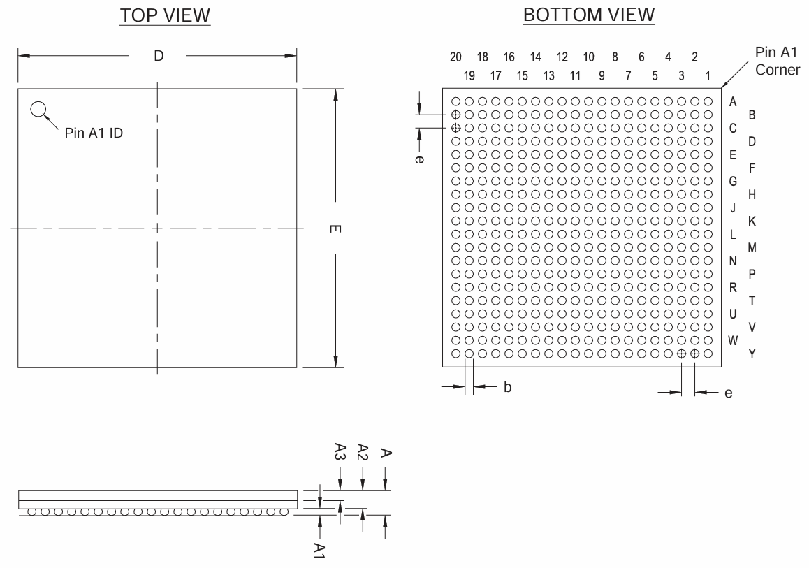
EP1C4F400C8 Packaging Dimensions
|
Type |
Parameter |
|
Package Type |
FBGA (Fine-Pitch Ball Grid Array) |
|
Ball Count |
400 |
|
Ball Pitch (e) |
1.0 mm (typical for Cyclone EP1C4F400) |
|
Ball Diameter (b) |
0.45 mm (nominal) |
|
Package Size (D × E) |
21 mm × 21 mm |
|
Package Height (A) |
2.40 mm (max) |
|
Substrate Thickness (A2) |
~0.40 mm |
|
Mold Cap Thickness (A3) |
~1.90 mm |
|
Ball Height (A1) |
0.25 mm (nominal) |
|
Pin A1 Corner |
Marked for orientation |
|
Array Layout |
20 × 20 grid (with corner balls missing) |
|
Mounting |
Surface Mount (SMD) |
EP1C4F400C8 Manufacturer
The EP1C4F400C8 was originally manufactured by Altera Corporation, a pioneer in programmable logic devices and FPGA technology. In 2015, Altera was acquired by Intel Corporation, and the product line became part of Intel’s Programmable Solutions Group (PSG). Today, Intel supports these legacy Altera devices while focusing development on newer FPGA families, ensuring continuity for existing users and advancing innovation in programmable logic.
Conclusion
The EP1C4F400C8 stands out as a cost-efficient and versatile FPGA that offers solid performance for mid-range designs. With its 4,000 logic elements, embedded memory, extensive I/O support, and compatibility with multiple voltage and interface standards, it provides flexibility across varied applications. Its architecture, programming process, and broad usability in DSP, embedded systems, and data acquisition make it a practical choice despite its legacy status. While it lacks advanced features found in newer devices and faces limited long-term availability, it remains a reliable option seeking proven solutions in scalable FPGA designs.
Datasheet PDF
EP1C4F400C8 Datasheets:
About us
ALLELCO LIMITED
Read more
Quick inquiry
Please send an inquiry, we will respond immediately.
Frequently Asked Questions [FAQ]
1. What tools are required to program the EP1C4F400C8?
You need Intel’s Quartus software (previously Altera Quartus II) along with a supported programming cable such as USB-Blaster. These tools allow you to create the bitstream and load it into the FPGA.
2. Can the EP1C4F400C8 handle PCI applications directly?
Yes, it has built-in compliance for PCI standards (33/66 MHz, 32/64-bit), making it suitable for PCI-based system integration without requiring extra bridging logic.
3. What happens if the EP1C4F400C8 fails during configuration?
If configuration fails, the CONF_DONE pin will not assert high. This usually points to an error in the bitstream file, voltage sequencing, or pin setup, and should be rechecked in your design flow.
4. Can the EP1C4F400C8 interface directly with DDR memory?
It supports several I/O standards but does not have native DDR interfaces like modern FPGAs. Additional design considerations or bridging components may be needed.
5. How does the EP1C4F400C8 compare to newer FPGAs?
Compared to modern devices, the EP1C4F400C8 has lower speed, less logic density, and fewer advanced features. However, it remains a cost-efficient choice for stable, mid-range designs where cutting-edge performance isn’t required.
EPM3256AFC256-7 CPLD Overview: Features, Pinout, Programming
on October 3th
ADG432BR Analog Switch IC: Specifications, Pinout, Alternatives and Datasheet
on October 2th
Popular Posts
-

Complex Instruction Set Computers: How They Changed Computing?
on April 17th 147713
-

USB-C Pinout and Features
on April 17th 111744
-

Using Xilinx Unified Simulation Primitives: A Comprehensive Guide to FPGA Design and Simulation
on April 17th 111324
-

Power Supply Voltages in Electronics: Meaning of VCC, VDD, VEE, VSS, and GND
on April 17th 83638
-

RJ45 Connector Guide: Pinout, Wiring, Cable Types, and Uses
on January 1th 79285
-

The Ultimate Guide to Wire Color Codes in Modern Electrical Systems
The way our electrical systems use colors isn’t just for looks. Each wire color now indicates a specific function, making it easier to identify and handle electrical components correctly during ins...on January 1th 66791
-

Quality (Q) Factor: Equations and Applications
The quality factor, or 'Q', is important when checking how well inductors and resonators work in electronic systems that use radio frequencies (RF). 'Q' measures how well a circuit minimizes energy...on January 1th 62953
-

Purge Valve Guide: Function, Symptoms, Testing, and Replacement for Optimal Engine Performance
The purge valve is a key part of a car’s system that helps keep the air clean by managing fuel vapors before they can escape into the atmosphere. This not only helps the environment by reducing pol...on January 1th 62840
-

Achieving Peak Performance with the Maximum Power Transfer Theorem
The Maximum Power Transfer Theorem explains how energy from a source, such as a battery or generator, flows to a connected load. It shows the exact condition where the load receives the most power....on January 1th 54038
-

A23 Battery Specifications and Compatibility
The A23 battery is a small, cylinder-shaped battery with high voltage. Also called 23A, 23AE, or MN21, it runs at 12 volts and much higher than AA or AAA batteries. Its special design make...on January 1th 52010
HOT Part Number
-

74438324056
Würth Elektronik
FIXED IND 5.6UH 950MA 465MOHM SM
VT2492FC-ADJ
Analog Devices Inc./Maxim Integrated
IC REG LINEAR SMD
USB4640I-HZH-03
Microchip Technology
IC INTERFACE SPECIALIZED 48QFN
NCP1400ASN25T1G
onsemi
IC REG BOOST 2.5V 80MA 5TSOP
SN74ABT241ADW
Texas Instruments
IC BUF NON-INVERT 5.5V 20SOIC
MAX4786EXS+T
Analog Devices Inc./Maxim Integrated
IC CURRENT LIMITING SC70-4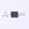
TRF7964ARHBR
Texas Instruments
IC RFID READER 13.56MHZ 32VQFN
MC7824CTG
onsemi
IC REG LINEAR 24V 1A TO220AB
TL081CD
onsemi
IC OPAMP JFET 1 CIRCUIT 8SOIC
MAX810TTRG
onsemi
IC SUPERVISOR 1 CHANNEL SOT23-3
TSX3702IPT
STMicroelectronics
IC COMPARATOR 2 CMOS 8TSSOP
C3216X7T2J333M115AC
TDK Corporation
CAP CER 0.033UF 630V X7T 1206
74AXP1T34GSH
Nexperia USA Inc.
IC TRANSLTR UNIDIRECTIONAL 6XSON
GRM0336S1E6R4DD01D
Murata Electronics
CAP CER 6.4PF 25V S2H 0201
ADS8860IDGS
Texas Instruments
IC ADC 16BIT SAR 10VSSOP
XTR104AU
Burr Brown
INSTRUMENTATION AMPLIFIER
71V65603S100BG
Renesas Electronics America Inc
IC SRAM 9MBIT PAR 119PBGA
CY2305CSXI-1T
Infineon Technologies
IC FANOUT BUFFER 8SOIC -
R5F100MJAFB#10
Renesas Electronics America Inc
IC MCU 16BIT 256KB FLASH 80LFQFP
MC10H643FNR2
onsemi
IC CLK BUFFER 1:8 80MHZ 28PLCC
R6047ENZ1C9
Rohm Semiconductor
MOSFET N-CH 600V 47A TO247
LT1950IGN#TRPBF
Analog Devices Inc.
IC REG CTRLR MULT TOP 16SSOP
LT1117CST#PBF
Analog Devices Inc.
IC REG LIN POS ADJ 800MA SOT223
AP432YL-13
Diodes Incorporated
IC VREF SHUNT ADJ 1% SOT89-3
TPS22902YFPR
Texas Instruments
IC PWR SWITCH P-CHAN 1:1 4DSBGA
SI4636DY-T1-E3
Vishay Siliconix
MOSFET N-CH 30V 17A 8SO
ICS1893AF
Renesas Electronics America Inc
IC CONTROLLER ETHERNET 48SSOP
1SMA5939BT3
onsemi
DIODE ZENER 39V 1.5W SMA
AD1849JP
Analog Devices Inc.
16-BIT SOUNDCOMM CODEC
100112DC
Texas Instruments
INVERTER/BUFFER, 100K SERIES
EC31QS03L
KYOCERA AVX
DIODE SCHOTTKY 30V 3A DO214AC
F1102NBGI8
Renesas Electronics America Inc
IC RF TO IF MIXER DUAL 36VFQFPN
V24B48H200BL2
Vicor Corporation
DC DC CONVERTER 48V 200W
EP1M120F484C6
Intel
IC FPGA 303 I/O 484FBGA
TPS76815QPWPRQ1
Texas Instruments
IC REG LINEAR 1.5V 1A 20HTSSOP
08051A270GAT4A
KYOCERA AVX
CAP CER 27PF 100V C0G/NP0 0805 -

NJW0302G
onsemi
TRANS PNP 250V 15A TO3P-3L
MUN5213DW1T1G
onsemi
TRANS PREBIAS 2NPN 50V SC88
SRP1265A-4R7M
Bourns Inc.
FIXED IND 4.7UH 13.5A 8.4MOHM SM
CHS-02TB
Nidec Components Corporation
SWITCH SLIDE DIP SPST 100MA 6V
VE-250-EY
Vicor Corporation
DC DC CONVERTER 5V 50W
142138
Amphenol RF
CONN SMB JACK STR 50 OHM PCB
74VHCT04AN
Fairchild Semiconductor
IC INVERTER 6CH 1-INP 14DIP
CFUKF455KB4X-R0
Murata Electronics
CERM FILTER 455 KHZ
2DA1213O-13
Diodes Incorporated
TRANS PNP 50V 2A SOT89-3
SN74HCT32PWRG4
Texas Instruments
IC GATE OR 4CH 2-INP 14TSSOP
TC7126ACPL
Microchip Technology
IC DRVR 7 SEG 3 1/2 DIGIT 40DIP
SP3220EBCY-L
MaxLinear, Inc.
IC TRANSCEIVER FULL 1/1 16TSSOP
LT1580CT#PBF
Linear Technology
LT1580 - 7A LOW DROPOUT HS VOLT
LM339PWR
Texas Instruments
IC COMPARATOR 4 DIFF 14TSSOP
LMV711IDBVRG4
Texas Instruments
IC OPAMP GP 1 CIRCUIT SOT23-6
CD4027BE
Texas Instruments
IC FF JK TYPE DUAL 1BIT 16DIP
TSX922IYST
STMicroelectronics
IC CMOS 2 CIRCUIT 8MINISO
IXTH26P20P
IXYS
MOSFET P-CH 200V 26A TO247