EPF6016ATC144-2N FPGA: Features, Programming, Applications, and Alternatives
This guide is all about the EPF6016ATC144-2N, a type of chip called an FPGA. It is used in digital systems that need to be flexible and easy to update. The guide explains what the chip does, how it works, its main parts and features, how to use and program it, where it can be used, and why it’s still a good choice today.Catalog
What is the EPF6016ATC144-2N?
The EPF6016ATC144-2N is a member of the FLEX 6000 FPGA family developed by Altera, now part of Intel. Built on SRAM-based reprogrammable logic, this device is engineered for flexibility in mid-density digital logic applications. It leverages the OptiFLEX architecture, which combines logic array blocks (LABs) and a high-speed interconnect matrix to deliver efficient resource utilization and fast signal routing. The EPF6016ATC144-2N supports in-system reconfiguration, making it ideal for designs requiring updates or modifications post-deployment. As part of the FLEX 6000 series, it offers a cost-effective solution for replacing traditional gate arrays while simplifying the development cycle.
Looking for EPF6016ATC144-2N? Contact us to check current stock, lead time, and pricing.
EPF6016ATC144-2N CAD Models
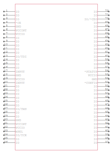
EPF6016ATC144-2N Symbol
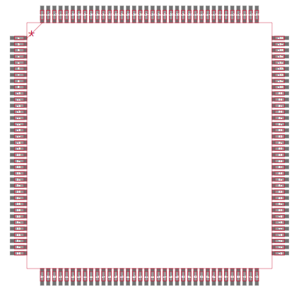
EPF6016ATC144-2N Footprint
EPF6016ATC144-2N 3D Model
EPF6016ATC144-2N Features
• Logic Capacity
The EPF6016ATC144-2N offers around 16,000 system gates, implemented using 1,320 logic elements (LEs) across 132 logic array blocks (LABs). This provides moderate complexity suitable for mid-range FPGA applications.
• I/O Pins
It supports up to 117 user-configurable I/O pins. These pins enable flexible connection to various system components and external devices.
• Core Voltage
The core operates at 3.3 V with a functional range from 3.0 V to 3.6 V. This allows compatibility with standard low-voltage digital systems.
• I/O Voltage
Its MultiVolt I/O feature supports interfacing with devices using 3.3 V or 2.5 V levels. This simplifies integration into mixed-voltage environments.
• Operating Temperature
The standard operating junction temperature range is 0 °C to +85 °C. This supports typical commercial and industrial environments.
• Supply Current
It draws approximately 5 mA during normal operation and less than 0.5 mA in standby mode. This helps conserve power in energy-conscious designs.
• Clock Speed (Speed Grade –2N)
With a –2 speed grade, it achieves internal logic frequencies up to approximately 166 MHz. This enables fast computation in signal processing or control logic.
• Architecture
Based on Altera's OptiFLEX architecture, it uses LUT-based logic with dedicated routing resources. This architecture offers high logic density and efficient performance.
• FastTrack Interconnect
The FastTrack routing grid enables low-latency signal paths and supports high-speed data transfers across logic blocks. This contributes to consistent timing and performance.
• In-Circuit Reconfiguration
It uses SRAM-based logic configuration, allowing the FPGA to be reprogrammed in-system. This supports design updates or dynamic hardware adaptation without removal.
• JTAG Boundary Scan
The device includes IEEE 1149.1-compliant JTAG boundary-scan logic. This facilitates debugging and in-system testability of boards and interconnects.
• Hot-Socketing Support
It can be safely inserted or removed while powered in 3.3 V systems. This feature is useful in modular or serviceable hardware platforms.
• Functional Testing
Each unit is fully functionally tested before shipment. This ensures quality and eliminates the need for user-defined test vectors during development.
• PCI Compatibility
The device is compatible with PCI Local Bus Revision 2.2 for 5 V operation. This allows it to be used in legacy PCI-based embedded systems.
OptiFLEX Architecture Block Diagram
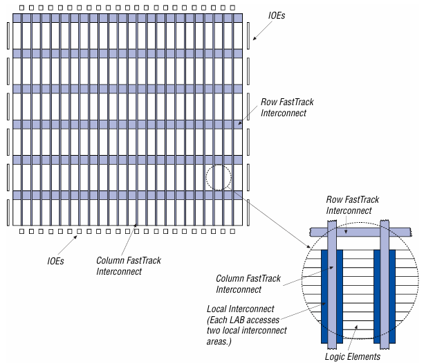
The diagram shows how the internal parts of the FPGA are organized and connected. At the center are Logic Array Blocks (LABs), these are the main building units of the chip. Each LAB contains several Logic Elements (LEs) that perform the basic digital operations, such as logic gates and flip-flops. LABs are connected by a local interconnect, which allows the logic inside each block to work together efficiently. For broader communication across the chip, the LABs link to Row and Column FastTrack Interconnects, fast signal paths that let data move quickly from one part of the chip to another with low delay. Around the outer edges of the diagram are the Input/Output Elements (IOEs). These connect the FPGA’s internal logic to external devices by converting between the chip’s logic levels and the voltage levels used by other hardware. This layout, with its modular blocks and high-speed routing paths, reflects the flexibility and performance focus of the OptiFLEX architecture.
FLEX 6000 Timing Model
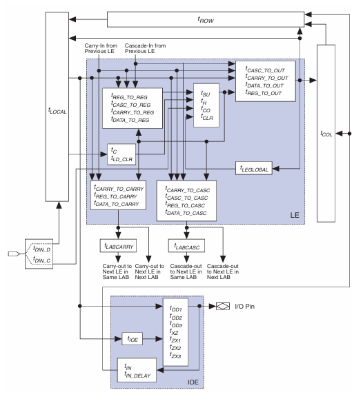
The FLEX 6000 timing model shows how signals move and are delayed as they travel through the FPGA. At the center of the model are Logic Elements (LEs), which process data and control signals with specific timing. Each LE connects to timing paths like t_DATA_TO_REG and t_REG_TO_OUT, which define how long it takes for signals to enter, be processed, and exit the logic.
Next to the LEs are special paths called LAB Carry and LAB Cascade. These allow signals to move horizontally between logic elements in the same block, supporting fast operations like additions and comparisons. These paths also have their own timing values, such as t_CARRY_TO_REG and t_CASC_TO_OUT, to measure delays during these operations.
At the bottom of the diagram, the Input/Output Elements (IOEs) handle signals going in and out of the chip. They include delay points like t_IN_DELAY, which account for variations when receiving data from external devices.
The model also includes routing paths at different levels (t_LOCAL, t_ROW, t_COL, and t_GLOBAL) each representing how far a signal travels and how much time it takes. These paths help understand and manage delays across different parts of the chip, making it easier to meet performance and timing goals.
EPF6016ATC144-2N Specifications
|
Type |
Parameter |
|
Manufacturer |
Altera/Intel |
|
Series |
FLEX 6000 |
|
Packaging |
Tray |
|
Part Status |
Obsolete |
|
Number of LABs/CLBs |
132 |
|
Number of Logic Elements/Cells |
1320 |
|
Number of I/O |
117 |
|
Number of Gates |
16000 |
|
Voltage - Supply |
3V ~ 3.6V |
|
Mounting Type |
Surface Mount |
|
Operating Temperature |
0°C ~ 85°C (TJ) |
|
Package / Case |
144-LQFP |
|
Supplier Device Package |
144-TQFP (20x20) |
|
Base Product Number |
EPF6016 |
EPF6016ATC144-2N Applications
1. Digital Signal Processing (DSP) Tasks
With 1,320 logic elements and fast interconnect, the EPF6016ATC144-2N supports the implementation of small to mid-range digital signal processing functions. It can be used to create custom FIR filters, FFT cores, or parallel arithmetic logic for signal transformation. Although it lacks dedicated DSP blocks or embedded multipliers, its general-purpose logic can handle repetitive multiply-accumulate operations suitable for embedded audio processing, sensor data filtering, and waveform shaping in control or communication systems.
2. Embedded Control and Industrial Automation
The device is well-suited for embedded control applications in industrial environments. Its ability to interface with mixed-voltage I/O (2.5 V and 3.3 V), its stable operation under standard commercial temperatures (0–85°C), and support for hot-socketing make it reliable for integration into programmable logic controllers (PLCs), motor control units, instrumentation interfaces, and general-purpose automation equipment. The reconfigurability allows for long-term product flexibility, where logic can be updated without replacing hardware.
3. Communication Protocol Bridging and Interface Logic
Thanks to its MultiVolt I/O support and efficient routing network, the EPF6016ATC144-2N can be used to implement custom communication interfaces and protocol converters. It can build UARTs, SPI controllers, or parallel bus translators to enable interaction between mismatched digital systems. Its moderate I/O count (117 GPIOs) and internal clock management also support time-sensitive signaling, making it suitable for networking equipment, legacy bus emulation, or as a glue logic element in larger data communication systems.
4. Board-Level Test, Debugging, and Validation
With built-in JTAG boundary-scan capability (IEEE 1149.1 compliant), the EPF6016ATC144-2N supports advanced board-level testing without requiring external logic probes or intrusive diagnostics. It can verify I/O connectivity, detect open or short circuits, and perform in-system checks during production or field maintenance. This feature is useful in complex multilayer PCBs or in systems where traditional access to test points is limited or impractical.
EPF6016ATC144-2N Similar Parts
|
Features |
EPF6016ATC100-1 |
EPF6016ATC100-3N |
EPF6016ATC144-3N |
|
Manufacturer |
Altera |
Intel (Altera legacy) |
Intel (Altera legacy) |
|
Family |
FLEX 6000 |
FLEX 6000 |
FLEX 6000 |
|
Logic Elements (LEs) |
1,320 |
1,320 |
1,320 |
|
Gate Count (approx.) |
16,000 |
16,000 |
16,000 |
|
Package |
100-pin TQFP |
100-pin TQFP |
144-pin TQFP |
|
User I/O Pins |
81 |
81 |
117 |
|
Speed Grade |
-1 (Standard) |
-3N (High Speed) |
-3N (High Speed) |
|
Max Clock Frequency |
Lower (typically ~100 MHz) |
Higher (up to ~166 MHz) |
Higher (up to ~166 MHz) |
|
Configuration Type |
SRAM-based |
SRAM-based |
SRAM-based |
|
Power Supply Voltage |
3.3 V |
3.3 V |
3.3 V |
|
Hot-Socketing |
Yes |
Yes |
Yes |
|
JTAG/Boundary Scan |
Yes |
Yes |
Yes |
|
Applications |
Basic logic, compact designs |
Faster control logic, compact |
High-performance systems, more I/O |
|
Availability |
Obsolete |
Obsolete |
Obsolete |
EPF6016ATC144-2N Programming Steps
1. Choose the Configuration Mode
The EPF6016ATC144-2N supports SRAM-based configuration, meaning it requires programming on every power-up. The device allows for several configuration schemes, most commonly Passive Serial (PS) and Passive Parallel Asynchronous (PPA). The configuration mode is determined by how the MSEL pin is connected. For example, when MSEL is tied low, the device expects data to be sent serially via external EEPROM (such as EPC1) or a download cable. Choosing the correct configuration method depends on the system design, EEPROM-based for automatic boot-up, or cable-based for prototyping and testing.
2. Compile the FPGA Design and Generate a Programming File
To program the FPGA, you must first create your hardware design using Intel’s Quartus or legacy MAX+PLUS II design software. After compilation, the tool generates a SOF (SRAM Object File) that represents the configured logic. This SOF must then be converted to a format compatible with your chosen configuration method:
• .rbf or .pof for EEPROM devices (e.g., EPC1).
• .ttf or .hex for microcontroller or parallel loading.
The conversion is done using the built-in File Converter utility in the design software. This step ensures that the bitstream is formatted correctly for the FPGA to interpret.
3. Program the Configuration Memory (if using EEPROM)
In applications where a serial configuration device like an EPC1 is used, the next step is to load the configuration data into the EEPROM. This is typically done using a desktop programming tool (e.g., MAX+PLUS II Programmer or Quartus Programmer). The process involves placing the EEPROM in a programming socket or connecting it in-circuit, loading the appropriate programming file (usually .pof or .rbf), and initiating the program cycle. Once programmed, the EEPROM will automatically provide the configuration data to the FPGA every time the system powers up, eliminating the need for manual reprogramming.
4. Configure Using a Download Cable (Passive Serial)
An alternative to EEPROM-based boot-up is using a download cable (such as USB-Blaster or ByteBlaster) to directly configure the FPGA. In this method, you connect the cable to your PC and the FPGA’s nCONFIG, DCLK, DATA, and CONF_DONE pins. Using the Quartus Programmer, you initiate the configuration process, which pulses nCONFIG low to begin. The tool then sends the configuration data serially through the DATA line, clocked by DCLK. The process is complete when CONF_DONE goes high, indicating successful configuration and the device’s transition to user mode.
5. Configure Using a Microcontroller (Passive Serial/Parallel)
If your system uses an embedded microcontroller, it can also act as the FPGA’s configuration master. In this setup, the microcontroller asserts nCONFIG low to reset the FPGA, then shifts the configuration bitstream through DATA while toggling DCLK. Timing requirements must be respected, data setup time before the clock and hold time afterward are good for successful configuration. The microcontroller can monitor the nSTATUS and CONF_DONE pins to detect configuration errors or confirm successful completion. This method offers full control over the configuration process and supports dynamic updates in the field.
6. Monitor Configuration Signals
During the configuration process, the FPGA provides feedback through status pins:
• nSTATUS indicates error detection; it goes low if a fault occurs (e.g., CRC error or timing violation).
• CONF_DONE goes high once all configuration bits are successfully loaded and verified.
If nSTATUS remains high and CONF_DONE transitions high at the end of the sequence, the device automatically enters user mode, where user-defined logic becomes active. This signal monitoring is important to ensure the programming process completes successfully.
7. Perform Reconfiguration When Needed
Because the EPF6016ATC144-2N is SRAM-based, it can be reconfigured at any time by toggling the nCONFIG pin low, which resets the device and restarts the configuration cycle. This feature allows for flexible system updates and changes during operation without physical replacement. The ability to reconfigure while in-circuit also supports redundancy, dynamic function swapping, or correcting bugs post-deployment. This makes the device highly suitable for applications requiring adaptability or longevity.
8. Observe Timing and Electrical Requirements
Programming the EPF6016ATC144-2N successfully also requires attention to electrical and timing constraints. The configuration clock (DCLK) must meet frequency limits (e.g., typically up to 10 MHz in standard serial modes). The device requires a short delay (about 200 ms) after power-up for the internal power-on reset to stabilize. Additionally, all configuration signals should be clean, noise-free, and properly terminated. If using hot-socketing, care must be taken to ensure signal integrity and proper sequencing of power and I/O.
EPF6016ATC144-2N Advantages
• Cost-Effective for Mid-Complexity Designs
The EPF6016ATC144-2N strikes a balance between affordability and functionality, making it ideal for designs that require more flexibility than fixed logic but don’t justify the expense or power overhead of high-end FPGAs.
• Simplified PCB Design and Integration
Compared to higher-density FPGAs that often require fine-pitch BGA packages, the EPF6016ATC144-2N comes in a standard 144-pin TQFP package. This packaging simplifies both the design and manufacturing of PCBs because it avoids the need for advanced layout tools, microvias, or costly high-layer-count boards. It also facilitates hand-soldering or basic rework, which is beneficial for smaller teams or labs with limited assembly capabilities.
• Low Risk of Obsolescence During Deployment
Due to its long-standing support in legacy industrial applications, the EPF6016ATC144-2N remains available in many secondary markets and is still widely supported in design software like Quartus II and MAX+PLUS II. For companies maintaining long-lifecycle products such as factory automation, measurement systems, or telecom modules, this ensures continued access to known-good silicon without the need to redesign hardware around newer, more complex FPGAs.
• Reliable Behavior
Unlike some newer high-performance FPGAs that operate at tight margins and are sensitive to power and temperature fluctuations, the EPF6016ATC144-2N is robust and tolerant of common environmental variations. It operates comfortably across the commercial temperature range and supports hot-socketing, which makes it reliable in modular or serviceable systems. This reliability makes it a practical choice for systems that demand consistent performance over time and under variable conditions.
• Long-Term Design Stability
In scenarios where long-term availability and design freeze are more important than cutting-edge performance, this device is a solid candidate. Once the logic is validated and the configuration file locked down, the entire system can remain unchanged for years, even decades. This is a major benefit in aerospace, transportation, and military applications where requalification of new parts is expensive or impractical.
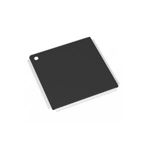
EPF6016ATC144-2N Packaging Dimensions
Package Type: TQFP-144 (Thin Quad Flat Package)
Body Size: 20 mm × 20 mm
Pin Pitch: 0.5 mm
Pin Count: 144 pins
Package Height: 1.0 mm
Lead Frame Type: Gull-wing leads on all four sides
Mounting Type: Surface-mount (SMT)
EPF6016ATC144-2N Manufacturer
The EPF6016ATC144-2N was originally manufactured by Altera Corporation, a pioneer in the development of field-programmable gate arrays (FPGAs). In 2015, Altera was acquired by Intel Corporation, and the device is now officially listed under Intel’s Programmable Solutions Group, which manages and supports Altera’s legacy FPGA product lines. Although the EPF6016ATC144-2N is part of a discontinued family, Intel remains the formal manufacturer and custodian of this device, maintaining documentation, archived support, and lifecycle notices under the Intel branding.
Conclusion
The EPF6016ATC144-2N is a flexible and dependable FPGA for many different projects. It offers a good amount of logic power, many input/output pins, and easy in-system updates. Its design supports mixed-voltage systems, fast data movement, and reprogramming without removing it from a board. It’s often used in things like control systems, signal processing, communication links, and testing equipment. With strong support, long availability, and simple packaging, it remains a smart choice who need a cost-effective and stable solution.
Datasheet PDF
EPF6016ATC144-2N Datasheets:
About us
ALLELCO LIMITED
Read more
Quick inquiry
Please send an inquiry, we will respond immediately.
Frequently Asked Questions [FAQ]
1. What tools do I need to program the EPF6016ATC144-2N today?
You can use Intel’s legacy Quartus II or MAX+PLUS II software for development and compilation. For programming, tools like the USB-Blaster cable and Quartus Programmer remain compatible for configuration.
2. Is the EPF6016ATC144-2N suitable for small production runs or prototyping?
Yes. Its TQFP-144 package makes it easy to prototype without the need for advanced assembly tools. It’s also ideal for small-scale production where low cost and flexibility are needed.
3. How does the EPF6016ATC144-2N compare to newer FPGAs in terms of performance?
While not as feature-rich as modern high-end FPGAs, the EPF6016ATC144-2N offers dependable performance for moderate logic complexity with lower power consumption and simpler integration, making it cost-effective for many applications.
4. Is it safe to hot-plug the EPF6016ATC144-2N in live systems?
Yes. This FPGA supports hot-socketing for 3.3 V systems, allowing it to be inserted or removed without powering down the host board, ideal for field service or modular hardware designs.
5. Why should I choose the EPF6016ATC144-2N over custom ASIC or CPLD solutions?
The EPF6016ATC144-2N offers faster development cycles, in-field reprogramming, and reduced upfront cost compared to ASICs. Compared to CPLDs, it provides more logic capacity and flexible routing, ideal for scalable and evolving designs.

LC5768MC-75F256C CPLD: Features, Specs, Advantages and Applications
on July 10th
Getting Started with MC7447AHX1000NB
on July 10th
Popular Posts
-

Complex Instruction Set Computers: How They Changed Computing?
on April 18th 147778
-

USB-C Pinout and Features
on April 18th 112032
-

Using Xilinx Unified Simulation Primitives: A Comprehensive Guide to FPGA Design and Simulation
on April 18th 111351
-

Power Supply Voltages in Electronics: Meaning of VCC, VDD, VEE, VSS, and GND
on April 18th 83788
-

RJ45 Connector Guide: Pinout, Wiring, Cable Types, and Uses
on January 1th 79589
-

The Ultimate Guide to Wire Color Codes in Modern Electrical Systems
The way our electrical systems use colors isn’t just for looks. Each wire color now indicates a specific function, making it easier to identify and handle electrical components correctly during ins...on January 1th 66973
-

Purge Valve Guide: Function, Symptoms, Testing, and Replacement for Optimal Engine Performance
The purge valve is a key part of a car’s system that helps keep the air clean by managing fuel vapors before they can escape into the atmosphere. This not only helps the environment by reducing pol...on January 1th 63109
-

Quality (Q) Factor: Equations and Applications
The quality factor, or 'Q', is important when checking how well inductors and resonators work in electronic systems that use radio frequencies (RF). 'Q' measures how well a circuit minimizes energy...on January 1th 63043
-

Achieving Peak Performance with the Maximum Power Transfer Theorem
The Maximum Power Transfer Theorem explains how energy from a source, such as a battery or generator, flows to a connected load. It shows the exact condition where the load receives the most power....on January 1th 54097
-

A23 Battery Specifications and Compatibility
The A23 battery is a small, cylinder-shaped battery with high voltage. Also called 23A, 23AE, or MN21, it runs at 12 volts and much higher than AA or AAA batteries. Its special design make...on January 1th 52195
HOT Part Number
-

MAX410ESA
Analog Devices Inc./Maxim Integrated
IC OPAMP GP 1 CIRCUIT 8SOIC
LTC1471CS#TRPBF
Analog Devices Inc.
IC PWR SWITCH N-CHAN 2:1 16SOIC
UDZVFHTE-179.1B
Rohm Semiconductor
DIODE ZENER 9.1V 200MW UMD2
142-0711-821
Cinch Connectivity Solutions Johnson
CONN SMA JACK STR 50OHM EDGE MNT
C3225JB1A156M230AA
TDK Corporation
CAP CER 15UF 10V JB 1210
IRLR3915TRPBF
Infineon Technologies
MOSFET N-CH 55V 30A DPAK
PS2503-1
CEL
OPTOISOLATOR 5KV TRANS 4DIP
M24308/3-4F
ITT Cannon, LLC
CONN D-SUB PLUG 37POS PNL MNT
IRFS31N20DTRLP
International Rectifier
HEXFET N-CHANNEL POWER MOSFET
DMP2108UCB6-7
Diodes Incorporated
MOSFET 8V~24V U-WLB1510-6
PI1EQX7502AZDE
Diodes Incorporated
1.05V 1-PORT/2-CHANNEL USB3.0
EMK042CG820JC-F
Taiyo Yuden
CAP CER 82PF 16V C0G/NP0 01005
LQW15AN56NG00D
Murata Electronics
FIXED IND 56NH 200MA 1.17OHM SMD
CC1206JRNPO0BN392
YAGEO
CAP CER 3900PF 100V C0G/NPO 1206
GCM188L81H333KA55D
Murata Electronics
CAP CER 0.033UF 50V X8L 0603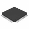
UPSD3233B-40U6
STMicroelectronics
IC MCU 8BIT 160KB FLASH 80LQFP
ATSAMG55G19B-UUT
Microchip Technology
IC MCU 32BIT 512KB FLASH 49WLCSP
MB39C316PW-G-ERE1
Infineon Technologies
IC REG 7OUT BUCK/BST/LNR 49WLCSP -
MCH3484-TL-H
onsemi
MOSFET N-CH 20V 4.5A SC70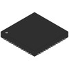
LPC2106FHN48/01
NXP USA Inc.
IC MCU 16/32B 128KB FLSH 48HVQFN
GRM152D70E224KE19D
Murata Electronics
CAP CER 0.22UF 2.5V X7T 0402
FDS8870
Fairchild Semiconductor
POWER FIELD-EFFECT TRANSISTOR, 1
PIC16LF1934-I/PT
Microchip Technology
IC MCU 8BIT 7KB FLASH 44TQFP
C3216X5R1V156M160AC
TDK Corporation
CAP CER 15UF 35V X5R 1206
73L4R47J
CTS Electronic Components
RES 0.47 OHM 5% 1/4W 1206
1206CC103JAT1A
KYOCERA AVX
CAP CER 10000PF 630V X7R 1206
CGRM4007-G
Comchip Technology
DIODE GP 1KV 1A MINI SMA/SOD123
12067A221KAT2A
KYOCERA AVX
CAP CER 220PF 500V NP0 1206
IXGH72N60C3
IXYS
IGBT 600V 75A 540W TO247AD
3214W-1-202E
Bourns Inc.
TRIMMER 2K OHM 0.25W J LEAD TOP
PM600CLA060
Powerex Inc.
MOD IPM L-SER 6PAC IPM 600V 600A
MC33063AP1
onsemi
IC REG BUCK BST ADJ 1.5A 8DIP
ADG201HSKR-REEL
Analog Devices Inc.
IC SWITCH SPST-NCX4 50OHM 16SOIC
TPS7A0328PYCHR
Texas Instruments
200-MA, NANOPOWER-IQ (200 NA), L
STR-X6756
Sanken
IC OFFLINE SWITCH FLYBACK TO3P
LMH6503MA
Texas Instruments
IC VARIABLE GAIN 1 CIRC 14SOIC -
NTA0315MC
Murata Power Solutions Inc.
DC DC CONVERTER +/-15V 1W
08051A8R2BAT2A
AVX Corporation
CAP CER 8.2PF 100V NP0 0805
S5MHE3_A/H
Vishay General Semiconductor - Diodes Division
DIODE GEN PURP 1KV 5A DO214AB
MCD700-14IO1W
IXYS
SCR THRYRISTOR 1400V WC-500
AD725AR-REEL
Analog Devices Inc.
IC ENCODER RGB TO NTSC 16-SOIC
BTS70081EPAXUMA1
Infineon Technologies
IC PWR SWTCH N-CHAN 1:1 TSDSO-14
CIH05T56NJNC
Samsung Electro-Mechanics
FIXED IND 56NH 180MA 1.4 OHM SMD
VE-2W4-EW
Vicor Corporation
DC DC CONVERTER 48V 100W
08051C332KAT2A
AVX Corporation
CAP CER 3300PF 100V X7R 0805
VI-B13-CW
Vicor Corporation
DC DC CONVERTER 24V 100W
SDA6000
RFMD
IC RF AMP 0HZ-50GHZ DIE
GRM0225C1E7R3DA03L
Murata Electronics
CAP CER 7.3PF 25V C0G/NP0 01005
71M6532D-IGT/F
Analog Devices Inc./Maxim Integrated
IC ENERGY METER 128KB 100-LQFP
AP2125K-2.8TRG1
Diodes Incorporated
IC REG LINEAR 2.8V 300MA SOT23-5
AD5160BRJ10-RL7
Analog Devices Inc.
IC DGTL POT SPI 256POS SOT23-8
CDSOT23-T24LC
Bourns Inc.
TVS DIODE 24VWM 49VC SOT23-3
C22G12
Eaton - Bussmann Electrical Division
FUSE CARTRIDGE 12A 690VAC
LI0402E300R-10
Laird-Signal Integrity Products
FERRITE BEAD 30 OHM 0402 1LN