EPM7128ATC100-10 Programmable Logic Chip Overview
Working with digital systems often means you need flexible logic that can adapt to different signal paths and control tasks. EPM7128ATC100-10 gives you a programmable logic solution that can be configured to manage timing, routing, and logic control inside electronic systems. With 128 macrocells and thousands of usable logic gates, you can build custom logic functions inside a compact device. Its surface mount package fits easily on modern circuit boards, while stable timing and flexible input and output connections help you handle many types of digital control tasks in embedded systems.Catalog
EPM7128ATC100-10 Overview
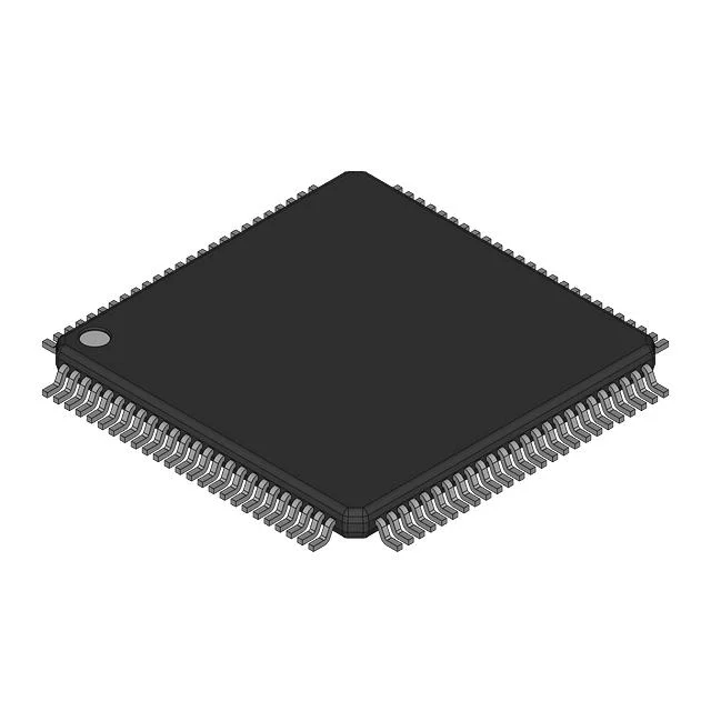
EPM7128ATC100-10 is a programmable logic device designed to implement configurable digital control functions in embedded electronic systems. The device contains 128 macrocells and roughly 2500 logic gates that allow designers to create custom logic circuits such as control logic, interface management, and state machines. Its structure organizes programmable logic within multiple logic array blocks connected through an internal routing network that distributes signals across the device. Operating from a supply range of 3 V to 3.6 V and supporting propagation delay up to 10 ns, it enables predictable logic timing. The 100 pin TQFP package supports compact surface mount installation in space constrained circuit designs.
Looking for EPM7128ATC100-10? Contact us to check current stock, lead time, and pricing.
Pin Configuration of EPM7128ATC100-10
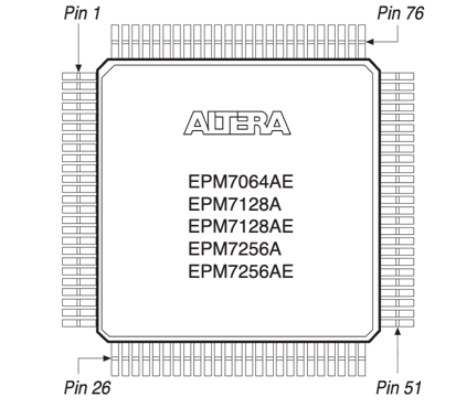
Square package layout presents a quad flat style device with metal leads extending from all four sides of the body. Pin numbers are arranged sequentially around the perimeter, beginning with pin 1 at the upper left corner and continuing along each side in order until the final pins appear on the remaining edges. Corner indicators mark key orientation points used for correct device placement on a printed circuit board. The center area contains device identification markings associated with the MAX 7000A programmable logic family. Lead spacing and symmetrical arrangement support surface mount installation and allow each external pin to connect with signal routing on the board.
Pin-Out Example of EPM7128ATC100-10
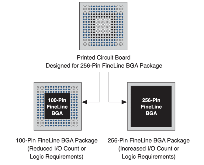
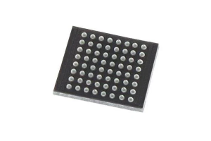
Pin arrangement demonstrates a shared printed circuit board layout that supports multiple FineLine BGA package sizes. A central board design originally prepared for a 256 pin FineLine BGA footprint is shown with a dense grid of solder ball locations. The layout allows a smaller 100 pin FineLine BGA device to be placed within the same pin field while maintaining compatible routing connections. Outer ball positions remain unused when the smaller package is installed, while the full grid is utilized for the larger device. This arrangement enables a single board design to support devices with different input output counts or logic requirements without changing the PCB layout.
Features of EPM7128ATC100-10
Programmable Logic Architecture
The device uses a macrocell based programmable logic structure that allows digital circuits to be configured after manufacturing. Each macrocell can implement combinational logic or registered logic functions, giving designers flexibility when building control paths, signal routing logic, and timing circuits. This architecture allows several discrete logic functions to be integrated into one device while maintaining predictable logic behavior.
Structured Logic Array Blocks
Internal logic resources are organized into logic array blocks that group macrocells and share routing resources. This arrangement simplifies internal signal distribution and helps maintain stable logic operation across the device. Signals can be routed between blocks through an internal interconnect network that supports complex digital logic arrangements.
Wide Input And Output Connectivity
Up to eighty four input and output pins allow the device to connect directly with multiple digital signals in an embedded system. These pins can be configured for input, output, or bidirectional operation depending on the design requirement. This flexibility allows the device to manage communication between processors, memory devices, and peripheral logic circuits.
Fast Logic Response
The device supports propagation delay of up to ten nanoseconds, enabling responsive digital logic behavior. This timing performance supports control functions that require consistent signal switching and reliable synchronization with other digital components in the system.
Electrically Reprogrammable Logic
Configuration is stored using electrically erasable programmable technology that allows the device logic to be updated when system requirements change. Designers can modify digital logic during development or system maintenance without replacing the hardware component.
Low Voltage Operation
Operation within a supply range of three volts to three point six volts allows the device to integrate with many modern digital systems. This voltage range supports stable logic levels while maintaining compatibility with common digital interface standards.
Compact Surface Mount Package
The device is provided in a one hundred pin thin quad flat package designed for surface mount assembly. The compact package footprint helps conserve board space and supports automated manufacturing processes used in modern electronic production.
Integrated Digital Control Capability
Combining programmable logic, flexible routing, and configurable input and output connections allows the device to perform various digital control tasks. It can replace multiple discrete logic circuits while maintaining stable signal behavior across embedded electronic designs.
EPM7128ATC100-10 Technical Specifications
| Product Attribute | Attribute Value |
| Manufacturer | Altera (Intel) |
| Voltage Supply - Internal | 3V ~ 3.6V |
| Supplier Device Package | 100-TQFP (14x14) |
| Series | MAX® 7000A |
| Programmable Type | EE PLD |
| Package / Case | 100-TQFP |
| Package | Bulk |
| Operating Temperature | 0°C ~ 70°C (TA) |
| Number of Macrocells | 128 |
| Number of Logic Elements/Blocks | 8 |
| Number of I/O | 84 |
| Number of Gates | 2500 |
| Mounting Type | Surface Mount |
| Delay Time tpd(1) Max | 10 ns |
| Base Product Number | EPM7128 |
| RoHs Status | RoHS non-compliant |
| Moisture Sensitivity Level (MSL) | 3 (168 Hours) |
| REACH Status | REACH Unaffected |
| ECCN | EAR99 |
| HTSUS | 8542.39.0001 |
Device Block Diagram of EPM7128ATC100-10
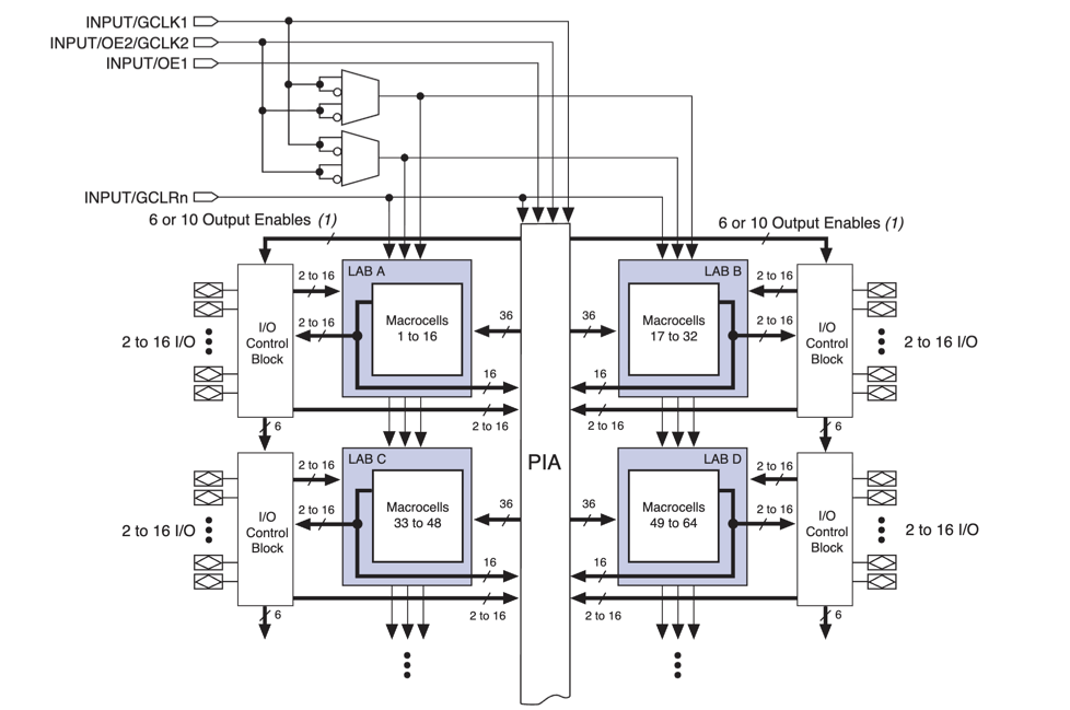
The diagram illustrates the internal logic architecture used by MAX 7000A CPLD devices such as the EPM7128ATC100-10. The structure is organized around multiple Logic Array Blocks labeled LAB A, LAB B, LAB C, and LAB D, each containing groups of macrocells that implement programmable logic functions. These macrocells support combinational logic and registered logic operations within the device. The Logic Array Blocks are connected through a central Programmable Interconnect Array that routes signals between logic sections. Each Logic Array Block connects to an I O Control Block that manages the device input and output pins. Global control signals including clock inputs, output enable signals, and global clear inputs enter from the top of the architecture and distribute control signals across the internal logic structure to coordinate device operation.
Macrocell of EPM7128ATC100-10

Logic signals enter the macrocell from the Programmable Interconnect Array through thirty six routing lines connected to the LAB local array. A product term select matrix combines these signals with up to sixteen expander product terms to create programmable logic functions. Parallel logic expanders allow additional terms from neighboring macrocells, while shared logic expanders distribute extra product terms across the logic array block to increase logic capacity. Output paths feed a programmable register that operates with global clock and clear control lines, allowing either registered or direct combinational output. A fast input select path accepts signals from an external I O pin, and a register bypass path allows the signal to pass without clocked storage. Final output signals are routed either to the I O control block for external pins or back into the Programmable Interconnect Array for internal signal routing.
Applications of EPM7128ATC100-10
Embedded System Control Logic
Programmable logic devices such as this one are often used to implement custom control logic inside embedded systems. It can coordinate timing relationships between processors, sensors, and communication devices while maintaining stable signal flow across the system.
Industrial Automation Controllers
Automation equipment frequently requires dedicated logic to manage sensors, relays, and actuator signals. The device can be programmed to handle control sequences, safety checks, and signal routing tasks used in automated machines and monitoring systems.
Telecommunications Interface Logic
Communication equipment uses programmable logic to manage signal routing between processors and interface circuits. The device can support digital switching, protocol handling, and signal conditioning that help maintain reliable communication between system components.
Consumer Electronics Control Circuits
Digital consumer products often rely on compact logic devices to coordinate internal operations. The device can manage timing, input processing, and signal control within electronic products such as multimedia equipment, home electronics, and peripheral devices.
Digital Signal Routing And Interface Management
Systems that combine multiple digital subsystems require controlled signal routing between components. The programmable logic structure allows designers to create customized routing logic that directs signals between memory, processors, and external interfaces.
State Machine Implementation
Many electronic systems rely on state machines to manage operational sequences. The device can implement these state based control structures using programmable logic paths that respond to input conditions and timing events.
Replacement For Discrete Logic Components
Several separate logic gates and control circuits can often be consolidated into one programmable device. This approach reduces board complexity while allowing logic behavior to be adjusted through configuration updates when system requirements change.
Advantages and Disadvantages of EPM7128ATC100-10
Advantages
• Flexible programmable logic allows designers to implement custom digital circuits
• Faster development cycle compared with fixed logic devices
• Compact integration of multiple logic functions within a single device
• Reliable operation with relatively low propagation delay for control logic tasks
• Supports multiple input and output connections through 84 I/O pins
• Reprogrammable architecture allows design updates during development
• Suitable for replacing several discrete logic ICs in embedded systems
Disadvantages
• Lower logic density compared with modern FPGA devices
• Limited internal resources relative to newer programmable logic families
• Restricted operating temperature range compared with industrial grade devices
• RoHS non-compliant version may limit use in some modern environmental compliance designs
EPM7128ATC100-10 Alternatives
| Part Number | Manufacturer | Key Features | Use Case/Notes |
| EPM7128ATC100-12F | Altera | MAX 7000A family CPLD with 128 macrocells and roughly 2,500 usable logic gates. Uses electrically erasable programmable logic technology and a 100-pin TQFP package with many programmable I/O connections. | Used for digital control logic, bus interface logic, and system glue logic where several digital functions must be implemented in one programmable device. |
| EPM7128ATC100-6 | Altera | Higher speed grade CPLD from the MAX 7000A architecture. Provides programmable macrocells, internal routing resources, and flexible digital input and output pins. | Suitable for timing-sensitive digital logic, interface management, and embedded control systems that require faster logic response. |
| EPM7128ATC144-10 | Altera | CPLD device using MAX 7000A architecture with nonvolatile configuration memory and a larger package that supports more I/O connections for digital system integration. | Common in industrial control boards, communication hardware, and programmable logic control tasks where additional external signals must be handled. |
About Altera (Intel)
Altera was a semiconductor company known for developing programmable logic devices used in digital systems and embedded electronics. The company specialized in field programmable gate arrays and complex programmable logic devices that allow designers to implement custom digital circuits within a single component. Its product families were widely used in communication equipment, computing platforms, industrial control systems, and consumer electronics. In 2015 the company became part of Intel, where its programmable logic technologies continue to be developed and integrated into data center, networking, and embedded computing platforms.
Conclusion
The EPM7128ATC100-10 is a programmable logic device designed to handle configurable digital control tasks in electronic systems. It combines 128 macrocells and an internal routing structure that allows you to build custom logic functions inside one compact chip. The device organizes its logic resources through logic array blocks that connect through a programmable routing network. Its pin configuration and compact TQFP package support surface mount designs used in modern circuit boards. You can use this device to manage signal routing, logic sequencing, and control functions across many digital applications. This flexibility helps simplify circuit design while keeping system behavior predictable.
About us
ALLELCO LIMITED
Read more
Quick inquiry
Please send an inquiry, we will respond immediately.
Frequently Asked Questions [FAQ]
1. What type of device is EPM7128ATC100-10?
EPM7128ATC100-10 is a complex programmable logic device that allows configurable digital logic to be implemented inside a single integrated circuit.
2. How many macrocells are available in EPM7128ATC100-10?
The device contains 128 macrocells that can implement programmable combinational or registered logic functions.
3. What package does EPM7128ATC100-10 use?
It is available in a 100 pin thin quad flat package that supports surface mount installation on printed circuit boards.
4. What are common uses for EPM7128ATC100-10?
It is commonly used for digital control logic, signal routing, interface management, and state machine implementation in embedded systems.
5. What supply voltage does EPM7128ATC100-10 require?
The device operates with an internal supply voltage range of approximately 3 volts to 3.6 volts.
Inside the S29GL256N11FFI020 NOR Flash Storage Device
on March 13th
What the EPF8282AVTC100-4 FPGA Does in Digital Systems
on March 10th
Popular Posts
-

Complex Instruction Set Computers: How They Changed Computing?
on April 18th 147762
-

USB-C Pinout and Features
on April 18th 111984
-

Using Xilinx Unified Simulation Primitives: A Comprehensive Guide to FPGA Design and Simulation
on April 18th 111351
-

Power Supply Voltages in Electronics: Meaning of VCC, VDD, VEE, VSS, and GND
on April 18th 83743
-

RJ45 Connector Guide: Pinout, Wiring, Cable Types, and Uses
on January 1th 79538
-

The Ultimate Guide to Wire Color Codes in Modern Electrical Systems
The way our electrical systems use colors isn’t just for looks. Each wire color now indicates a specific function, making it easier to identify and handle electrical components correctly during ins...on January 1th 66948
-

Purge Valve Guide: Function, Symptoms, Testing, and Replacement for Optimal Engine Performance
The purge valve is a key part of a car’s system that helps keep the air clean by managing fuel vapors before they can escape into the atmosphere. This not only helps the environment by reducing pol...on January 1th 63087
-

Quality (Q) Factor: Equations and Applications
The quality factor, or 'Q', is important when checking how well inductors and resonators work in electronic systems that use radio frequencies (RF). 'Q' measures how well a circuit minimizes energy...on January 1th 63028
-

Achieving Peak Performance with the Maximum Power Transfer Theorem
The Maximum Power Transfer Theorem explains how energy from a source, such as a battery or generator, flows to a connected load. It shows the exact condition where the load receives the most power....on January 1th 54092
-

A23 Battery Specifications and Compatibility
The A23 battery is a small, cylinder-shaped battery with high voltage. Also called 23A, 23AE, or MN21, it runs at 12 volts and much higher than AA or AAA batteries. Its special design make...on January 1th 52171
HOT Part Number
-

MC74F174DR2
onsemi
FLIP FLOP D TYPE BUS INTERFACE P
RT9173GS
Richtek USA Inc.
IC REG CONV DDR 1OUT 8SOP
PIC16F913-I/SS
Microchip Technology
IC MCU 8BIT 7KB FLASH 28SSOP
ADUM240E1BRWZ
Analog Devices Inc.
DGTL ISO 5000VRMS 4CH GP 16SOIC
VLMK20J2L1-GS08
Vishay Semiconductor Opto Division
LED AMBER CLEAR SMD MINILED SMD
2SAR544PT100
Rohm Semiconductor
TRANS PNP 80V 2.5A MPT3
SMCJ75CA-E3/57T
Vishay General Semiconductor - Diodes Division
TVS DIODE 75VWM 121VC DO214AB
ISL9444IRZ-T7A
Renesas Electronics America Inc
IC REG CTRLR BUCK 40QFN
ACPL-T350-000E
Broadcom Limited
OPTOISO 3.75KV 1CH GATE DVR 8DIP
813N252CKI-02LF
Renesas Electronics America Inc
IC JITTER ATTENUATOR 32VFQFPN
MB9BF166MPMC-G-JNE2
Cypress Semiconductor
IC MCU 32BIT 544KB FLASH 80LQFP
HFA08TA60C
Vishay General Semiconductor - Diodes Division
DIODE ARRAY GP 600V 4A TO220AB
GRM0335C1E6R1CD01D
Murata Electronics
CAP CER 6.1PF 25V C0G/NP0 0201
SN74ACT04PWR
Texas Instruments
IC INVERTER 6CH 1-INP 14TSSOP
TLC3578IPWR
Texas Instruments
IC ADC 14BIT SAR 24TSSOP
ADG202AKRZ-REEL7
Analog Devices Inc.
IC SWITCH SPST-NOX4 90OHM 16SOIC
GD25Q80EEIGR
GigaDevice Semiconductor (HK) Limited
IC FLASH 8MBIT SPI/QUAD 8USON
C0603C0G1E101K030BA
TDK Corporation
CAP CER 100PF 25V C0G 0201 -

IS62WV12816EBLL-45TLI
ISSI, Integrated Silicon Solution Inc
IC SRAM 2MBIT PARALLEL 44TSOP II
Q6010LT
Littelfuse Inc.
TRIAC INT TRIGGER 600V 10A TO220
PD130FG80
SanRex Corporation
THYRISTOR MODULE 800V 130A
MAX4451EKA-T
Analog Devices Inc./Maxim Integrated
IC OPAMP VFB 2 CIRCUIT SOT23-8
MT41J256M8DA-107:K
Micron Technology Inc.
IC DRAM 2GBIT PAR 78FBGA
SMBD1488LT1G
onsemi
SS SOT23 SWCH DIO SPCL
OPA191IDGKR
Texas Instruments
IC OPAMP GP 1 CIRCUIT 8VSSOP
CMP402GSZ
Analog Devices Inc.
IC COMPARATOR 4 GEN PUR 16SOIC
MAX11201BEUB+
Analog Devices Inc./Maxim Integrated
IC ADC 24BIT SIGMA-DELTA 10UMAX
1SR154-600TE25
Rohm Semiconductor
DIODE GEN PURP 600V 1A PMDS
S558-5500-12-F
Bel Fuse Inc.
PULSE XFMR 1 CT:1CT TX/RX 350UH
BTS436L2
Infineon Technologies
IC PWR SWITCH N-CHAN 1:1 TO220-5
CGA6M3X7R2E224K200AA
TDK Corporation
CAP CER 0.22UF 250V X7R 1210
ATTINY43U-SU
Microchip Technology
IC MCU 8BIT 4KB FLASH 20SOIC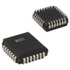
SY10E104JY
Microchip Technology
IC GATE AND/NAND QUINT 28-PLCC
TLV2442ID
Texas Instruments
IC CMOS 2 CIRCUIT 8SOIC
TDA7786
STMicroelectronics
RF RECEIVER AM/FM/WB 64LQFP
CL10C6R8CB8NNWC
Samsung Electro-Mechanics
CAP CER 6.8PF 50V C0G/NP0 0603 -

DCV012415DP
Burr Brown
DC DC CONVERTER +/-15V 1W
AFE5851IRGCT
Texas Instruments
IC AFE 16 CHAN 12BIT 64VQFN
MAX8215EPD+
Analog Devices Inc./Maxim Integrated
IC SUPERVISOR 5 CHANNEL 14DIP
CL21B103KC65PNC
Samsung Electro-Mechanics
CAP CER 10000PF 100V X7R 0805
MP2481DH-LF-P
Monolithic Power Systems Inc.
IC LED DRVR RGLTR PWM 1.2A 8MSOP
CM100DY-24H
Powerex Inc.
IGBT MOD 1200V 100A 780W
MA3Z7920GL
Panasonic Electronic Components
DIODE SCHOTT 30V 100MA SMINI3-F2
AQV225NAX
Panasonic Electric Works
SSR RELAY SPST-NO 150MA 0-80V
HCPL0600
onsemi
OPTOISO 3.75KV OPN COLLECTOR 8SO
ATSAMD21G16B-MU
Microchip Technology
IC MCU 32BIT 64KB FLASH 48QFN
TLC274CNSR
Texas Instruments
IC OPAMP GP 4 CIRCUIT 14SO
AD5242BRUZ10
Analog Devices Inc.
IC DGT POT 10KOHM 256TAP 16TSSOP
CDRH4D28NP-330NC
Sumida America Components Inc.
FIXED IND 33UH 560MA 331.3 MOHM
BSD235NH6327XTSA1
Infineon Technologies
MOSFET 2N-CH 20V 0.95A SOT363
1N1126A
Solid State Inc.
DIODE GEN PURP 400V 12A DO4
STM32F107VCT6
STMicroelectronics
IC MCU 32BIT 256KB FLASH 100LQFP
IHLP2525CZERR10M07
Vishay Dale
FIXED IND 100NH 32.5A 1.3MOHM SM
2SCR554RTL
Rohm Semiconductor
TRANS NPN 80V 1.5A TSMT3