EPM7160ELC84-15: Datasheet, Features, Pinout, Programming and Applications
This guide is all about the EPM7160ELC84-15, a special chip that helps build custom digital logic circuits. You can program it using a JTAG connection, and even update it while it's already installed in your system. It also has security features to protect your design. This article explains everything about the chip, including its pin layout, features, uses, and how to program it. Whether you're working on machines, cars, or network equipment, this guide helps you understand why this chip is useful.Catalog
EPM7160ELC84-15 Overview
The EPM7160ELC84-15 is part of Intel's MAX 7000 series of CPLDs, which utilize Altera's advanced second-generation MAX architecture. These devices, fabricated with high-end CMOS technology, are tailored for high-density and high-performance digital logic circuit implementations. This model features 160 macrocells and provides roughly 3,200 usable gates, accommodating the needs of complex digital systems. It operates on a 5V supply, with a typical pin-to-pin delay of 15 ns, allowing for counter speeds up to 175.4 MHz, ensuring rapid signal processing and efficient system performance. This CPLD supports both in-system programming and reprogramming via an integrated JTAG interface, which is compliant with IEEE Std. 1149.1, enhancing flexibility and ease of updates after installation. It also offers a security bit feature to prevent unauthorized copying of configuration data, a valuable addition for protecting intellectual property.
If you're looking to secure everything your business needs, now’s the perfect time to place a bulk order with us. We’re ready to help you save time, cut costs, and get exactly what you need.
EPM7160ELC84-15 Pinout Diagram
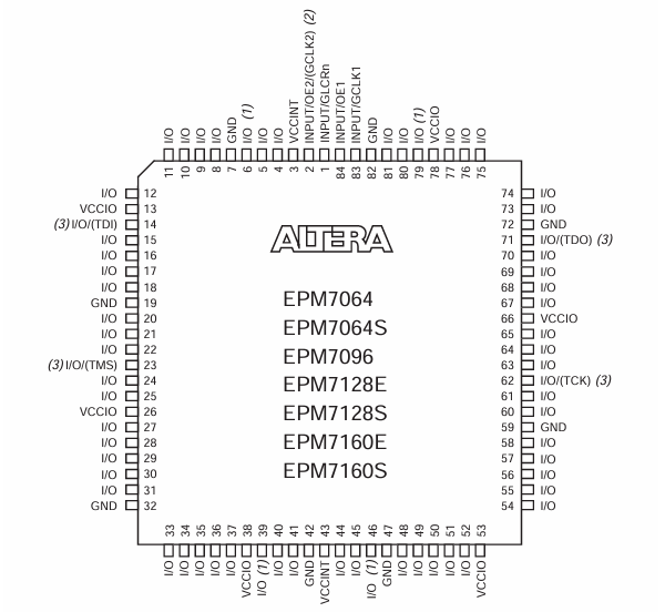
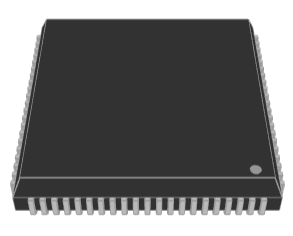
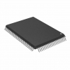
The pinout diagram for the EPM7160ELC84-15 device illustrates the physical layout and functionality of its 84 pins in a PLCC (Plastic Leaded Chip Carrier) package. The diagram shows a square configuration, where each pin is assigned a specific label that indicates its function, such as I/O (input/output), GND (ground), or VCCIO (supply voltage for I/O). Pins labeled as I/O represent configurable digital input or output lines, which are used to interface with other devices in a circuit. VCCIO pins supply voltage to the I/O banks, and GND pins provide the ground reference. Special function pins include TDI, TDO, TMS, and TCK, which are used for JTAG programming and boundary scan testing. Additionally, pins like INPUT1/CLK1 and INPUT2/CLK2 are designated clock or control signal inputs for internal logic timing.
EPM7160ELC84-15 CAD Models
EPM7160ELC84-15 Symbol
EPM7160ELC84-15 Footprint
EPM7160ELC84-15 3D Model
EPM7160ELC84-15 Features
• High-Density Logic: The EPM7160ELC84-15 offers 160 macrocells and approximately 3,200 usable gates, making it highly suitable for complex digital designs. This density allows for the integration of multiple functions into a single device, facilitating more compact and efficient circuit designs.
• Fast Performance: With a maximum propagation delay of 15 ns and the ability to support operating frequencies up to 100 MHz, this CPLD ensures rapid signal processing and high-speed performance for time-sensitive applications.
• In-System Programmability (ISP): Featuring a built-in IEEE Std. 1149.1 (JTAG) interface, the device supports in-system programming. This capability allows for the device to be programmed and reprogrammed post-installation, providing flexibility for updates and functionality changes without the need for physical replacement.
• MultiVolt™ I/O Interface: The MultiVolt I/O interface supports various operating voltages, making the CPLD compatible with 5.0 V, 3.3 V, and 2.5 V logic levels. This feature enables the device to be used in mixed-voltage systems, enhancing its adaptability to different electronic environments.
• Flexible I/O Configuration: It provides 64 programmable I/O pins that offer versatile interfacing options. This flexibility is important for applications requiring a variety of input/output configurations, supporting a broad range of connectivity and functionality.
• EEPROM-Based Memory: Utilizing EEPROM technology for configuration storage, the CPLD can be reprogrammed up to 100 times. This non-volatile memory ensures that the device retains its configuration even after power cycles for reliability and ease of maintenance.
• Security Features: The device includes a security bit that prevents unauthorized access to the programmed logic, protecting intellectual property and preventing tampering, which is good for applications in security-sensitive environments.
EPM7160ELC84-15 Block Diagram
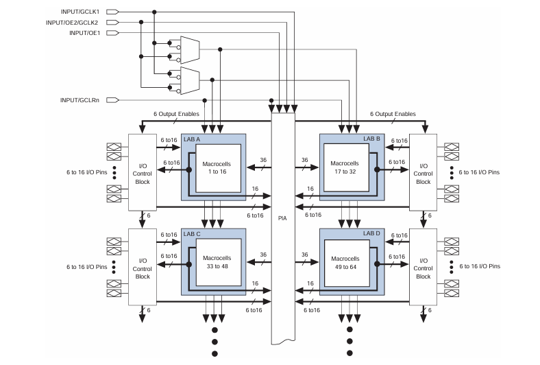
The block diagram of the EPM7160ELC84-15, represents a well-structured internal architecture composed of four Logic Array Blocks (LABs) labeled A, B, C, and D. Each LAB contains 16 macrocells, making a total of 64 macrocells, which are the building units for creating logic functions. These macrocells can implement combinational or registered logic using programmable interconnects and control signals. At the center, the Programmable Interconnect Array (PIA) serves as the communication backbone, enabling flexible routing of signals between LABs and I/O pins. Each LAB connects to the PIA with 36 input lines and 16 output lines, ensuring a high degree of logic interconnectivity. Around the periphery, I/O Control Blocks manage input and output signals, offering between 6 to 16 I/O pins per side, which interface directly with the external system. It also shows global control signals like clock (GCLK1, GCLK2), output enable (OE1), and clear (GCLRn) distributed to all LABs for synchronized and centralized logic control. These signals can be routed through multiplexers to provide design flexibility and efficiency.
EPM7160ELC84-15 Specifications
|
Type |
Parameter |
|
Manufacturer |
Altera/Intel |
|
Series |
MAX® 7000 |
|
Packaging |
Tube |
|
Part Status |
Obsolete |
|
Programmable Type |
EE PLD |
|
Delay Time tpd(1) Max |
15 ns |
|
Voltage Supply - Internal |
4.75V ~ 5.25V |
|
Number of Logic Elements/Blocks |
10 |
|
Number of Macrocells |
160 |
|
Number of Gates |
3200 |
|
Number of I/O |
64 |
|
Operating Temperature |
0°C ~ 70°C (TA) |
|
Mounting Type |
Surface Mount |
|
Package / Case |
84-LCC (J-Lead) |
|
Supplier Device Package |
84-PLCC (29.31x29.31) |
|
Base Product Number |
EPM7160 |
EPM7160ELC84-15 Applications
Industrial Automation
In the industrial automation, the EPM7160ELC84-15 is utilized to control logic within programmable logic controllers (PLCs), motor controllers, and sensor interfaces. Its ability to handle complex logic operations and fast I/O switching makes it ideal for automation tasks that require precise control and timing.
Embedded Systems
This CPLD is useful in embedded systems where space and power efficiency are important. It finds applications in robotics, Internet of Things (IoT) devices, and consumer electronics, where its programmability allows for customization and adaptability to specific functional requirements.
Telecommunications
The device is employed in telecommunications equipment such as routers and switches for managing timing, data routing, and protocol handling. Its high-speed performance and ability to operate at different voltage levels make it suitable for network infrastructure that demands reliability and high data throughput.
Automotive Electronics
Within the automotive sector, the EPM7160ELC84-15 supports applications in infotainment systems, body control modules, and engine management units. The CPLD's robustness and support for a wide range of input/output voltages allow it to perform reliably in the demanding conditions of automotive environments.
Medical Devices
The CPLD is also applied in medical device technology, particularly in diagnostic equipment and patient monitoring systems. Its security features and stable operation under various environmental conditions ensure that it can handle sensitive and healthcare applications securely and efficiently.
EPM7160ELC84-15 Similar Parts
EPM7160ELC84-15 Programming Steps
Programming the EPM7160ELC84-15, a CPLD from Intel's MAX 7000 series, involves a structured process to ensure that the device functions according to specifications. Here are the steps involved in programming this CPLD:
1. Design Entry: Start by using a hardware description language (HDL) such as VHDL or Verilog, or a graphical schematic capture tool to create your digital logic design. This initial step lays the foundation for the functionality you want to implement in the CPLD. Employ design software compatible with the MAX 7000 series, such as Altera's Quartus II or MAX+PLUS II, which provides tools for coding, compiling, and simulating your design.
2. Compilation and Simulation: Compile your design to translate the HDL code or schematic into a binary format that the CPLD can execute. This step also checks for any syntax errors and ensures that the logic meets design requirements. Simulate the compiled design to validate its functionality. This involves running test cases against the design to verify its logic and timing, ensuring it behaves as expected before it is programmed onto the physical device.
3. Programming Hardware Setup: Connect the EPM7160ELC84-15 to appropriate programming hardware. This could involve setting up a JTAG interface with devices such as the ByteBlasterMV, MasterBlaster, or USB-Blaster. Make sure the CPLD is properly powered and set up in the correct configuration mode for programming, typically using a 5.0 V power supply.
4. Programming Process: Open the programming software (like Quartus II Programmer) and configure it to recognize the EPM7160ELC84-15 via the JTAG interface. Load the appropriate programming file (.pof or .sof) into the software. These files contain the compiled design data necessary to configure the CPLD. Execute the programming command within the software to transfer the design to the CPLD. Monitor the process for any errors and confirm successful programming completion.
5. Verification: Once programming is complete, carry out a verification process to ensure that the CPLD operates correctly within its intended application. This might include conducting boundary-scan tests or functionality tests within the actual system where the CPLD is implemented. Verify that all functionalities are performed as designed and that the device interacts correctly with other components in the system.
EPM7160ELC84-15 Advantages
Cost-Effectiveness
The EPM7160ELC84-15 is a cost-effective solution for needing complex logic capabilities without the high price tag associated with newer CPLDs or FPGAs. This makes it attractive for budget-sensitive projects and for educational or small-scale industrial applications.
Non-Volatile Configuration
Utilizing EEPROM technology, the EPM7160ELC84-15 retains its programmed configuration even when the power is turned off. This non-volatility ensures device reliability and consistency in performance across power cycles, eliminating the need for external non-volatile memory components.
Wide Operating Voltage Range
The device supports a wide operating voltage range of 4.75 V to 5.25 V, accommodating varying power supplies and ensuring compatibility with both older and newer system designs. This versatility is beneficial in mixed-voltage environments where system components may not share the same standard voltage levels.
Reliable Performance
The device offers reliable performance with a propagation delay of 15 ns and support for operating frequencies up to 100 MHz. This ensures timely and efficient processing of logic operations, making it suitable for time-sensitive applications in telecommunications, automotive electronics, and industrial control systems.
EPM7160ELC84-15 Packaging Dimensions
Package Outline Dimension Table
|
Symbol |
Inches |
||
|
Min. |
Nom. |
Max. |
|
|
A |
0.165 |
0.172 |
0.18 |
|
A1 |
0.02 |
— |
— |
|
A2 |
0.150 TYP |
||
|
D |
1.185 |
1.190 |
1.195 |
|
D1 |
1.150 |
1.154 |
1.158 |
|
D2 |
1.082 |
1.110 |
1.138 |
|
E |
1.185 |
1.190 |
1.195 |
|
E1 |
1.150 |
1.154 |
1.158 |
|
E2 |
1.082 |
1.110 |
1.138 |
|
b |
0.013 |
— |
0.021 |
|
c |
0.008 TYP |
||
|
e |
0.050 TYP |
||
Package Outline
EPM7160ELC84-15 Manufacturer
The EPM7160ELC84-15 is manufactured by Intel Corporation, a global leader in semiconductor technology. Originally developed by Altera, this CPLD became part of Intel's product portfolio following its acquisition of Altera in 2015. Since then, Intel has continued to support the MAX 7000 series, including the EPM7160ELC84-15, under its Programmable Solutions Group. Intel’s stewardship ensures the device benefits from their advanced manufacturing standards, long-term reliability, and documentation support. Though now classified as obsolete, Intel's legacy in programmable logic devices like the EPM7160ELC84-15 continues to serve in legacy systems and specialized applications worldwide.
Conclusion
The EPM7160ELC84-15 stands as a highly capable CPLD tailored for engineers and system designers seeking cost-effective logic integration with flexible programmability. Its EEPROM-based memory, fast propagation delay, and compatibility with multiple voltage levels make it a strong fit for diverse electronic environments. Backed by Intel’s manufacturing legacy and built with features like MultiVolt I/O and JTAG compliance, the device continues to serve in legacy and specialized systems despite its obsolescence. Whether you’re working in industrial automation, embedded applications, or telecom infrastructure, the EPM7160ELC84-15 delivers reliable performance and long-term value.
Datasheet PDF
EPM7160ELC84-15 Datasheets:
Cylindrical Battery Holders.pdf
About us
ALLELCO LIMITED
Read more
Quick inquiry
Please send an inquiry, we will respond immediately.
Frequently Asked Questions [FAQ]
1. What’s the difference between the EPM7160ELC84-15 and newer CPLDs or FPGAs?
The EPM7160ELC84-15 is ideal for simpler or cost-sensitive applications because it's EEPROM-based and doesn’t require external configuration memory. Newer CPLDs or FPGAs may offer more logic capacity, faster performance, or advanced features, but often at a higher cost and complexity. If your design doesn’t need high-end resources, this device is a more efficient choice.
2. What software do I need to program the EPM7160ELC84-15?
You can use Altera MAX+PLUS II or Intel Quartus II software to design, compile, simulate, and program the EPM7160ELC84-15. These tools support older MAX 7000 series CPLDs and offer both schematic and HDL-based design options.
3. How many times can I reprogram the EPM7160ELC84-15?
The EPM7160ELC84-15 can be reprogrammed up to 100 times thanks to its EEPROM technology. This allows for updates and modifications during prototyping and even after deployment, offering long-term flexibility.
4. Does the EPM7160ELC84-15 support mixed voltage logic levels?
Yes, it supports MultiVolt™ I/O, meaning it can interface with devices operating at 5V, 3.3V, or even 2.5V, making it adaptable to different voltage environments and helping it integrate into mixed-technology systems.
5. Can I use a USB-Blaster for programming this CPLD?
Yes, USB-Blaster, ByteBlasterMV, and MasterBlaster are compatible programming tools that connect via JTAG to the EPM7160ELC84-15 for in-system programming (ISP).

What You Need to Know About the AD9984AKSTZ-170
on April 18th
What Capacitors Do in Electronic Circuits
on April 17th
Popular Posts
-

Complex Instruction Set Computers: How They Changed Computing?
on April 17th 147721
-

USB-C Pinout and Features
on April 17th 111782
-

Using Xilinx Unified Simulation Primitives: A Comprehensive Guide to FPGA Design and Simulation
on April 17th 111328
-

Power Supply Voltages in Electronics: Meaning of VCC, VDD, VEE, VSS, and GND
on April 17th 83649
-

RJ45 Connector Guide: Pinout, Wiring, Cable Types, and Uses
on January 1th 79346
-

The Ultimate Guide to Wire Color Codes in Modern Electrical Systems
The way our electrical systems use colors isn’t just for looks. Each wire color now indicates a specific function, making it easier to identify and handle electrical components correctly during ins...on January 1th 66806
-

Quality (Q) Factor: Equations and Applications
The quality factor, or 'Q', is important when checking how well inductors and resonators work in electronic systems that use radio frequencies (RF). 'Q' measures how well a circuit minimizes energy...on January 1th 62965
-

Purge Valve Guide: Function, Symptoms, Testing, and Replacement for Optimal Engine Performance
The purge valve is a key part of a car’s system that helps keep the air clean by managing fuel vapors before they can escape into the atmosphere. This not only helps the environment by reducing pol...on January 1th 62855
-

Achieving Peak Performance with the Maximum Power Transfer Theorem
The Maximum Power Transfer Theorem explains how energy from a source, such as a battery or generator, flows to a connected load. It shows the exact condition where the load receives the most power....on January 1th 54049
-

A23 Battery Specifications and Compatibility
The A23 battery is a small, cylinder-shaped battery with high voltage. Also called 23A, 23AE, or MN21, it runs at 12 volts and much higher than AA or AAA batteries. Its special design make...on January 1th 52032
HOT Part Number
-
CY7C1347G-133AXCT
Infineon Technologies
IC SRAM 4.5MBIT PAR 100TQFP
MAX8606ETD+T
Analog Devices Inc./Maxim Integrated
IC BATT CHG LI-ION 1CELL 14TDFN
DSPIC33EP128MC204-I/PT
Microchip Technology
IC MCU 16BIT 128KB FLASH 44TQFP
CC1206JRNPOABN560
YAGEO
CAP CER 56PF 200V C0G/NPO 1206
AGL250V2-CSG196I
Microchip Technology
IC FPGA 143 I/O 196CSP
NE5517N
onsemi
IC OPAMP TRANSCOND 2 CIRC 16DIP
CY7C1049GN30-10ZSXIT
Infineon Technologies
IC SRAM 4MBIT PARALLEL 44TSOP II
SN74HC4851DR
Texas Instruments
IC MUX 8:1 195OHM 16SOIC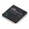
CS47048C-CQZ
Cirrus Logic Inc.
IC AUDIO SOC SGL 32BIT 100-LQFP
LT3598EFE#TRPBF
Analog Devices Inc.
IC LED DRV RGLTR PWM 24TSSOP
SN74S112AN
Texas Instruments
IC FF JK TYPE DUAL 1BIT 16DIP
MRF6S18060NR1
NXP USA Inc.
FET RF 68V 1.99GHZ TO270-4
CY14B256K-SP35XI
Infineon Technologies
IC NVSRAM 256KBIT PAR 48SSOP
TLV2450CDBVRG4
Texas Instruments
IC OPAMP GP 1 CIRCUIT SOT23-6
TSB43DA42AZHC
Texas Instruments
IC PHY/LINK LAYER CTRLR 196-BGA
LT1995CMS#PBF
Analog Devices Inc.
IC OPAMP PGA 1 CIRCUIT 10MSOP
ESD241B1W0201E6327XTSA1
Infineon Technologies
TVS DIODE 3.3VWM 6VC WLL-2-3
LT8640SIV#PBF
Analog Devices Inc.
IC REG BUCK ADJUSTABLE 6A 24LQFN -

RT1206BRD0711RL
YAGEO
RES SMD 11 OHM 0.1% 1/4W 1206
TS4990IQT
STMicroelectronics
IC AMP CLASS AB MONO 1.2W 8DFN
IHLP2525CZER2R2M01
Vishay Dale
FIXED IND 2.2UH 8A 20 MOHM SMD
EP3SE50F484C4N
Intel
IC FPGA 296 I/O 484FBGA
08055U6R8BAT2A
KYOCERA AVX
CAP CER 6.8PF 50V NP0 0805
XF2B-3945-31A
Omron Electronics Inc-EMC Div
CONN FPC 39POS 0.3MM R/A
FZT704TA
Diodes Incorporated
TRANS PNP HG 100V 1500MA SOT-223
NDD05N50ZT4G
onsemi
MOSFET N-CH 500V 4.7A DPAK
ADUM2400BRWZ-RL
Analog Devices Inc.
DGTL ISO 5000VRMS 4CH GP 16SOIC
VI-25Y-MV
Vicor Corporation
DC DC CONVERTER 3.3V 30W
12102C152KAT2A
KYOCERA AVX
CAP CER 1500PF 200V X7R 1210
CRCW2512150KFKTG
Vishay Dale
RES SMD 150K OHM 1% 1W 2512
LTC6911IMS-2#TRPBF
Analog Devices Inc.
IC OPAMP PGA 2 CIRCUIT 10MSOP
LQW04AN3N9C00D
Murata Electronics
FIXED IND 3.9NH 530MA 100MOHM SM
N78E517ATG
Nuvoton Technology Corporation
IC MCU 8BIT 64KB FLASH 44TQFP
ES6U2T2R
Rohm Semiconductor
MOSFET N-CH 20V 1.5A 6WEMT
MUR5015
Solid State Inc.
D0-5 STUD ULTRAFAST RECTIFIER 50
GRM55DR72D684KW01L
Murata Electronics
CAP CER 0.68UF 200V X7R 2220 -

P6KE11A
SMC Diode Solutions
TVS DIODE 9.4VWM 15.6VC DO15
X4043M8I-2.7A
Intersil
IC SUPERVISOR 1 CHANNEL 8MSOP
GRM0335C1E160GD01J
Murata Electronics
CAP CER 16PF 25V C0G/NP0 0201
GRM31CR61C335KA88L
Murata Electronics
CAP CER 3.3UF 16V X5R 1206
IPP120P04P404AKSA1
Infineon Technologies
MOSFET P-CH 40V 120A TO220-3
LM2575S-ADJ
UMW
IC REG BUCK ADJ 2A TO263-5L
C0402CH1C560K020BC
TDK Corporation
CAP CER 56PF 16V CH 01005
M48Z02-70PC1
STMicroelectronics
IC NVSRAM 16KBIT PAR 24PCDIP
PIC16F1937-I/ML
Microchip Technology
IC MCU 8BIT 14KB FLASH 44QFN
CY29942AXIT
Infineon Technologies
IC CLK BUFFER 1:18 200MHZ 32TQFP
TIP3055
Central Semiconductor Corp
TRANS NPN 100V 15A TO218
IRFP27N60KPBF
Vishay Siliconix
MOSFET N-CH 600V 27A TO247-3
CD421690B
Powerex Inc.
SCR MOD ISO DUAL 1600V 90A
MAX1182ECM+D
Analog Devices Inc./Maxim Integrated
IC ADC 10BIT 65MSPS DUAL 48-TQFP
C1005X8R2A331M050BA
TDK Corporation
CAP CER 330PF 100V X8R 0402
X9261US24Z
Intersil
DIGIPOT, 2 FUNC, 256 PSTN
AUIRLS3034-7TRL
Infineon Technologies
MOSFET N-CH 40V 240A D2PAK
SI32174-C-FM1R
Skyworks Solutions Inc.
IC TELECOM INTERFACE 42QFN