EPM7256SQC208-10 Guide: Features, Pinout, Programming, Applications and Datasheet
This guide is all about the EPM7256SQC208-10, a type of programmable chip made by Intel (originally by Altera). It comes from the MAX® 7000S family and is known for being fast, reliable, and easy to program while it’s already inside a device. This article explains what the chip does, how it works, where it's used, and why it’s a great choice if you need a strong and flexible logic device for your project.Catalog
EPM7256SQC208-10 Overview
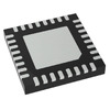
The EPM7256SQC208-10 is part of Intel's (formerly Altera) MAX® 7000S family, a high-performance CPLD range known for its robust programmability and logic optimization capabilities. This model boasts about 5,000 usable gates and includes 256 macrocells, housed within a 208-pin Plastic Quad Flat Pack (PQFP). It operates at a frequency up to 128.2 MHz and supports a 5.0 V operating voltage, with a maximum propagation delay of 7.5 ns and an operational temperature ceiling of +70°C. A key feature is its in-system programmability through a built-in IEEE Std. 1149.1 JTAG interface, enabling dynamic configuration. The MAX® 7000S devices are fabricated using advanced CMOS technology, offering features such as pin-to-pin logic delays as quick as 5 ns and counter frequencies reaching up to 175.4 MHz. The family presents a variety of package options and is designed with programmable macrocell flip-flops that contribute to substantial power savings over 50% reduction in some instances. Additionally, it includes a security bit for the protection of proprietary designs.
If your organization needs a solid programmable logic solution, the EPM7256SQC208-10 is a reliable choice, so contact us today to secure your bulk order.
EPM7256SQC208-10 CAD Models
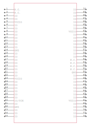
EPM7256SQC208-10 Symbol
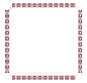
EPM7256SQC208-10 Footprint
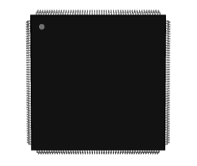
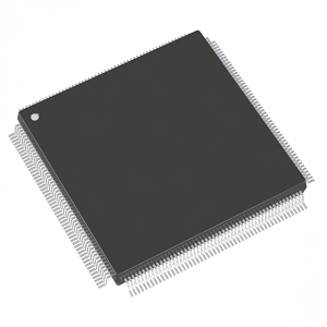
EPM7256SQC208-10 3D Model
EPM7256SQC208-10 Features
• High Logic Density: The EPM7256SQC208-10 provides about 5,000 usable gates and contains 256 macrocells. This high logic capacity makes it ideal for implementing complex combinational circuits and efficient logic integration in compact designs.
• Fast Performance: With a maximum operating frequency of 128.2 MHz and a propagation delay of just 7.5 ns, this CPLD ensures rapid processing and quick response times, good for high-speed applications.
• In-System Programmability (ISP): Equipped with an IEEE Std. 1149.1 JTAG interface, the device allows for in-system programming and testing without the need for physical removal, facilitating iterative development and updates.
• Advanced Architecture: Utilizing Altera's second-generation MAX architecture and fabricated with advanced CMOS technology, the EPM7256SQC208-10 offers enhanced performance and durability, ensuring reliability in various operational environments.
• Power Management: The device features programmable power-saving modes that can reduce power consumption by over 50% per macrocell, supporting energy-efficient designs and prolonging battery life in portable applications.
• Security Features: A programmable security bit provides protection against unauthorized access and copying of proprietary designs, safeguarding intellectual property effectively.
• Wide Operating Conditions: Operating at 5.0 V and capable of functioning in temperatures up to +70°C, this CPLD adapts to diverse environmental conditions, making it suitable for both industrial and commercial applications.
• Flexible I/O Standards: Supports MultiVolt™ I/O interface operations, compatible with both 3.3 V and 5.0 V systems. This flexibility allows seamless integration with existing and new hardware, reducing system complexity and costs.
• Design Support: The EPM7256SQC208-10 is supported by a range of design tools and programming hardware options, simplifying the development process and allowing to focus on innovation rather than compatibility issues.
EPM7256SQC208-10 Pinout Diagram
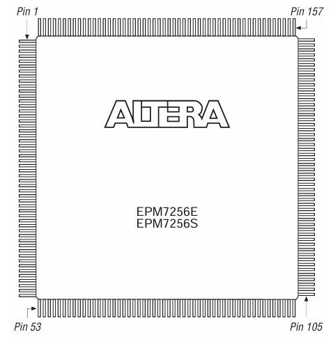
This diagram shows the pin layout for the EPM7256SQC208-10 chip from Altera. The chip has 208 pins, arranged on all four sides in a square shape. Pin 1 starts at the top-left corner and the numbers go around the chip in a counterclockwise direction, down the left side to Pin 53, across the bottom to Pin 105, up the right side to Pin 157, and back to the top-right. The labels help you know where to start and how to place the chip correctly on a circuit board. The name in the center, “EPM7256E / EPM7256S,” means this layout works for both chip versions. This diagram is important when connecting power, signals, or programming lines to the chip.
EPM7256SQC208-10 Block Diagram
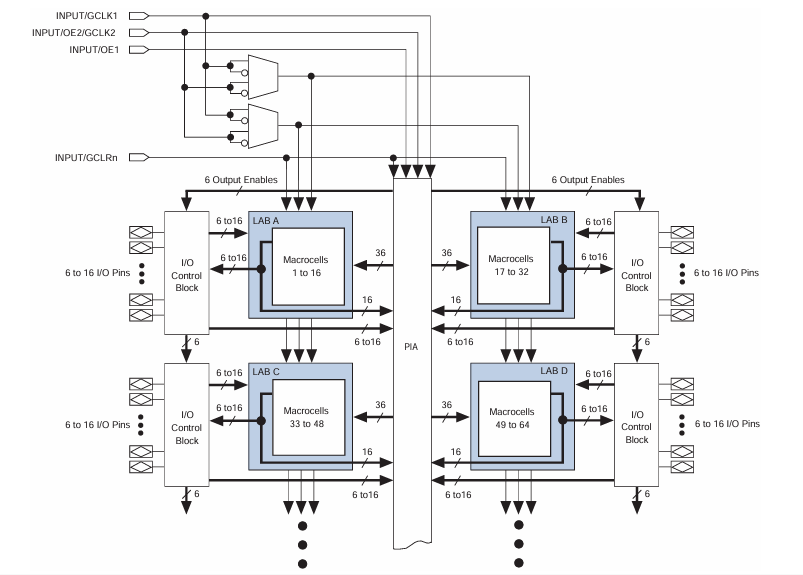
The block diagram of the EPM7256SQC208-10 shows how the chip is organized to handle digital logic tasks. It has four main logic blocks called LAB A, B, C, and D. Each block contains 16 macrocells, which are the basic building parts that do the logic work. So in total, there are 64 macrocells inside the chip. Around these logic blocks are I/O control blocks, which connect the chip to the outside world through input and output pins. Each control block manages 6 to 16 pins, letting signals go in or out of the chip as needed.
At the center is the Programmable Interconnect Array (PIA), which acts like a highway system, letting signals move between logic blocks and I/O pins. This allows you to route data any way you need for your design. At the top left, the diagram shows some control inputs like global clock (GCLK), output enable (OE), and clear (GCLR). These signals help manage the timing and behavior of the logic circuits across the chip.
EPM7256SQC208-10 Specifications
|
Type |
Parameter |
|
Manufacturer |
Altera/Intel |
|
Series |
MAX® 7000S |
|
Packaging |
Tray |
|
Part Status |
Obsolete |
|
Programmable Type |
In System Programmable |
|
Delay Time tpd(1) Max |
10 ns |
|
Voltage Supply - Internal |
4.75V ~ 5.25V |
|
Number of Logic Elements/Blocks |
16 |
|
Number of Macrocells |
256 |
|
Number of Gates |
5000 |
|
Number of I/O |
164 |
|
Operating Temperature |
0°C ~ 70°C (TA) |
|
Mounting Type |
Surface Mount |
|
Package / Case |
208-BFQFP |
|
Supplier Device Package |
208-PQFP (28x28) |
|
Base Product Number |
EPM7256 |
EPM7256SQC208-10 Applications
Industrial Automation
The EPM7256SQC208-10 is extensively used in industrial automation systems. Its high logic density and fast performance enable complex control tasks, interfacing seamlessly with sensors and actuators. This CPLD is ideal for enhancing precision and efficiency in production lines, process control systems, and robotic applications.
Telecommunications
In telecommunications, this CPLD excels in managing data flow and signal integrity across networks. It supports functions like signal conversion, routing, and processing in switches and routers, ensuring robust and efficient communication infrastructures.
Automotive Systems
In the automotive industry, this device contributes to the reliability and sophistication of systems such as engine management units, infotainment systems, and driver-assistance technologies. Its robust performance under varying conditions makes it suitable for safety-critical applications.
Medical Devices
The precision and programmability of the EPM7256SQC208-10 make it valuable in medical equipment, where accurate control and reliable operation are important. It is used in devices for monitoring patient vitals, managing diagnostic instruments, and automating treatment delivery.
Aerospace and Defense
In aerospace and defense, the EPM7256SQC208-10 is employed in systems requiring high levels of reliability and performance, such as satellite communications, navigation aids, and military hardware controls. Its ability to operate under extreme conditions is beneficial.
Educational and Research Institutions
This CPLD is also popular in educational settings and research projects, where its reprogrammability and flexibility facilitate experimentation and learning in digital design and electronics. It allows to prototype and test various logic designs efficiently.
EPM7256SQC208-10 Similar Parts
EPM7256SQC208-10 Programming Steps
1. Enter ISP Mode
This initial step is important as it transitions the CPLD from normal operation mode to In-System Programming (ISP) mode. This is achieved by sending a specific command through the JTAG interface. During this process, all I/O pins of the CPLD are tri-stated (disabled) to avoid any interference or conflicts with other circuit components. The transition into ISP mode prepares the device for safe programming and takes about 1 millisecond.
2. Check ID
Once in ISP mode, the system performs an ID check to ensure that the correct device is being programmed. This involves reading the device's unique silicon ID through the JTAG interface. This step is good for verifying that the programming commands and data will be sent to the correct device, preventing erroneous programming and potential device damage.
3. Bulk Erase
Before new data can be programmed, the existing data within the CPLD must be erased. The bulk erase step effectively clears all the programmable cells within the device. This is done by shifting in the erase instruction and then applying a 100-millisecond pulse which erases the entire chip. This step is important to ensure that no remnants of previous configurations interfere with the new programming.
4. Program
This step involves the actual programming of the CPLD where the new configuration data is written into the device. Data and corresponding addresses are shifted into the device through the JTAG interface. Each address and data pair requires a programming pulse to ensure the data is correctly written into the non-volatile memory cells of the CPLD. This step is repeated for each data point across the device's memory map.
5. Verify
Post-programming, it is need to verify that the data has been correctly written to the device. This verification step involves reading back the programmed data from each address and comparing it with the original input data. This step ensures data integrity and confirms that the programming process has been successful without any errors.
6. Exit ISP Mode
The final step in the programming process is to exit the ISP mode and return the CPLD to normal operational mode. This is done by sending another command via the JTAG interface. Upon successful exit, the I/O pins are reactivated, and the device resumes normal function. This step also typically takes about 1 millisecond.
EPM7256SQC208-10 Advantages
Non-Volatile Configuration
The EPM7256SQC208-10 utilizes EEPROM technology, allowing it to store its configuration permanently. This non-volatile nature means the device does not need to reload its configuration data from external memory every time it is powered on. This results in faster startup times and reduces the overall complexity of the hardware design by eliminating the need for additional configuration storage components.
In-System Programmability (ISP)
One of the standout features of the EPM7256SQC208-10 is its support for In-System Programmability. This allows the device to be programmed and reprogrammed while embedded in the end application without needing to be physically removed. This capability simplifies updates and modifications, providing flexibility and ease of use during development and throughout the lifecycle of the product.
High I/O Count and Logic Density
The device offers a substantial amount of logic resources and I/O pins, with 256 macrocells and 164 user I/O pins. This high I/O count and logic density enable the integration of multiple functions into a single chip, facilitating more complex designs while conserving space on the PCB. This advantage is beneficial in applications where board space is at a premium and multi-functionality is important.
Fast Pin-to-Pin Delay
With a maximum pin-to-pin delay of just 10 ns, the EPM7256SQC208-10 can perform high-speed logic operations. This quick response time is great in applications that require rapid processing capabilities, such as high-speed communications or computing, ensuring that the system meets stringent performance criteria.
Wide Voltage Compatibility
The EPM7256SQC208-10 is designed to be flexible in terms of voltage compatibility, supporting internal operation at 5 V and I/O levels at 3.3 V. This dual-voltage capability allows the device to interface easily with both 3.3 V and 5 V systems, reducing the need for voltage level translators and simplifying system design.
EPM7256SQC208-10 Packaging Dimensions
• Package Type: 208-BFQFP (Plastic Quad Flat Package)
• Number of Pins: 208 leads
• Body Size (L × W): 28 mm × 28 mm
• Mounting Style: Surface Mount Technology (SMT)
• Lead Pitch: Typically 0.5 mm between pins (standard for BFQFP)
• Package Material: Plastic
• Package Thickness: Approximately 3.5 mm (varies slightly by manufacturer)
• Thermal Characteristics: No exposed pad; standard ambient dissipation via board
• Tray Packaging: Supplied in trays for volume handling and pick-and-place automation
EPM7256SQC208-10 Manufacturer
The EPM7256SQC208-10 was originally developed and manufactured by Altera Corporation, a leading pioneer in programmable logic devices known for its MAX® 7000S series of CPLDs. In 2015, Altera was acquired by Intel Corporation, one of the world’s largest semiconductor manufacturers. Since the acquisition, Intel has continued to support and integrate Altera’s CPLD and FPGA technologies under its Programmable Solutions Group. The EPM7256SQC208-10 represents Intel’s legacy in offering high-performance, in-system programmable logic solutions tailored for a wide range of industrial, telecommunications, and embedded applications. Though now classified as obsolete, the part reflects Intel’s longstanding commitment to reliable and flexible programmable logic devices.
Conclusion
The EPM7256SQC208-10 is a smart and dependable chip that helps make digital systems run smoothly. It saves power, supports different voltages, and lets you program it while it’s already installed, which makes updates easy. Even though it’s now an older chip, others still use it because it works well in all kinds of systems. If you need a solid chip for controlling logic in your design, this one is a great option. Contact us today if you want to order it in bulk.
Datasheet PDF
EPM7256SQC208-10 Datasheets:
Cylindrical Battery Holders.pdf
About us
ALLELCO LIMITED
Read more
Quick inquiry
Please send an inquiry, we will respond immediately.
Frequently Asked Questions [FAQ]
1. What programming tools are compatible with the EPM7256SQC208-10?
You can use Intel’s Quartus II software (formerly Altera Quartus), along with a JTAG-compatible programmer like the USB-Blaster, to configure and program the EPM7256SQC208-10 directly in-system.
2. Can I reprogram the EPM7256SQC208-10 multiple times?
Yes, the EPM7256SQC208-10 supports multiple reprogramming cycles using its EEPROM-based in-system programmability, making it ideal for iterative design development or post-deployment updates.
3. Can the EPM7256SQC208-10 handle harsh operating conditions?
It operates reliably within a commercial temperature range of 0°C to +70°C, which is sufficient for most industrial and embedded applications, though not for extreme or automotive-grade environments.
4. Can I still program the EPM7256SQC208-10 without removing it from the circuit board?
Yes. The chip supports In-System Programmability (ISP) via JTAG, allowing you to reprogram it while it's already soldered onto your board, saving time and effort during development or maintenance.
5. What makes the EPM7256SQC208-10 better than a standard microcontroller for logic tasks?
Unlike microcontrollers, the EPM7256SQC208-10 is a CPLD, which excels at executing parallel logic operations with precise timing. It’s ideal when you need fast, deterministic digital control over multiple signals.

DeMorgan’s Theorems Explained: Simplifying Logic Expressions for Better Circuit Design
on April 25th
Norton Theorem Basics and Circuit Examples
on April 24th
Popular Posts
-

Complex Instruction Set Computers: How They Changed Computing?
on April 18th 147765
-

USB-C Pinout and Features
on April 18th 111994
-

Using Xilinx Unified Simulation Primitives: A Comprehensive Guide to FPGA Design and Simulation
on April 18th 111351
-

Power Supply Voltages in Electronics: Meaning of VCC, VDD, VEE, VSS, and GND
on April 18th 83753
-

RJ45 Connector Guide: Pinout, Wiring, Cable Types, and Uses
on January 1th 79548
-

The Ultimate Guide to Wire Color Codes in Modern Electrical Systems
The way our electrical systems use colors isn’t just for looks. Each wire color now indicates a specific function, making it easier to identify and handle electrical components correctly during ins...on January 1th 66949
-

Purge Valve Guide: Function, Symptoms, Testing, and Replacement for Optimal Engine Performance
The purge valve is a key part of a car’s system that helps keep the air clean by managing fuel vapors before they can escape into the atmosphere. This not only helps the environment by reducing pol...on January 1th 63094
-

Quality (Q) Factor: Equations and Applications
The quality factor, or 'Q', is important when checking how well inductors and resonators work in electronic systems that use radio frequencies (RF). 'Q' measures how well a circuit minimizes energy...on January 1th 63028
-

Achieving Peak Performance with the Maximum Power Transfer Theorem
The Maximum Power Transfer Theorem explains how energy from a source, such as a battery or generator, flows to a connected load. It shows the exact condition where the load receives the most power....on January 1th 54094
-

A23 Battery Specifications and Compatibility
The A23 battery is a small, cylinder-shaped battery with high voltage. Also called 23A, 23AE, or MN21, it runs at 12 volts and much higher than AA or AAA batteries. Its special design make...on January 1th 52175
HOT Part Number
-

SP6205EM5-L/TR
MaxLinear, Inc.
IC REG LIN POS ADJ 500MA SOT23-5
MAX6163AESA+T
Analog Devices Inc./Maxim Integrated
IC VREF SERIES 0.07% 8SOIC
BM06B-XASS-TF
JST Sales America Inc.
CONN HEADER SMD 6POS 2.5MM
ADS7861E
Texas Instruments
IC ADC 12BIT SAR 24SSOP
AD8605ACB-REEL7
Analog Devices Inc.
IC OPAMP GP R-R CMOS PREC 5WLCSP
GRM2165C2A121JA01D
Murata Electronics
CAP CER 120PF 100V C0G/NP0 0805
AD7576JN
Analog Devices Inc.
8-BIT SAR ADC, PARALLEL ACCESS
1N5386BG
onsemi
DIODE ZENER 180V 5W AXIAL
FAN1655M
onsemi
IC REG CTRLR DDR 1OUT 14SOIC
JW100H1
ABB Power Electronics Inc.
DC DC CONVERTER 24V 100W
EMH2412-TL-H
Sanyo
N-CHANNEL MOSFET
PIC16F818T-I/SO
Microchip Technology
IC MCU 8BIT 1.75KB FLASH 18SOIC
CD4030BPWR
Texas Instruments
IC GATE XOR 4CH 2-INP 14TSSOP
AD7175-8BCPZ-RL
Analog Devices Inc.
IC ADC 24BIT SIGMA-DELTA 40LFCSP
TH72032KDC-BAA-000-RE
Melexis Technologies NV
RF XMITTER ASK 868/915MHZ 8SOIC
T520V227M006ATE040
KEMET
CAP TANT POLY 220UF 6.3V 2917
NVD14N03RT4G
onsemi
N-CHANNEL POWER MOSFET
RT0805DRD0751KL
YAGEO
RES SMD 51K OHM 0.5% 1/8W 0805 -
LTC2229IUH#PBF
Analog Devices Inc.
IC ADC 12BIT PIPELINED 32QFN
BC856A
Taiwan Semiconductor Corporation
SOT-23, -80V, -0.1A, PNP BIPOLAR
74ACT574
AMI Semiconductor / ON Semiconductor
IC FF D-TYPE SNGL 8BIT DIE
A4949GLJTR-T
Allegro MicroSystems
IC FAN DRIVER BLDC 8SOIC
SD417+
Analog Devices Inc./Maxim Integrated
MODULE INTERFACE SENSOR
BQ24032RHLR
Texas Instruments
IC BATT CHG LI-ION 1CELL 20VQFN
SMBJ8.5A
Meritek
TVS DIODE 8.5VWM 14.4VC
W25Q256JVFJM
Winbond Electronics
IC FLASH 256MBIT SPI/QUAD 16SOIC
IPP086N10N3
Infineon Technologies
N-CHANNEL POWER MOSFET
TNY266PN
Power Integrations
IC OFFLINE SWITCH FLYBACK 8DIP
X9511WS
Intersil
DIGIPOT, 32 POSITIONS
GRM1555C1E7R4CZ01D
Murata Electronics
CAP CER 7.4PF 25V C0G/NP0 0402
XC6218P302HR-G
Torex Semiconductor Ltd
IC REG LINEAR 3V 200MA 3USP
HI5812JIP
Renesas Electronics America Inc
IC ADC 12BIT SAR 24DIP
MCIMX503CVM8B
NXP USA Inc.
IC MPU I.MX50 800MHZ 400MAPBGA
281742-5
TE Connectivity AMP Connectors
CONN HEADER R/A 10POS 2.54MM
RT1206DRD0724KL
YAGEO
RES SMD 24K OHM 0.5% 1/4W 1206
KSZ8041NL-TR
Microchip Technology
IC TRANSCEIVER FULL 1/1 32MLF -
MAX802MCSA+
Analog Devices Inc./Maxim Integrated
IC SUPERVISOR 1 CHANNEL 8SOIC
MCP1811AT-033/OT
Microchip Technology
IC REG LINEAR 3.3V 150MA SOT23-5
MIC5355-SGYMME
Microchip Technology
IC REG LINEAR 1.8V/3.3V 8MSOP
08051A151GA12A
KYOCERA AVX
CAP CER 150PF 100V NP0 0805
MC33772BSP1AE
NXP USA Inc.
IC BATT CNTRL LI-ION 3-6C 48LQFP
MAX3964AETP
Analog Devices Inc./Maxim Integrated
IC LIMITING AMP 20TQFN
KSP43TA
onsemi
TRANS NPN 200V 0.5A TO92-3
ADM3485EAN
Analog Devices Inc.
IC TXRX RS-485 HS 3.3V 8DIP
GRM0225C1C6R8DD05L
Murata Electronics
CAP CER 6.8PF 16V C0G/NP0 01005
C1608Y5V1C105Z/10
TDK Corporation
CAP CER 1UF 16V Y5V 0603
P6KE110CA
SMC Diode Solutions
TVS DIODE 94VWM 152VC DO15
AR2003FV-13
Diodes Incorporated
IC RECT CTRLR ACT/SYNC 14VDFN
744761156C
Würth Elektronik
FIXED IND 56NH 600MA 250MOHM SMD
MT29F4G08ABADAH4-IT:D
Micron Technology Inc.
IC FLASH 4GBIT PARALLEL 63VFBGA
MP2012DQ-LF-Z
Monolithic Power Systems Inc.
IC REG BUCK ADJUSTABLE 1.5A 6QFN
SN74AHC04NSR
Texas Instruments
IC INVERTER 6CH 1-INP 14SOP
PIC16C54C-20I/SS
Microchip Technology
IC MCU 8BIT 768B OTP 20SSOP
MJE371
onsemi
TRANS PNP 40V 4A TO126