Erasable Programmable Logic Devices (EPLDs): A Guide to Design and Applications
This guide introduces Erasable Programmable Logic Devices (EPLDs), a flexible and reusable technology in integrated circuits. Unlike traditional programmable devices, EPLDs can be reconfigured multiple times, making them ideal for evolving design needs. We’ll explore their capabilities, applications in industries like telecommunications and automotive, and key factors to consider when using these versatile devices in modern electronics.Catalog
Overview
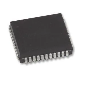
Erasable Programmable Logic Devices (EPLDs), introduced in the mid-1980s by Aitera, revolutionized programmable logic with their high integration density and flexibility, surpassing the capabilities of similar devices like Generic Array Logic (GAL). EPLDs enable a broader range of logic functions within a single chip, making them versatile and efficient for various applications. Their reprogrammability allows to adapt designs without replacing hardware, a key advantage in industries like telecommunications and automotive, where rapid prototyping is needed. EPLDs' compact design and low power consumption make them ideal for embedded systems and portable devices, highlighting their technical and practical advantages in modern digital logic design.
PLD Device Design Steps
Designing a Programmable Logic Device (PLD) involves several steps to create a functional and efficient design.
The process begins with defining the circuit logic functions. This can be done using either schematic diagrams or Hardware Description Languages (HDLs). Schematic diagrams provide a straightforward way to visualize basic logic circuits but are less effective for handling complex designs. In contrast, HDLs offer a more concise and flexible way to describe logic functions, making them the preferred choice for modern PLD designs.
Next, designers choose a suitable HDL for their project. Popular options include ABEL, VHDL, and Verilog. ABEL is ideal for simpler designs, like counters or encoders, because it uses Boolean equations and truth tables. VHDL is more structured and excels in handling complex logic, making it suitable for intricate projects. Verilog, with its compact, C-like syntax, is great for both logic design and simulation, making it a versatile option for advanced applications. The choice of HDL depends on the project's complexity and specific requirements.
Once the logic functions are defined, the next step is programming and simulation. Specialized software compiles the described logic and converts it into Boolean expressions, which are then saved as a JEDEC (JED) file. Before the design is transferred to hardware, simulations are performed within the software to verify that the logic functions as intended. This simulation phase is important, as it ensures the design meets performance specifications and reduces the likelihood of errors during implementation.
Finally, the design is downloaded to the PLD device. This involves transferring the JEDEC file to the hardware using a programmer, a device specifically designed to write the file into PLDs such as PROMs, EEPROMs, GALs, CPLDs, or PALs. Programmers connect to a computer via a parallel port and accurately load the design onto the hardware. This step completes the process, transforming the design from a digital model into a physical, functioning device.
The PLD design process involves four main steps: defining the logic functions, choosing an appropriate HDL, programming and simulating the design, and downloading the final design to the hardware. Each stage plays a role in ensuring the success and reliability of the device. As tools and methods continue to evolve, PLD designs are becoming more flexible, efficient, and capable of handling increasingly complex applications.
About us
ALLELCO LIMITED
Read more
Quick inquiry
Please send an inquiry, we will respond immediately.

Complex Instruction Set Computers: How They Changed Computing?
on December 30th
Exploring the Versatility of MP (Microprocessor) Technology
on December 30th
Popular Posts
-
Complex Instruction Set Computers: How They Changed Computing?
on April 18th 147749
-

USB-C Pinout and Features
on April 18th 111893
-

Using Xilinx Unified Simulation Primitives: A Comprehensive Guide to FPGA Design and Simulation
on April 18th 111349
-

Power Supply Voltages in Electronics: Meaning of VCC, VDD, VEE, VSS, and GND
on April 18th 83713
-

RJ45 Connector Guide: Pinout, Wiring, Cable Types, and Uses
on January 1th 79502
-

The Ultimate Guide to Wire Color Codes in Modern Electrical Systems
The way our electrical systems use colors isn’t just for looks. Each wire color now indicates a specific function, making it easier to identify and handle electrical components correctly during ins...on January 1th 66865
-

Quality (Q) Factor: Equations and Applications
The quality factor, or 'Q', is important when checking how well inductors and resonators work in electronic systems that use radio frequencies (RF). 'Q' measures how well a circuit minimizes energy...on January 1th 63001
-

Purge Valve Guide: Function, Symptoms, Testing, and Replacement for Optimal Engine Performance
The purge valve is a key part of a car’s system that helps keep the air clean by managing fuel vapors before they can escape into the atmosphere. This not only helps the environment by reducing pol...on January 1th 62925
-

Achieving Peak Performance with the Maximum Power Transfer Theorem
The Maximum Power Transfer Theorem explains how energy from a source, such as a battery or generator, flows to a connected load. It shows the exact condition where the load receives the most power....on January 1th 54071
-

A23 Battery Specifications and Compatibility
The A23 battery is a small, cylinder-shaped battery with high voltage. Also called 23A, 23AE, or MN21, it runs at 12 volts and much higher than AA or AAA batteries. Its special design make...on January 1th 52087
HOT Part Number
-
NCV7720DQAR2G
onsemi
IC MOTOR DRIVER 24SSOP
1N5227B
SMC Diode Solutions
DIODE ZENER 3.6V 500MW DO35
ADS7830IPWR
Texas Instruments
IC ADC 8BIT SAR 16TSSOP
NP60N06PDK-E1-AY
Renesas Electronics America Inc
MOSFET TRANSISTOR MORE 1 W
TL441CN
Texas Instruments
IC LOGARITHMIC 1 CIRCUIT 16DIP
2SAR514P5T100
Rohm Semiconductor
TRANS PNP 80V 0.7A MPT3
SMA6J18A-TR
STMicroelectronics
TVS DIODE 18VWM 33.2VC SMA
C8051F124
Silicon Labs
IC MCU 8BIT 128KB FLASH 100TQFP
2N5089
NTE Electronics, Inc
TRANS NPN 25V 0.05A TO92
18121C104JAT2A
KYOCERA AVX
CAP CER 0.1UF 100V X7R 1812
HCPL-7721-060E
Broadcom Limited
OPTOISO 3.75KV PUSH PULL 8DIP
NCT72CMTR2G
onsemi
SENSOR DIGITAL -40C-125C 8WDFN
AMK316AC7476MLHT
Taiyo Yuden
CAP CER 47UF 4V X7S 1206
AT17C65-10JC
Microchip Technology
IC SERIAL CONFIG PROM 64K 20PLCC
AD5248BRMZ100-RL7
Analog Devices Inc.
IC DGT POT 100KOHM 256TAP 10MSOP
PIC32MZ2048EFM100-E/GJX
Microchip Technology
IC MCU 32BIT 2MB FLASH 100TFBGA
12101K3R9CBTTR
KYOCERA AVX
CAP THIN FILM 3.9PF 100V 1210
GBPC5010W
GeneSiC Semiconductor
BRIDGE RECT 1P 1KV 50A GBPC-W -

UMK316F474ZF-T
Taiyo Yuden
CAP CER 0.47UF 50V Y5V 1206
CY25100SXC-064T
Infineon Technologies
IC CLOCK GENERATOR
9UMS9633BKLF
Renesas Electronics America Inc
IC MOBILE PC CLK EMEBED 48VFQFPN
AFT05MP075NR1
NXP USA Inc.
FET RF 2CH 40V 520MHZ TO270-4
LFE3-150EA-7FN672I
Lattice Semiconductor Corporation
IC FPGA 380 I/O 672FPBGA
VC060309A200RP
KYOCERA AVX
VARISTOR 12.7V 30A 0603
IRS44262STRPBF
Infineon Technologies
IC GATE DRVR LOW-SIDE 8SOIC
CY2544C016
Infineon Technologies
TSBU
MIC2551AYML
Micrel Inc.
USB TRANSCEIVER
DRV5021A3EDBZRQ1
Texas Instruments
MAGNETIC SWITCH UNIPOLAR SOT23-3
SY88343BLEY
Microchip Technology
IC LIMITING 1 CIRCUIT 10MSOP
AOT440
Alpha & Omega Semiconductor Inc.
MOSFET N-CH 40V 15.5A/105A TO220
VI-2W2-EW
Vicor Corporation
DC DC CONVERTER 15V 100W
MCP6292IDR
Texas Instruments
IC OPAMP GP 2 CIRCUIT 8SOIC
ATF750C-15JI
Microchip Technology
IC CPLD 10MC 15NS 28PLCC
640550-7
TE Connectivity AMP Connectors
CONN DUST COVER 7POS CLOSED
PM10CZF120
Powerex Inc.
MOD IPM 6PAC 1200V 10A
TLC277CP
Texas Instruments
IC CMOS 2 CIRCUIT 8DIP -

RT1206BRD071K2L
YAGEO
RES SMD 1.2K OHM 0.1% 1/4W 1206
SN74F163ANS
Texas Instruments
IC BINARY COUNTER 4-BIT 16SO
ATA664251-WGQW
Microchip Technology
IC MCU 8BIT 16KB FLASH 48QFN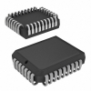
AT28BV64-30JC
Microchip Technology
IC EEPROM 64KBIT PARALLEL 32PLCC
GBPC2508
Yangjie Technology
GBPC 800V 25.0A Diodes Bridge
MT47H128M16RT-25E IT:C
Micron Technology Inc.
IC DRAM 2GBIT PARALLEL 84FBGA
AD9644BCPZ-80
Analog Devices Inc.
IC ADC 14BIT PIPELINED 48LFCSP
MK21DX256VLK5
NXP USA Inc.
IC MCU 32BIT 256KB FLASH 80FQFP
FQPF3N90
Fairchild Semiconductor
MOSFET N-CH 900V 2.1A TO220F
74HC541D,653
NXP USA Inc.
IC BUFF/DVR TRI-ST 8BIT 20SOIC
MX25V8035ZNI-15G
Macronix
IC FLASH 8MBIT SPI 66MHZ 8WSON
P6SMB18CA
Taiwan Semiconductor Corporation
TVS DIODE 15.3VWM 25.5VC DO214AA
AUIPS7091S
Infineon Technologies
IC PWR SWITCH N-CHAN 1:1 D2PAK-5
RP122K331D-TR
Nisshinbo Micro Devices Inc.
IC REG LIN 3.3V 400MA DFN1010-4
GALI-51+
Mini-Circuits
IC AMP CELLULAR 0HZ-4GHZ SOT89
770901-1
TE Connectivity AMP Connectors
CONN PIN 22-26AWG TIN CRIMP
IPA60R800CEXKSA1
Infineon Technologies
MOSFET N-CH 600V 5.6A TO220-FP
P4SMA91A
Meritek
TVS DIODE 77.8VWM 125VC