Exploring the 74HC02: Pinout, and Application Circuits
The 74HC02 Quad 2-Input NOR Gate is a key component in digital electronics, valued for its speed, low power consumption, and compatibility with various logic families. Ideal for simplifying complex logic designs, it finds use in fields like signal processing and automation. This article explores the 74HC02’s datasheet, features, and applications, highlighting its role in memory systems, secure digital architectures, and control signal optimization. Discover how this versatile IC continues to innovate and enhance digital circuit design.Catalog

74HC02 Overview
The 74HC02 is an integrated circuit that features four distinct 2-input NOR gates. Each gate is equipped with input clamp diodes, which work hand in hand with current-limiting resistors to manage instances when input values exceed the VCC. In the landscape of digital circuitry, the NOR gate stands as an initial logic element. Its simplicity shines through its operation: it outputs a high signal solely when both inputs are low. Therefore, the 74HC02 becomes a required part of crafting various logical functions.
In practical terms, the 74HC02 can often streamline circuit designs by reducing the component count needed for complex logic tasks. The NOR gate shines when two or more conditions exclusively must be met to generate an output. Consumer electronics serve as an illustrative example. You can frequently turn to this IC to navigate controls that should only trigger under specific conditions—like the automatic standby modes seen in televisions.
The adaptability of the 74HC02 branches out from elementary applications, finding its place in intricate systems. It serves as a key element in building flip-flops and latches. These components are used in timing circuits present in memory chips and processors. Moreover, the 74HC02 proves to be a subtle catalyst for innovation in troubleshooting and repair, where grasping the logic flows paves the way for more effective diagnostics.
Features and Technical Specifications
Features
|
Feature |
Description |
|
Operating Voltage Range |
Wide range of 2.0 V to 6.0 V |
|
Power Dissipation |
Low power consumption with CMOS technology |
|
Noise Immunity |
High noise immunity |
|
Latch-Up Performance |
Robust latch-up performance exceeding 100 mA (JESD 78
Class II Level B) |
|
Input Levels |
- 74HC02: CMOS level |
|
- 74HCT02: TTL level |
|
|
Compliance with JEDEC Standards |
- JESD8C: 2.7 V to 3.6 V |
|
- JESD7A: 2.0 V to 6.0 V |
|
|
ESD Protection |
- HBM JESD22-A114F: Exceeds 2000 V |
|
- MM JESD22-A115-A: Exceeds 200 V |
|
|
Package Options |
Various package options available |
|
Temperature Range Specifications |
Provided for -40 °C to +85 °C and -40 °C to +125 °C |
Specifications
|
Type |
Parameter |
|
Max Power Dissipation |
500mW |
|
Propagation Delay |
15 ns |
|
Quiescent Current |
2μA |
|
Turn On Delay Time |
7 ns |
|
Logic Level - Low |
0.5V ~ 1.8V |
|
Logic Level - High |
1.5V ~ 4.2V |
|
Current - Output High, Low |
5.2mA, 5.2mA |
|
Output Current |
25mA |
|
Number of Functions |
4 |
Applications of 74HC02
The 74HC02 houses four separate NOR gates, each attuned for sophisticated logical operations. These gates uniquely emit a HIGH signal only when every input registers as LOW, as illustrated by its truth table. This characteristic empowers NOR gates to be initial elements in digital circuit creation, underpinning complex logic functionalities. By strategically configuring them, these gates adeptly emulate other logic gates such as AND, OR, and NOT.

Digital Systems
In the world of digital systems, NOR gates exemplified by the 74HC02 offer expansive opportunities for developing adaptable and robust logic circuits. They enable you to integrate basic functions and control elements in computational devices. Through efficient combinations, these gates execute negation and conjunction, which are core facets of computational processes. You can frequently depend on their capacity to streamline circuit architecture, enhancing overall operational efficacy and system dependability.
•Memory and Storage: Widespread application of NOR gates can be observed in memory and storage technologies. As basic components in constructing memory cells, they facilitate data management processes in both volatile and non-volatile memories. Their role is mostly noteworthy in flash memory innovations, where their incorporation supports high-capacity data storage with reduced power requirements. Such advancements emphasize NOR gates' remarkable contribution to evolving everyday electronic memory technologies.
Security Systems
NOR gates in the 74HC02 significantly bolster the security capabilities of digital configurations. Masterful application of these gates enables the execution of intricate security protocols. Logical configurations, such as those employed in encryption algorithms, leverage these gates to shield sensitive data from unauthorized exposure. Consequently, the strength of NOR gates is key in forming secure system architectures that are useful for maintaining data integrity and protecting your confidentiality.
Control Signal Management
In addition, the 74HC02 exerts influence over control signal management in numerous electronic systems. NOR gates are instrumental in directing signal pathways, facilitating accurate control over timing, and the sequential execution of tasks in microcontrollers and processors. This level of control is active for maximizing system performance and ensuring synchrony among diverse components within a digital framework.
Implementation of the 74HC02 Chip
The 74HC02 integrated circuit holds notable significance within the expansive 7400 series, inviting thoughtful reflection on its functional specifications and conceivable uses. It plays a role in systems that parlay creativity and problem-solving desires into innovative circuit designs.

Power Supply and Setup
The circuit demands steadiness in its power source, operational within a VCC spectrum of 2V to 6V. Such adaptability presents opportunities for its integration across a myriad of systems, supporting a full range of power demands. Securing the power pins with confidence ensures operational stability and avoids unwanted disruptions.
Basic NOR Gate Operation
Comprised of four separate NOR gates, the 74HC02 chip requires minimal input, serving as an ultimate component for developing more intricate logic circuits. You can frequently employ these gates in digital logic design.
Electrical Performance and Strategic Planning
Output current limits, peaking at 4 mA per gate when operating at 5V, frame the application's boundaries. This factor encourages meticulous load assessments to prevent overstraining outputs, achieving a harmony of reliability. You might infuse buffer gates within circuits, skillfully managing currents to protect and prolong the IC's viability.
Creative Applications of NOR Gates in Circuitry
NOR gates serve as typical elements in the world of digital electronics. By configuring them aptly, one can create any Boolean function, underlining their exceptional flexibility. You can dig into versatile applications for these gates, such as constructing latches and oscillators, showcasing the chip's adaptation potential to fulfill the intricate needs of unique and creative designs.
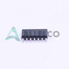
Pin Configuration
The 74HC02 integrated circuit features a total of 14 pins and includes four basic NOR gates, meticulously organized as depicted in the accompanying pinout diagram for optimal clarity and functionality.

|
Pin No. |
Pin Name |
Type |
Description |
|
1 |
1Y |
Output |
Output from the first NOR gate. |
|
2 |
1A |
Input |
Input to the first NOR gate. |
|
3 |
1B |
Input |
Input to the first NOR gate. |
|
4 |
2Y |
Output |
Output from the second NOR gate. |
|
5 |
2A |
Input |
Input to the second NOR gate. |
|
6 |
2B |
Input |
Input to the second NOR gate. |
|
7 |
GND |
Power |
Connect to ground. |
|
8 |
3A |
Input |
Input to the third NOR gate. |
|
9 |
3B |
Input |
Input to the third NOR gate. |
|
10 |
3Y |
Output |
Output from the third NOR gate. |
|
11 |
4A |
Input |
Input to the fourth NOR gate. |
|
12 |
4B |
Input |
Input to the fourth NOR gate. |
|
13 |
4Y |
Output |
Output from the fourth NOR gate. |
|
14 |
Vcc |
Power |
Positive power supply. Connect to +5V power. |
CAD Model
Symbol

Footprint

3D Model

Circuit Integration with 74HC02
Functional Diagram

Test Circuit

Using the 74HC02 IC to Build an SR Latch Circuit
The 74HC02 IC is a versatile component commonly used in simple yet important electronics projects. One practical example is constructing an SR (Set-Reset) latch, a circuit that allows you to control an LED using the IC's NOR gates. This design demonstrates the "memory" function of an SR latch—where the LED stays lit even after the initial button press is released.

Required Components
To build this circuit, gather the following:
• 1 x 74HC02 IC: The main component, providing the NOR gates.
• 1 x LED (L1): Displays the output state (on or off).
• 2 x 10 kΩ resistors (R1, R2): Regulate the voltage levels for stable operation of the circuit.
• 1 x 1 kΩ resistor (R3): Protects the LED by limiting the current passing through it.
• 2 x pushbuttons (S1, S2): Allow you to toggle the LED’s state (turn it on or off).
Alternatives and Comparable ICs for 74HC02
The 74HC02 IC offers a range of variations, each maintaining its core features while exhibiting differences in voltage and current handling abilities. Several noteworthy options include:
• 74HCT02
• 74LS02
• 74LVC02
• 74AC02
• 74ALS02
• 74F02
• 74C02
Maximum Ratings of 74HC02
|
Symbol |
Parameter |
Value |
Unit |
|
Vcc |
DC Supply Voltage (Referenced to GND) |
– 0.5 to +7.0 |
V |
|
Vin |
DC Input Voltage (Referenced to GND) |
– 0.5 to VCC + 0.5 |
V |
|
Vout |
DC Output Voltage (Referenced to GND) |
– 0.5 to VCC + 0.5 |
V |
|
lin |
DC Input Current, per Pin |
±20 |
mA |
|
Iout |
DC Output Current, per Pin |
±25 |
mA |
|
Icc |
DC Supply Current, VCC and GND Pins |
±50 |
mA |
|
PD |
Power Dissipation in Still Air: |
||
|
- SOIC Package |
500 |
mW |
|
|
- TSSOP Package |
450 |
mW |
|
|
Tstg |
Storage Temperature |
– 65 to +150 |
℃ |
|
TL |
Lead Temperature, 1 mm from Case for 10 Seconds: |
||
|
- SOIC or TSSOP Package |
260 |
℃ |
Operational Contexts
|
Symbol |
Parameter |
Min |
Max |
Unit |
|
Vcc |
DC Supply Voltage (Referenced to GND) |
2 |
6 |
V |
|
Vin, Vout |
DC Input Voltage, Output Voltage (Referenced to GND) |
0 |
Vcc |
V |
|
TA |
Operating Temperature, All Package Types |
-55 |
125 |
℃ |
|
tr, tf |
Input Rise and Fall Time (74HC02 waveforms figure) |
ns |
||
|
- Vcc = 2.0 V |
0 |
1000 |
||
|
- Vcc = 4.5 V |
0 |
500 |
||
|
- Vcc = 6.0 V |
0 |
400 |

About us
ALLELCO LIMITED
Read more
Quick inquiry
Please send an inquiry, we will respond immediately.
Frequently Asked Questions [FAQ]
1. What is the function of a NOR gate?
A NOR gate combines the functions of an OR gate and an inverter. It produces a true output only when both inputs are false. This characteristic is active for simplifying digital logic circuits, as it provides both negation and conjunction operations. Using NOR gates enhances both the reliability and efficiency of various applications by reducing circuit complexity.
2. What voltage range does the 74HC02 operate within?
The 74HC02 IC operates within a voltage range of 2.7 V to 3.6 V. This range is mostly beneficial in digital electronics, enabling easy integration with various digital systems while maintaining low power consumption. This attribute is especially important in battery-powered devices and allows for the integration of different logic families in mixed-voltage environments.
3. What are the benefits of using NOR gates?
NOR gates are compact and cost-effective, making them an excellent choice for reducing material costs. Their simple design facilitates rapid development and prototyping, allowing you to focus on improving other aspects of their systems. Incorporating NOR gates in circuit designs can simplify the system, potentially enhancing durability and performance.
4. How do NOR gates compare to NAND gates?
Choosing between NOR and NAND gates depends on specific needs such as speed, power consumption, cost, and circuit design complexity. NOR gates are often preferred in applications requiring fast performance and low power usage. On the other hand, NAND gates are simpler, which can lead to cost savings and ease of design in large-scale integration (VLSI) circuits. The decision should be based on a careful evaluation of these factors relative to the application's requirements.
The New Allegro ACS773 Current Sensor with Galvanic Isolation
on November 28th
LM2904 Dual Op-Amps: Features, Pinout, and Applications
on November 28th
Popular Posts
-

Complex Instruction Set Computers: How They Changed Computing?
on April 18th 147749
-

USB-C Pinout and Features
on April 18th 111904
-

Using Xilinx Unified Simulation Primitives: A Comprehensive Guide to FPGA Design and Simulation
on April 18th 111349
-

Power Supply Voltages in Electronics: Meaning of VCC, VDD, VEE, VSS, and GND
on April 18th 83714
-

RJ45 Connector Guide: Pinout, Wiring, Cable Types, and Uses
on January 1th 79502
-

The Ultimate Guide to Wire Color Codes in Modern Electrical Systems
The way our electrical systems use colors isn’t just for looks. Each wire color now indicates a specific function, making it easier to identify and handle electrical components correctly during ins...on January 1th 66869
-

Quality (Q) Factor: Equations and Applications
The quality factor, or 'Q', is important when checking how well inductors and resonators work in electronic systems that use radio frequencies (RF). 'Q' measures how well a circuit minimizes energy...on January 1th 63004
-

Purge Valve Guide: Function, Symptoms, Testing, and Replacement for Optimal Engine Performance
The purge valve is a key part of a car’s system that helps keep the air clean by managing fuel vapors before they can escape into the atmosphere. This not only helps the environment by reducing pol...on January 1th 62942
-

Achieving Peak Performance with the Maximum Power Transfer Theorem
The Maximum Power Transfer Theorem explains how energy from a source, such as a battery or generator, flows to a connected load. It shows the exact condition where the load receives the most power....on January 1th 54076
-

A23 Battery Specifications and Compatibility
The A23 battery is a small, cylinder-shaped battery with high voltage. Also called 23A, 23AE, or MN21, it runs at 12 volts and much higher than AA or AAA batteries. Its special design make...on January 1th 52087
HOT Part Number
-
LTC4063EDD#TRPBF
Analog Devices Inc.
IC BATT CHG LI-ION 1CELL 10DFN
MIMX8MM1CVTKZAA
NXP USA Inc.
IC MPU I.MX 8M MINI SOLOLITE
APDS-9005-020
Broadcom Limited
SENSOR OPT 500NM AMB 6CHIPLED
06031A820KAT2A
KYOCERA AVX
CAP CER 82PF 100V C0G/NP0 0603
ICM-20602
TDK InvenSense
IMU ACCEL/GYRO/TEMP I2C/SPI LGA
170M4611
Eaton - Bussmann Electrical Division
FUSE SQUARE 350A 700VAC RECT
08053C105JAZ2A
KYOCERA AVX
CAP CER 1UF 25V X7R 0805
EP1C12F324C6N
Intel
IC FPGA 249 I/O 324FBGA
2SC4617T1G
onsemi
TRANS NPN 50V 0.1A SC75 SOT416
TL431AILPRAG
onsemi
IC VREF SHUNT ADJ 1% TO92-3
ADAU1787BCBZRL
Analog Devices Inc.
4 ADC, 2 DAC LOW POWER CODEC, AU
74VHC164MTCX
onsemi
IC SHIFT REGISTER 8BIT 14TSSOP
DAN222M3T5G
onsemi
DIODE ARRAY GP 80V 100MA SOT723
NR3015T470M
Taiyo Yuden
FIXED IND 47UH 300MA 1.608OHM SM
MM3Z18VC
onsemi
DIODE ZENER 18V 200MW SOD323F
1N4001W
Rectron USA
DIODE GEN 1A 50V SOD-123F
SMBJ90A
Taiwan Semiconductor Corporation
TVS DIODE 90VWM 146VC DO214AA
NTA1215MC
Murata Power Solutions Inc.
DC DC CONVERTER +/-15V 1W -
SDR1307-101KL
Bourns Inc.
FIXED IND 100UH 1.9A 180MOHM SMD
AOT5B65M1
Alpha & Omega Semiconductor Inc.
IGBT 650V 5A TO220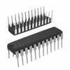
STP16CP596B1R
STMicroelectronics
IC LED DRIVER LINEAR 50MA 24DIP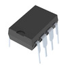
AD7895ANZ-2
Analog Devices Inc.
IC ADC 12BIT SAR 8DIP
MURB1620CTT4G
onsemi
DIODE ARRAY GP 200V 8A D2PAK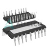
STGIPS30C60T-H
STMicroelectronics
MOD IPM SLLIMM 30A 600V 25SDIP
IXDN604SIA
IXYS Integrated Circuits Division
IC GATE DRVR LOW-SIDE 8SOIC
CY7C63743-SC
Infineon Technologies
IC MCU 8K LS USB/PS-2 24-SOIC
U2745B-MFBG3
Microchip Technology
RF TX IC UHF 310-440MHZ 16LSSOP
DSPIC30F4013T-30I/PT
Microchip Technology
IC MCU 16BIT 48KB FLASH 44TQFP
ADF4106BRUZ-RL
Analog Devices Inc.
IC CLK/FREQ SYNTH 16TSSOP
EL8403IS
Elantec
IC OPAMP GP 4 CIRCUIT 14SOIC
8A35001B-001AJG
Renesas Electronics America Inc
NETWORK TIMING
GRM0337U1HR90BD01D
Murata Electronics
CAP CER 0.9PF 50V U2J 0201
LT1356CS#PBF
Analog Devices Inc.
IC VOLTAGE FEEDBACK 2 CIRC 16SO
AON7280
Alpha & Omega Semiconductor Inc.
MOSFET N-CH 80V 20A/50A 8DFN
IRLI540N
Infineon Technologies
MOSFET N-CH 100V 23A TO220AB FP
VI-J6Z-MZ
Vicor Corporation
VI-J6Z-MZ 300V 2V 5A -
LMH6722MA
Texas Instruments
IC AMP CURRENT FEEDBACK 14SOIC
HZM6.8Z4MWATL-E
Renesas Electronics America Inc
TVS DIODE 3.5VWM 3MPAK
LM4041DIM7-1.2
Texas Instruments
IC VREF SHUNT 1% SC70-5
RT6200GE
Richtek USA Inc.
IC REG BUCK ADJ 600MA SOT23-6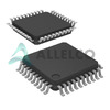
R5F21274SNFP#X6
Renesas Electronics America Inc
IC MCU 16BIT 16KB FLASH 32LQFP
1N5227B
onsemi
DIODE ZENER 3.6V 500MW DO35
12102C472JAT2A
KYOCERA AVX
CAP CER 4700PF 200V X7R 1210
PZTA64
Fairchild Semiconductor
SMALL SIGNAL BIPOLAR TRANSISTOR,
XC1765ELSO8C
AMD
IC PROM SER C-TEMP 3.3V 8-SOIC
XR88C92CJ-F
MaxLinear, Inc.
IC UART FIFO DUAL 44PLCC
RT24C2X202
Bourns, Inc.
TRIMMER 2K OHM 0.75W PC PIN SIDE
DLW31SN900SQ2L
Murata Electronics
CMC 370MA 2LN 90 OHM SMD
LMK432F476ZM-T
Taiyo Yuden
CAP CER 47UF 10V Y5V 1812
MOC207R1VM
onsemi
OPTOISO 2.5KV TRANS W/BASE 8SOIC
GRM0335C1E390JD01D
Murata Electronics
CAP CER 39PF 25V C0G/NP0 0201
SE10PG-M3/84A
Vishay General Semiconductor - Diodes Division
DIODE GEN PURP 400V 1A DO220AA
RABS15M REG
Taiwan Semiconductor Corporation
BRIDGE RECT 1P 1KV 1.5A ABS-L
PI74LPT16245AEX
Diodes Incorporated
IC TXRX NON-INVERT 3.6V 48TSSOP