GC5330IZEV Digital Signal Processor: Features, Applications, Alternatives and Specifications
This guide is all about the GC5330IZEV, a smart digital chip that helps wireless systems work better. It’s used in things like cell towers, wireless repeaters, and test equipment. The GC5330IZEV can handle many wireless signals and helps improve speed, reduce noise, and make signals clearer. In this guide, you’ll learn what this chip does, how it works, and where it’s used.Catalog
GC5330IZEV Overview
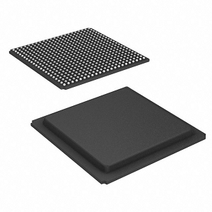
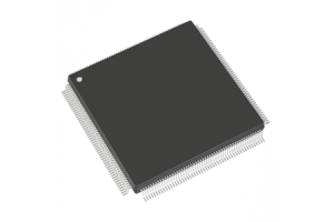
The GC5330IZEV is a sophisticated wideband transmit-receive digital signal processor (DSP), designed specifically for advanced wireless communication systems. This DSP supports a diverse range of standards such as CDMA, GSM, TD-SCDMA, W-CDMA, and WiMAX, making it highly versatile for various communication infrastructures. It features a 484-ball grid array (BGA) packaging suitable for surface-mount technology applications, ensuring seamless integration into modern electronic assemblies. Part of the broader GC5330 family, the GC5330IZEV shares a common core architecture with its siblings, aimed at optimizing the performance and efficiency of wideband transmit-receive operations.
If you're looking to lock in a dependable DSP for your systems, now’s a great time to think about placing a bulk order with us for the GC5330IZEV.
GC5330IZEV CAD Models
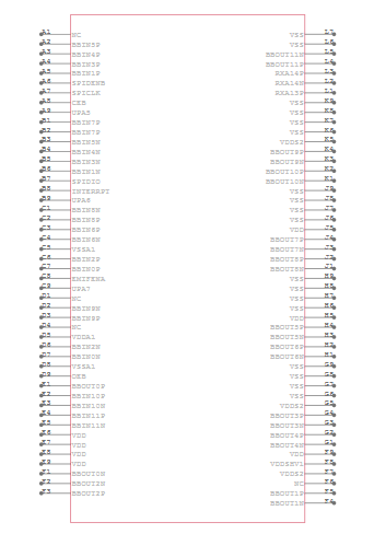
GC5330IZEV Symbol
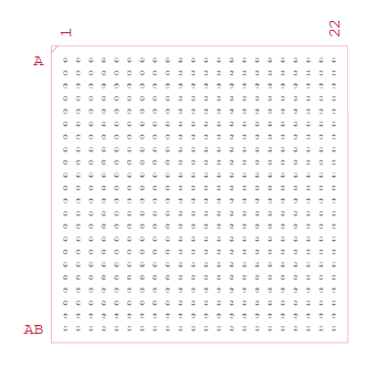
GC5330IZEV Footprint
GC5330IZEV 3D Model
GC5330IZEV Features
• Integrated Transmit and Receive Digital IF Solution: The DSP includes integrated digital upconverter (DUC) and digital downconverter (DDC) functionalities. This integration simplifies the signal processing chain by combining multiple functionalities into one compact solution, thereby reducing the complexity and size of the system.
• Multiple Channel Support: The GC5330IZEV supports up to 4 transmit (TX) and 8 receive (RX) channels. This feature enables the handling of complex multi-antenna systems, which are great for modern wireless communication technologies that require high data throughput and enhanced signal integrity.
• Transmit Path Functionalities: Key functionalities in the transmit path of the GC5330IZEV include crest factor reduction (CFR), digital predistortion (DPD), and transmit equalization. These features are need for improving the signal quality and linearity, which in turn enhances the overall efficiency and performance of communication systems.
• Synchronization Capabilities: The device is equipped with two LVDS input syncs (SYNCA and SYNCB) and one LVDS output sync. These synchronization capabilities ensure precise timing alignment across multiple devices within a system, for maintaining integrity and coherence in data transmission.
GC5330IZEV Block Diagram

The block diagram of the GC5330/GC5337 illustrates a high-performance digital transmit solution designed for base station systems. It begins with a Baseband Interface, receiving up to 24 LVDS differential pairs at 1.8V, which carry digital baseband data into the chip. This interface includes per-channel power meters and AGC (Automatic Gain Control) to ensure optimal signal levels. The Digital Down/Up Converter (DDUC) block is configurable for either transmit (TX) or receive (RX) and supports up to 12 channels. It processes the baseband signal through multiple filtering stages like FIR, Farrow, and CIC to adjust sample rates and apply interpolation or decimation. An optional Numerically Controlled Oscillator (NCO) is also included for frequency translation. Once filtered and conditioned, the signal enters the TX Path, where it is further interpolated by the CFR (Crest Factor Reduction) and DPD (Digital Pre-Distortion) blocks. These components optimize the signal's dynamic range and linearize it for efficient transmission. The ET (Envelope Tracking) and BUC (Block Up Converter) elements prepare the signal for high-frequency modulation. The IF NCO stage shifts the signal to the intermediate frequency before it's sent to the TX Format and DAC Interface, which outputs up to 4 TX streams to 8 DACs through 40 LVDS lines.
On the receive side, the system captures high-speed ADC data through 60 LVDS lines. The data is processed through DC Offset Cancellation, fe-AGC, Switch, and IF NCO blocks. It then proceeds to R2C and BDC, passing through Equalization, and optionally I/Q Imbalance Correction, before final capture and power measurement. This process supports flexible bandwidths and decimation rates. At the bottom of the diagram, several control and synchronization interfaces are shown. These include microprocessor interfaces for command and data input, JTAG for testing and debugging, and SPI for configuration. High-speed clocks and synchronization signals ensure precise timing between input, processing, and output blocks. Overall, the GC5330/GC5337 architecture is optimized for high-efficiency digital transmission with flexible configurability for various wireless standards.
GC5330IZEV Specifications
|
Type |
Parameter |
|
Manufacturer |
Texas Instruments |
|
Packaging |
Bulk |
|
Part Status |
Obsolete |
|
Function |
Digital Signal Processor |
|
RF Type |
CDMA, GSM, TD-SCDMA, W-CDMA, WiMAX |
|
Mounting Type |
Surface Mount |
|
Package / Case |
484-BGA |
|
Supplier Device Package |
484-BGA |
|
Base Product Number |
GC5330 |
GC5330IZEV Applications
Wireless Communication Systems
The GC5330IZEV is designed to handle advanced wireless protocols such as CDMA, GSM, TD-SCDMA, W-CDMA, and WiMAX. This makes it an ideal DSP for use in modern base stations and wireless infrastructure. Its integrated digital upconversion and downconversion features, along with multiple channel support, allow it to manage wideband RF signal processing efficiently. The device enhances the performance of wireless communication systems by reducing the number of required external components and offering superior signal integrity.
Wireless Repeaters
In wireless repeater applications, the GC5330IZEV serves as a bridge between receive and transmit chains. It provides digital filtering, downconversion of incoming signals, and upconversion of outgoing signals. This allows repeaters to relay communication signals over longer distances without distortion. The inclusion of features such as crest factor reduction and digital predistortion also makes it highly suitable for maintaining transmission quality in amplified paths.
Test and Measurement Equipment
The GC5330IZEV is valuable in test and measurement equipment. Its wideband processing capability and flexible channel handling allow it to simulate, process, and analyze signals across various wireless protocols. The high synchronization accuracy and advanced signal conditioning features help ensure reliable and repeatable measurements in lab and field testing environments.
Point-to-Point Radios
The GC5330IZEV is well-suited for use in point-to-point microwave and millimeter-wave radio links. In such systems, high data rate transmission and reception require DSPs capable of handling wide bandwidths and tight synchronization. This device supports those needs with its efficient digital processing, enabling reliable communication in fixed wireless access, backhaul networks, or specialized industrial links.
GC5330IZEV Similar Parts
GC5330IZEV Advantages
Enhanced Power Amplifier Efficiency
The GC5330IZEV offers improvements in overall system efficiency by incorporating Crest Factor Reduction (CFR) and Digital Predistortion (DPD). These technologies work together to reduce the peak-to-average ratio (PAR) of RF signals and correct nonlinearities in power amplifiers. As a result, amplifiers operate more efficiently, reducing power consumption and heat generation. This leads to cost savings for system operators and extends the operational lifespan of RF components.
Flexible System Integration
Thanks to its support for various MIMO configurations like 2×2, 4×4, or even 4×8, and compatibility with multiple wireless standards such as GSM, CDMA, TD-SCDMA, W-CDMA, and WiMAX, the GC5330IZEV is incredibly versatile. You can use a single platform across different communication infrastructure types, reducing development complexity, time-to-market, and the need to manage multiple DSP solutions for different networks.
Reduced Component Count and Cost
By integrating multiple processing functions such as digital upconversion, downconversion, and transmit equalization into a single device, the GC5330IZEV minimizes the need for external supporting components. This not only simplifies the PCB layout but also reduces bill-of-material (BOM) costs and system footprint. The end result is a more compact, cost-effective design that’s easier to manufacture and maintain.
Improved Signal Quality and Reliability
With built-in advanced signal processing such as CFR, DPD, and transmit equalization, the GC5330IZEV enhances signal clarity and reduces adjacent-channel leakage. This results in a more robust and interference-resistant communication channel, ensuring users receive consistent and high-quality transmission even in dense RF environments or high-data-rate scenarios.
GC5330IZEV Programming Steps
1. Interface Selection: The initial step in programming the GC5330IZEV involves selecting the appropriate communication interface. This device supports both a Microprocessor Unit (MPU) interface and a Serial Peripheral Interface (SPI). The choice depends on the system's architecture and data control requirements.The SPI interface becomes active only when the EMIFENA (External Memory Interface Enable) pin is set to logic low. You must ensure the correct hardware configuration is in place before beginning communication. This decision determines how control commands, configuration data, and status information are exchanged between the host controller and the GC5330.
2. Clock Configuration: Once the interface is established, the next step is to configure the clock signals. The GC5330IZEV operates using two main clocks: the Digital Pre-Distortion clock (DPDCLK) and the Baseband clock (BBCLK). These clocks drive the internal data processing pipeline. The DPDCLK supports frequencies up to 310 MHz, while BBCLK supports up to 290 MHz. Both must be accurately configured to meet the bandwidth and timing requirements of the intended wireless communication standard. Proper synchronization between these clock domains ensures that the signal processing stages such as filtering, interpolation, and mixing function reliably and within specification.
3. Synchronization: Synchronization is important for time-aligned operation across various modules within the GC5330IZEV. The chip provides input sync signals SYNCA and SYNCB, as well as an output synchronization signal SYNCOUT. These signals are used to align internal events such as power metering, signal capture, or DPD updating. In multi-chip or multi-channel systems, external hardware or baseband processors must coordinate sync pulses to ensure consistent processing windows. By programming the sync control registers, you can customize how and when synchronization triggers occur, ensuring stable operation even under dynamic system conditions.
4. Data Formatting: The GC5330IZEV offers flexible data formatting options for both its transmit and receive paths. You must configure the baseband input formatter for transmission and the baseband output formatter for reception. This involves selecting the appropriate data widths and formats, such as serial, byte-parallel, or nibble-parallel modes. Correct data formatting ensures compatibility with the baseband processor or FPGA handling digital I/Q streams. Programmable framing options allow for customized alignment markers and data encapsulation for systems that use complex framing structures or employ dynamic burst transmissions.
5. DUC and DDC Configuration: A major function of the GC5330IZEV is its digital upconversion (DUC) and downconversion (DDC) capability. These blocks are configured to manage signal interpolation, decimation, filtering, and frequency translation. On the transmit side, the DUC increases the sample rate and shifts the signal to the desired frequency band, ready for RF conversion. On the receive side, the DDC lowers the sample rate and filters out undesired frequency components. Proper DUC and DDC settings are good for optimizing signal fidelity, reducing aliasing, and ensuring efficient bandwidth usage. Configuration parameters include interpolation/decimation rates, filter coefficients, and mixer settings.
6. Gain Control: Automatic Gain Control (AGC) in the GC5330IZEV is split into two key areas: the front-end AGC (feAGC) and the back-end AGC (beAGC). These blocks help maintain optimal signal levels as signals move through the processing chain. The feAGC primarily deals with the incoming signal level, adjusting gain to prevent saturation or clipping. The beAGC focuses on the processed signal, ensuring it remains within expected dynamic ranges for subsequent digital operations. You must program AGC thresholds, attack/decay rates, and gain steps to handle varying signal conditions such as fading, interference, or changes in signal power.
7. Power Metering and Alarm Setup: The GC5330IZEV includes programmable power metering units capable of monitoring of signal levels. These meters help detect abnormalities such as power surges, drops, or out-of-band emissions. Programmable alarms can be configured to trigger based on preset thresholds, enabling protective or corrective action such as gain adjustments or error signaling. You must configure the metering blocks by setting power window sizes, threshold levels, and filter settings. This functionality is important in systems requiring high reliability, such as base stations, that require regulatory compliance and operational safety.
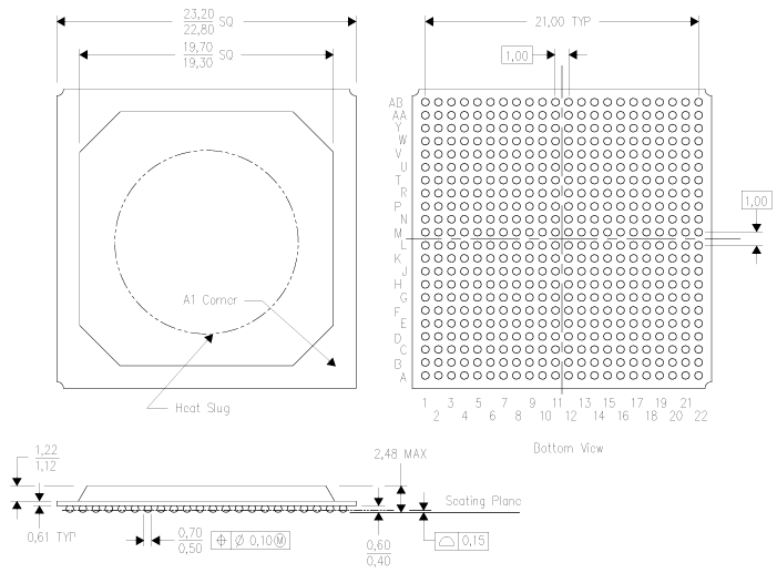
GC5330IZEV Packaging Dimensions
Package Dimensions
|
Parameter |
Dimension (mm) |
|
Body Size (Overall) |
22.80 – 23.20 |
|
Substrate Size (Inner Square) |
19.30 – 19.70 |
|
Ball Pitch (Typical) |
1 |
|
Number of Balls |
22 × AB (Grid Array) |
|
Package Height (Body) |
1.12 – 1.22 |
|
Maximum Package Height (Overall) |
2.48 |
|
Ball Diameter |
0.50 – 0.70 |
|
Ball Height Above Seating Plane |
0.40 – 0.60 |
|
Ball Diameter Tolerance |
±0.10 |
|
Ball Stand-Off (Seating Plane) |
0.15 |
Package Outline
GC5330IZEV Manufacturer
The GC5330IZEV is manufactured by Texas Instruments, a globally renowned leader in the design and production of analog and embedded processing semiconductors. Headquartered in Dallas, Texas, Texas Instruments (TI) has a long-standing reputation for innovation and reliability in the electronics industry, serving diverse sectors including automotive, industrial, communications, and consumer electronics. TI is known for its robust portfolio of high-performance integrated circuits, and the GC5330IZEV exemplifies the company's expertise in delivering complex digital radio solutions. With a focus on quality, scalability, and support for emerging communication standards, Texas Instruments ensures that components like the GC5330IZEV meet the demanding requirements of modern RF and baseband processing applications.
Conclusion
The GC5330IZEV stands out as a high-performance DSP solution engineered to meet the rigorous demands of next-generation wireless infrastructure. Its flexible channel support, integrated processing blocks, and robust synchronization make it ideal for reducing system complexity, improving power amplifier efficiency, and enhancing signal fidelity. Backed by Texas Instruments’ reputation for reliability and innovation, the GC5330IZEV is a go-to choice, aiming to build scalable and efficient RF systems with minimal component overhead.
About us
ALLELCO LIMITED
Read more
Quick inquiry
Please send an inquiry, we will respond immediately.
Frequently Asked Questions [FAQ]
1. Is the GC5330IZEV compatible with custom FPGA-based systems?
Yes, the GC5330IZEV is highly compatible with custom FPGA-based systems. Its configurable digital interfaces and data formatting options make it easy to integrate with programmable logic platforms. You can use LVDS data links, SPI, or microprocessor interfaces to communicate between your FPGA and the DSP chip, ensuring seamless signal processing in applications like base stations or test equipment.
2. How does the GC5330IZEV improve signal quality compared to discrete DSP setups?
Unlike traditional setups that rely on multiple discrete DSP components, the GC5330IZEV consolidates key features such as crest factor reduction (CFR), digital predistortion (DPD), and advanced filtering. This integration ensures tighter control over signal integrity, lower latency, and better synchronization, directly leading to improved error vector magnitude (EVM) and reduced adjacent channel interference.
3. Can the GC5330IZEV be used in 5G sub-6 GHz systems?
While the GC5330IZEV was primarily designed for 3G and 4G wireless standards, it can still serve as a powerful processing block in sub-6 GHz 5G systems that don’t require ultra-low latency or massive MIMO scalability. Its high bandwidth support and multiple TX/RX channels can help process wideband signals and support fixed wireless access or backhaul in transitional 5G deployments.
4. Can I use the GC5330IZEV for multi-band or carrier aggregation systems?
Yes, the GC5330IZEV can support multi-band systems through its multi-channel digital processing architecture. It can simultaneously handle up to 4 TX and 8 RX channels, which allows implementation of carrier aggregation across frequency bands, especially in scenarios requiring digital IF for RF front ends. Careful clocking and synchronization settings are necessary for optimal performance.
5. Can I use the GC5330IZEV in systems with software-defined radios (SDRs)?
Yes. The GC5330IZEV is compatible with SDR architectures, especially those that need a dedicated hardware DSP for intensive baseband processing. Its real-time digital conversion and channelization features allow offloading compute-heavy tasks from the general processor in an SDR environment.
EPF8820AQC208-4 FPGA: Features, Specifications, Programming, and Datasheet
on April 1th

EP1C4F324C7N FPGA: Datasheet, Features, Programming and Specifications
on April 1th
Popular Posts
-

Complex Instruction Set Computers: How They Changed Computing?
on April 17th 147713
-

USB-C Pinout and Features
on April 17th 111738
-

Using Xilinx Unified Simulation Primitives: A Comprehensive Guide to FPGA Design and Simulation
on April 17th 111322
-

Power Supply Voltages in Electronics: Meaning of VCC, VDD, VEE, VSS, and GND
on April 17th 83631
-

RJ45 Connector Guide: Pinout, Wiring, Cable Types, and Uses
on January 1th 79282
-

The Ultimate Guide to Wire Color Codes in Modern Electrical Systems
The way our electrical systems use colors isn’t just for looks. Each wire color now indicates a specific function, making it easier to identify and handle electrical components correctly during ins...on January 1th 66785
-

Quality (Q) Factor: Equations and Applications
The quality factor, or 'Q', is important when checking how well inductors and resonators work in electronic systems that use radio frequencies (RF). 'Q' measures how well a circuit minimizes energy...on January 1th 62949
-

Purge Valve Guide: Function, Symptoms, Testing, and Replacement for Optimal Engine Performance
The purge valve is a key part of a car’s system that helps keep the air clean by managing fuel vapors before they can escape into the atmosphere. This not only helps the environment by reducing pol...on January 1th 62836
-

Achieving Peak Performance with the Maximum Power Transfer Theorem
The Maximum Power Transfer Theorem explains how energy from a source, such as a battery or generator, flows to a connected load. It shows the exact condition where the load receives the most power....on January 1th 54036
-

A23 Battery Specifications and Compatibility
The A23 battery is a small, cylinder-shaped battery with high voltage. Also called 23A, 23AE, or MN21, it runs at 12 volts and much higher than AA or AAA batteries. Its special design make...on January 1th 52003
HOT Part Number
-
R1240K003A-TR
Nisshinbo Micro Devices Inc.
1.2A 30V INPUT PWM STEP-DOWN DCD
SM6T36AY
STMicroelectronics
TVS DIODE 30.8VWM 64.3VC SMB
MC10EP01DR2G
onsemi
IC GATE OR/NOR ECL 4INPUT 8-SOIC
XC2V3000-5BF957I
AMD
IC FPGA 684 I/O 957FCBGA
1-1827875-3
TE Connectivity AMP Connectors
CONN HEADER VERT 6POS 2.5MM
MAX2363EGM-TD
Analog Devices Inc./Maxim Integrated
DUAL-BAND QUADRATURE TRANSMITTER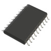
AD7849BRZ
Analog Devices Inc.
IC DAC 16BIT V-OUT 20SOIC
CRCW08054R70FKEAHP
Vishay Dale
RES SMD 4.7 OHM 1% 1/2W 0805
1.5SMC33CA
Taiwan Semiconductor Corporation
TVS DIODE 28.2VWM 45.7VC DO214AB
S9S08DZ16F2MLF
Freescale Semiconductor
IC MCU 8BIT 16KB FLASH 48LQFP
TPS53915RVER
Texas Instruments
IC REG BUCK ADJ 12A 28VQFN
ICM7556IPD
Harris Corporation
TRANSISTOR RC TIMER, 2 FUNC, 1MH
STS11NF30L
STMicroelectronics
MOSFET N-CH 30V 11A 8SO
ATF16LV8C-15XC
Microchip Technology
IC PLD 8MC 15NS 20TSSOP
PIC16F84-10I/P
Microchip Technology
IC MCU 8BIT 1.75KB FLASH 18DIP
HEF40175BT,652
NXP Semiconductors
NEXPERIA HEF40175BT - D FLIP-FLO
AO4838
Alpha & Omega Semiconductor Inc.
MOSFET 2N-CH 30V 11A 8SOIC
AON7423
Alpha & Omega Semiconductor Inc.
MOSFET P-CH 20V 28A/50A 8DFN -
SE5005L-R
Skyworks Solutions Inc.
IC AMP 802.11A 5.75GHZ 16QFN
TPS2051DR
Texas Instruments
IC PWR SWITCH N-CHAN 1:1 8SOIC
BCX38C
Diodes Incorporated
TRANS NPN DARL 60V 0.8A TO92
PIC16LC505-04I/SL
Microchip Technology
IC MCU 8BIT 1.5KB OTP 14SOIC
BC848BHZGT116
Rohm Semiconductor
TRANS NPN 30V 0.1A SST3
EL1517ILZ-T7
Renesas Electronics America Inc
IC DRIVER 1/0 16QFN
FS32K146HFT0VLHR
NXP USA Inc.
IC MCU 32BIT 1MB FLASH 64LQFP
BZT52C20
Diotec Semiconductor
ZENERDIODE,SOD-123,20V,0.5W,5%
MCP7940N-I/SN
Microchip Technology
IC RTC CLK/CALENDAR I2C 8SOIC
NTTS2P02R2G
onsemi
MOSFET P-CH 20V 2.4A MICRO8
UA78L09ACPK
Texas Instruments
IC REG LINEAR 9V 100MA SOT89-3
06031C271M4Z2A
KYOCERA AVX
CAP CER 270PF 100V X7R 0603
EMK105SD152KV-F
Taiyo Yuden
CAP CER 1500PF 16V 0402
DAC904E/2K5
Texas Instruments
IC DAC 14BIT A-OUT 28TSSOP
8869430000
Weidmüller
RELAY SOCKET 14 POS DIN RAIL
BQ296222DSGR
Texas Instruments
IC BATT PROT LI-ION 2-4CEL 8WSON
LT1361CS8#PBF
Analog Devices Inc.
IC VOLTAGE FEEDBACK 2 CIRC 8SO
AD524ARZ-16-REEL7
Analog Devices Inc.
IC INST AMP 1 CIRCUIT 16SOIC -
ACPL-P346-500E
Broadcom Limited
OPTOISO 3.75KV 1CH GATE DRVR 6SO
SN74LVC240ADGVR
Texas Instruments
IC BUFFER INVERT 3.6V 20TVSOP
AT24C128B-TH-B
Microchip Technology
IC EEPROM 128KBIT I2C 8TSSOP
1812GC272MAT1A\SB
KYOCERA AVX
CAP CER 2700PF 2KV X7R 1812
LD2981ABM25TR
STMicroelectronics
IC REG LINEAR 2.5V 100MA SOT23-5
74LCX646MTCX
Fairchild Semiconductor
IC TXRX NON-INVERT 3.6V 24TSSOP
Z84C4006PEG
Zilog
IC INTERFACE SPECIALIZED 40DIP
LD2981ABM33TR
STMicroelectronics
IC REG LINEAR 3.3V 100MA SOT23-5
AR0140AT3C00XUEA0-DPBR
onsemi
IMAGE SENSOR
SURS8320T3G
onsemi
DIODE GEN PURP 200V 3A SMC
DAC70004IDMDR
Texas Instruments
IC DAC 14BIT V-OUT 14VSON
AT34C02D-XHMHL-T
Microchip Technology
IC EEPROM 2KBIT I2C 1MHZ 8TSSOP
ADG509AKP
Analog Devices Inc.
IC SWITCH SP4T X 2 450OHM 20PLCC
LM22671MR-ADJ
Texas Instruments
SWITCHING REGULATOR, VOLTAGE-MOD
NRVBA340T3G-VF01
onsemi
DIODE SCHOTTKY 40V 3A SMA
FX10A-168P-SV(83)
Hirose Electric Co Ltd
CONN HDR 168POS SMD GOLD
C1005C0G1H390J/50
TDK Corporation
CAP CER 39PF 50V C0G 0402
AO6602G
Alpha & Omega Semiconductor Inc.
COMPLEMENTARY