Lattice LFEC3E-3QN208C FPGA Guide: Features, Datasheet and Alternatives
If you’re working on projects that need reliable logic control without going over budget, the LFEC3E-3QN208C FPGA is worth knowing. It gives you the right mix of logic, memory, and I/O flexibility in a compact package. In this guide, you’ll see its main features, how it works inside, where you can use it, how to program it, and what advantages and limits to expect.Catalog
What is the LFEC3E-3QN208C?
The LFEC3E-3QN208C is an FPGA device from Lattice Semiconductor’s EC/ECP family, designed as part of the company’s economy-class programmable logic series. Built to balance cost efficiency with reliable performance, this device offers a scalable architecture for digital logic implementation. The “QN208C” suffix identifies its compact 208-pin package, making it suitable for integration where board space is a concern. As a member of the mature LatticeEC/ECP family, it carries the hallmarks of flexibility and trusted design found in this product line.
Looking for LFEC3E-3QN208C? Contact us to check current stock, lead time, and pricing.
LFEC3E-3QN208C Features
• Logic Capacity
The LFEC3E-3QN208C provides around 3,100 logic elements, which can be used to implement digital circuits, state machines, and custom datapaths. This level of density is suitable for mid-range designs such as communications interfaces, industrial control, and embedded processing.
• On-Chip Memory
It integrates about 56,320 bits of block RAM and distributed RAM, allowing to store data buffers, lookup tables, or small FIFOs directly inside the FPGA. This reduces reliance on external memory for many moderate-size data tasks.
• I/O Resources
Housed in a 208-pin QFP package, the device supports around 140+ user I/O pins depending on the configuration. This makes it flexible for applications requiring multiple interfaces, parallel buses, or mixed-signal connectivity.
• Operating Voltage
The core operates at approximately 1.2 V, with I/O banks supporting multiple voltage standards from 1.2 V to 3.3 V. This wide compatibility enables the FPGA to interface with both modern low-voltage logic and legacy 3.3 V systems.
• System Clocking
The device includes on-chip PLLs (sysCLOCK™) that can multiply, divide, or phase-shift input clocks. This allows to generate precise internal clocks for DDR interfaces, high-speed data paths, and synchronized logic domains.
• Memory Interface Support
LFEC3E-3QN208C supports DDR SDRAM interfaces up to DDR-400 (200 MHz clock). This gives it the ability to connect directly to external memory chips for higher-capacity storage or buffering in data-intensive applications.
• I/O Standards
It supports a wide range of industry-standard signaling protocols, including LVCMOS, LVTTL, SSTL, HSTL, PCI, and LVDS. This ensures compatibility with a broad set of processors, ASICs, and communication interfaces.
• In-System Programmability
The FPGA can be programmed via JTAG (IEEE 1149.1) and supports in-system reconfiguration. This makes development, debugging, and field upgrades straightforward without removing the device from the PCB.
• Debug and Analysis
It provides support for Lattice’s ispTRACY logic analyzer, which probe internal signals in time. This feature simplifies debugging complex logic designs without the need for external probes.
• Lifecycle Status
The LFEC3E-3QN208C belongs to the Lattice EC family, which is now considered a mature or discontinued product line.
LatticeEC Block Diagram
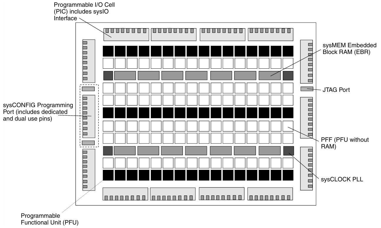
The block diagram of the LatticeEC FPGA family (like LFEC3E-3QN208C) shows how its internal architecture is organized to balance logic, memory, and connectivity. Around the edges are programmable I/O cells (PICs), which handle communication with external devices and support multiple voltage standards for flexible interfacing. Inside, the grid is filled with programmable functional units (PFUs), where user logic is implemented, while dedicated sysMEM embedded block RAMs (EBRs) provide high-speed memory for buffering and data storage. System resources include sysCLOCK PLLs, which manage clock generation and synchronization, ensuring stable high-performance operation, and the sysCONFIG/JTAG ports, which allow in-system programming and testing. This arrangement makes the FPGA versatile, combining reconfigurable logic, embedded memory, and robust I/O for a wide range of applications in communications, control, and embedded systems.
LatticeEC Banks Diagram
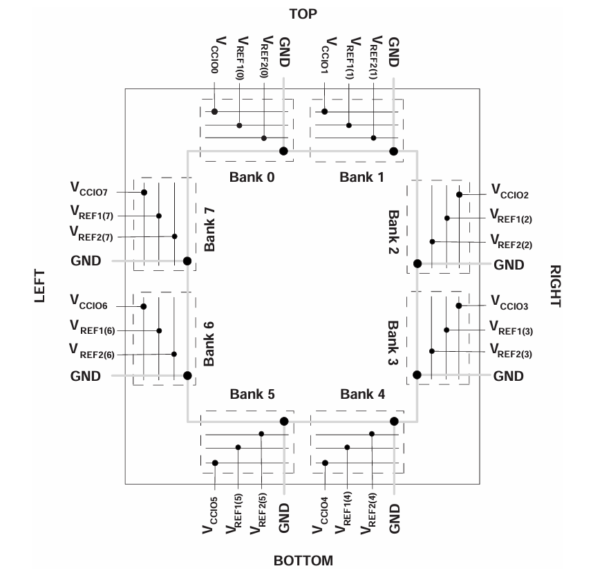
The LatticeEC banks diagram for devices like the LFEC3E-3QN208C illustrates how the FPGA’s I/O pins are organized into eight banks, each with its own supply and reference voltages. Every bank can be powered independently through its VCCIO pins, allowing the FPGA to support multiple I/O voltage standards (such as 1.2 V, 1.8 V, 2.5 V, or 3.3 V) simultaneously. Each bank also includes VREF pins, which are great for certain standards like SSTL and HSTL that require reference voltages to set proper logic thresholds. This modular structure gives flexibility to interface the FPGA with different external components such as processors, memory, and peripherals without level shifters. The banked architecture enhances the product’s versatility and makes it easier to integrate into mixed-voltage systems, a key advantage in industrial and communication applications.
LFEC3E-3QN208C Specifications
|
Type |
Parameter |
|
Manufacturer |
Lattice Semiconductor Corporation |
|
Series |
EC |
|
Packaging |
Tray |
|
Part Status |
Obsolete |
|
Number of Logic Elements/Cells |
3100 |
|
Total RAM Bits |
56,320 |
|
Number of I/O |
145 |
|
Voltage – Supply |
1.14V ~ 1.26V |
|
Mounting Type |
Surface Mount |
|
Operating Temperature |
0°C ~ 85°C (TJ) |
|
Package / Case |
208-BFQFP |
|
Supplier Device Package |
208-PQFP (28×28) |
|
Base Product Number |
LFEC3 |
LFEC3E-3QN208C Applications
1. Embedded Control Systems
The LFEC3E-3QN208C can serve as the central logic controller in industrial automation, robotics, or motor control systems. Its reprogrammable architecture allows to implement custom state machines and timing-critical logic without redesigning hardware. With low core voltage and multiple I/O banks, it integrates seamlessly with both modern sensors and traditional controllers. This makes it ideal for reliable, time embedded control solutions.
2. Interface Bridging / Protocol Conversion
Because the FPGA supports multiple I/O standards and voltage levels, it can serve as a bridge between different communication protocols. For example, it can translate between legacy buses (such as PCI or parallel interfaces) and newer standards like LVDS or DDR memory. This capability helps extend the life of existing systems while allowing the integration of new devices. Such flexibility reduces the need for external glue logic and accelerates system integration.
3. Signal Processing in Communications
The LFEC3E-3QN208C is capable of handling basic DSP tasks, including filtering, error detection, or packet handling in communication systems. Its embedded block RAM and logic cells provide efficient resources for buffering and managing data streams. By offloading these functions from a microprocessor, overall system throughput and responsiveness improve. This makes it suitable for wireless modules, small-scale base stations, and networking equipment.
4. Test, Measurement & Instrumentation
In test and measurement equipment such as oscilloscopes, data loggers, or logic analyzers, the FPGA can be configured to capture, filter, and preprocess data in time. Its programmable I/O banks allow direct connection to various signal levels without extra conversion circuitry. By leveraging its embedded RAM, temporary data can be stored and forwarded to external processors efficiently. This capability improves accuracy and reduces latency in instrumentation applications.
5. Prototyping and Custom Hardware Accelerators
The device can also serve as a platform for hardware prototyping or small-scale accelerators. It can implement encryption blocks, checksum generators, or other compute-intensive tasks directly in logic. This shortens the development cycle compared to ASICs and enables rapid modifications in the field. For research, startups, and custom embedded solutions, it offers a cost-effective entry point into FPGA-based acceleration.
LFEC3E-3QN208C Similar Parts
|
Specification |
LFEC3E-3QN208C |
LFEC3E-3QN208I |
LFEC3E-3Q208I |
LFEC3E-3TN100C |
LFEC3E-3TN144C |
LFEC3E-3FN256C |
|
Logic Elements / Cells |
3,100 |
3,100 |
3,100 |
3,100 |
3,100 |
3,100 |
|
Embedded Memory (bits) |
56,320 |
56,320 |
56,320 |
56,320 |
56,320 |
56,320 |
|
Max Operating Frequency |
~340 MHz |
~340 MHz |
~340 MHz |
~340 MHz |
340 MHz |
340 MHz |
|
Number of I/Os |
145 |
145 |
145 |
~80–90 |
97 |
160 |
|
Core Voltage Range |
1.14 V – 1.26 V |
1.14 V – 1.26 V |
1.14 V – 1.26 V |
1.14 V – 1.26 V |
1.14 V – 1.26 V |
1.14 V – 1.26 V |
|
Operating Temperature |
0 °C to 85 °C |
0 °C to 85 °C |
0 °C to 85 °C |
0 °C to 85 °C |
0 °C to 70 °C |
0 °C to 85 °C |
|
Package Type |
208-pin QFP |
208-pin QFP |
208-pin QFP |
100-pin TQFP |
144-pin TQFP |
256-ball BGA |
|
Lifecycle Status |
Obsolete |
Obsolete |
Obsolete |
Obsolete |
Obsolete |
Obsolete |
|
I/O Standards Supported |
LVCMOS, LVTTL, LVDS, SSTL, HSTL, PCI |
Same |
Same |
Limited (fewer banks) |
Same set, fewer pins |
Full set with more banks |
|
External Memory Support |
DDR up to DDR-400 |
DDR up to DDR-400 |
DDR up to DDR-400 |
DDR up to DDR-400 |
DDR up to DDR-400 |
DDR up to DDR-400 |
LFEC3E-3QN208C Programming Steps
Before you can use the LFEC3E-3QN208C FPGA, you need to program it with your custom design. The process involves creating your logic design, generating a bitstream, and transferring it into the chip through supported interfaces.
1. Design & Bitstream Generation
You start by writing your design in HDL (Verilog or VHDL) and then compile it using Lattice’s development tools like ispLEVER or Diamond. During this process, you’ll synthesize the logic, perform placement and routing, and apply I/O and timing constraints. The tool then produces a bitstream file (.bit or .jed), which contains all the configuration data required by the FPGA. This file is what you’ll later transfer into the device to bring your design to life.
2. Choose the Configuration Mode
Next, you must decide how the FPGA will load its configuration. The LFEC3E-3QN208C supports multiple modes, such as JTAG programming for direct download or sysCONFIG modes like serial or parallel boot from external flash memory. You select the mode by setting the device’s configuration pins (CFG[2:0]) or by wiring it appropriately to external memory. Choosing the right mode depends on whether you want quick prototyping or a permanent, power-up configuration.
3. Connect the Programming Interface
After choosing the mode, you connect the proper programming hardware. For JTAG, you’ll use a download cable or programmer linked to the FPGA’s JTAG pins. If you’re using sysCONFIG, an external flash or microcontroller will act as the configuration source. Ensuring proper wiring, pin assignments, and power sequencing at this stage is good for reliable programming.
4. Load the Configuration
With the hardware in place, you now transfer the bitstream into the FPGA. The programmer sends the data through the JTAG or sysCONFIG interface, and the FPGA writes it into its internal configuration memory. During this process, the device checks the data integrity using CRC and signals success by asserting the DONE pin high. At this point, your design becomes active, and the FPGA begins operating as you programmed it.
5. Runtime & Reconfiguration
Finally, you have the option to reconfigure the device without removing it from the system. Using JTAG or sysCONFIG again, you can update the FPGA with a new bitstream if your design changes. This ability is useful for field upgrades or iterative testing. By taking advantage of in-system programmability, you ensure your LFEC3E-3QN208C can adapt to evolving requirements over time.
LFEC3E-3QN208C Advantages and Disadvantages
Advantages
• Low-cost FPGA option for budget-sensitive designs
• Low power consumption compared to many alternatives
• Balanced resources without over-design overhead
• Strong legacy ecosystem and proven reliability
• Flexible configuration via JTAG or sysCONFIG modes
Disadvantages
• Lower performance ceiling than high-end FPGAs
• Limited logic density and memory capacity
• Risk of obsolescence as part of a mature/discontinued line
• Lacks advanced features like DSP blocks or SERDES
• Power/performance trade-offs at higher utilization
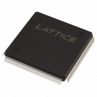
LFEC3E-3QN208C Packaging Dimensions
|
Type |
Parameter |
|
Package Type |
208-PQFP (Plastic Quad Flat Pack) |
|
Body Size (L × W) |
28 mm × 28 mm |
|
Package Height (Max) |
3.40 mm |
|
Pitch (Lead Spacing) |
0.50 mm |
|
Number of Pins |
208 |
|
Lead Length (L) |
0.45 mm ~ 0.75 mm |
|
Lead Width (b) |
0.17 mm ~ 0.27 mm |
|
Overall Lead Span (D/E) |
30 mm ~ 30.5 mm |
|
Seating Plane (A1) |
0.05 mm ~ 0.15 mm |
|
Package Code |
BFQFP-208 / PQFP-208 |
LFEC3E-3QN208C Manufacturer
LFEC3E-3QN208C is manufactured by Lattice Semiconductor Corporation, a leading provider of low-power, small-form-factor programmable logic devices. Founded in 1983 and headquartered in Hillsboro, Oregon, USA, Lattice focuses on delivering cost-effective FPGA and CPLD solutions tailored for communications, computing, industrial, automotive, and consumer applications. The company is recognized for its emphasis on low-power architectures, flexible I/O standards, and solutions that extend product lifecycles for embedded and industrial markets. With a global presence in design, support, and distribution, Lattice Semiconductor continues to provide developers with reliable, efficient, and reprogrammable platforms that meet both current and legacy system demands.
Conclusion
The LFEC3E-3QN208C offers a practical combination of logic density, embedded memory, versatile I/O, and in-system programmability, making it well-suited for embedded control, communications, prototyping, and instrumentation. Its support for multiple standards and flexible voltage banks ensures compatibility with both modern and legacy systems. While it provides low power consumption, cost-effectiveness, and reliability, it does come with trade-offs such as limited performance and potential obsolescence. Overall, the device remains a dependable choice for those seeking a balanced FPGA for a wide range of industrial and embedded applications.
Datasheet PDF
LFEC3E-3QN208C Datasheets:
About us
ALLELCO LIMITED
Read more
Quick inquiry
Please send an inquiry, we will respond immediately.
Frequently Asked Questions [FAQ]
1. What tools do I need to program the LFEC3E-3QN208C FPGA?
You can program it using Lattice ispLEVER Classic or Diamond software, combined with a JTAG cable or sysCONFIG setup. These tools support design synthesis, simulation, bitstream generation, and in-system programming.
2. Does the LFEC3E-3QN208C support low-power applications?
Yes, its 1.2 V core and flexible I/O voltages make it a good fit for low-power systems. It’s particularly effective in battery-powered or energy-sensitive designs compared to many high-performance FPGAs.
3. Can I use the LFEC3E-3QN208C for DDR2 or DDR3 memory?
No, this FPGA officially supports DDR SDRAM up to DDR-400. For DDR2/DDR3 compatibility, newer FPGA families are recommended, as they include more advanced memory controllers.
4. What’s the maximum operating temperature for the LFEC3E-3QN208C?
It is typically available in commercial (0°C to +70°C) and industrial (-40°C to +85°C) temperature ranges. Always check the datasheet for the exact part ordering code to ensure the right grade.
5. How does the LFEC3E-3QN208C compare to high-end FPGAs in terms of performance?
It delivers reliable performance for mid-range applications but lacks advanced features like SERDES, DSP slices, or very high logic density. If you need those, higher-end Lattice or competitor FPGAs like Xilinx or Intel devices are better suited.

OP400HS Precision Quad Op Amp: Features, Pinout, Applications, and Alternatives
on October 2th

ADV7123JST240 Video DAC: Datasheet, Features, Applications, and Alternatives
on September 28th
Popular Posts
-

Complex Instruction Set Computers: How They Changed Computing?
on April 18th 147749
-

USB-C Pinout and Features
on April 18th 111916
-

Using Xilinx Unified Simulation Primitives: A Comprehensive Guide to FPGA Design and Simulation
on April 18th 111349
-

Power Supply Voltages in Electronics: Meaning of VCC, VDD, VEE, VSS, and GND
on April 18th 83714
-

RJ45 Connector Guide: Pinout, Wiring, Cable Types, and Uses
on January 1th 79502
-

The Ultimate Guide to Wire Color Codes in Modern Electrical Systems
The way our electrical systems use colors isn’t just for looks. Each wire color now indicates a specific function, making it easier to identify and handle electrical components correctly during ins...on January 1th 66872
-

Quality (Q) Factor: Equations and Applications
The quality factor, or 'Q', is important when checking how well inductors and resonators work in electronic systems that use radio frequencies (RF). 'Q' measures how well a circuit minimizes energy...on January 1th 63005
-

Purge Valve Guide: Function, Symptoms, Testing, and Replacement for Optimal Engine Performance
The purge valve is a key part of a car’s system that helps keep the air clean by managing fuel vapors before they can escape into the atmosphere. This not only helps the environment by reducing pol...on January 1th 62948
-

Achieving Peak Performance with the Maximum Power Transfer Theorem
The Maximum Power Transfer Theorem explains how energy from a source, such as a battery or generator, flows to a connected load. It shows the exact condition where the load receives the most power....on January 1th 54077
-

A23 Battery Specifications and Compatibility
The A23 battery is a small, cylinder-shaped battery with high voltage. Also called 23A, 23AE, or MN21, it runs at 12 volts and much higher than AA or AAA batteries. Its special design make...on January 1th 52091
HOT Part Number
-

BD9B100MUV-E2
Rohm Semiconductor
IC REG BUCK ADJ 1A 16VQFN
UPD70F3539AF5A9-PN7-Q-A
Renesas Electronics America Inc
IC MICROCONTROLLER
18081A621JAT2A
KYOCERA AVX
CAP CER 620PF 100V NP0 1808
FDN340P
onsemi
MOSFET P-CH 20V 2A SUPERSOT3
70231-101
Amphenol ICC (FCI)
CONN RCPT BLADE PWR 8POS EDGE MT
MPSW42RLRAG
onsemi
TRANS NPN 300V 0.5A TO92
MC7824BT
onsemi
IC REG LINEAR 24V 1A TO220AB
AD8009ARZ-REEL
Analog Devices Inc.
IC OPAMP CFA 1 CIRCUIT 8SOIC
LT1815CS5#TRPBF
Analog Devices Inc.
IC OPAMP VFB 1 CIRCUIT TSOT23-5
DG411DYZ
Renesas Electronics America Inc
IC SWITCH SPST-NCX4 35OHM 16SOIC
VFT2060C-M3/4W
Vishay General Semiconductor - Diodes Division
DIODE SCHOTTKY 20A 60V ITO-220AB
TSX562AIYST
STMicroelectronics
IC CMOS 2 CIRCUIT 8MINISO
MR256D08BMA45
Everspin Technologies Inc.
IC RAM 256KBIT PARALLEL 48FBGA
VSC3312YYP-01
Microchip Technology
IC SWITCH 16X16 6.5GBPS 196FCBGA
XC68HC908GP20CFB
Motorola
TSG 8BIT20K FLASH
CSR8811A08-ICXR-R
Qualcomm
IC RF TXRX+MCU BLUETOOTH
MPSW05
onsemi
TRANS NPN 60V 0.5A TO92
1N4055R
Solid State Inc.
DIODE GEN PURP REV 900V 275A DO9 -

ASX342ATSC00XPED0-DP
onsemi
IMAGE SENSOR VGA 1/4 CIS SOC
0433.125NR
Littelfuse Inc.
FUSE BOARD MNT 125MA 125VAC/VDC
1SMA5941BT3G
onsemi
DIODE ZENER 47V 1.5W SMA
DCP010512BP-U/700
Texas Instruments
DC DC CONVERTER 12V 1W
1-1734344-1
TE Connectivity AMP Connectors
CONN D-SUB HD RCPT 15P R/A SLDR
KSD1621STF
onsemi
TRANS NPN 25V 2A SOT89-3
BQ24161RGET
Texas Instruments
IC BATT CHG LI-ION 1CELL 24VQFN
BTA26-600BW
STMicroelectronics
TRIAC ALTERNISTOR 600V 25A TOP3
NCP1239DD65R2G
onsemi
IC OFFLINE SWITCH FLYBACK 7SOIC
TMS320TCI6482BZTZA
Texas Instruments
TMS320 - DIGITAL SIGNAL PROCESSO
BQ20Z90DBTR-V150
Texas Instruments
IC GAS GAUGE LI-ION 30TSSOP
PCMB104T-1R0MT
Susumu
FIXED IND 1UH 18A 3.3 MOHM SMD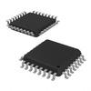
CY29942AXCT
Infineon Technologies
IC CLK BUFFER 1:18 200MHZ 32TQFP
CC0402KRX7R9BB561
YAGEO
CAP CER 560PF 50V X7R 0402
STPS20M60SG-TR
STMicroelectronics
DIODE SCHOTTKY 60V 20A D2PAK
AT25010N-10SC-2.7
Microchip Technology
IC EEPROM 1KBIT SPI 3MHZ 8SOIC
04023A1R0CAT4A
KYOCERA AVX
CAP CER 1PF 25V C0G/NP0 0402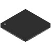
ISL6327IRZ
Intersil
SWITCHING CONTROLLER, VOLTAGE-MO -

LQW18AN75NG0ZD
Murata Electronics
FIXED IND
DFA100BA160
SanRex Corporation
DIODE MODULE 1600V 100A
BAR46AFILM
STMicroelectronics
DIODE ARRAY SCHOTTKY 100V SOT23
MAX825SEUK
Analog Devices Inc./Maxim Integrated
IC SUPERVISOR MPU
MMST2222A-7-F
Diodes Incorporated
TRANS NPN 40V 0.6A SOT323
FODM8801AR2
onsemi
OPTOISO 3.75KV TRANS 4-MINI-FLAT
FJV1845FMTF
Fairchild Semiconductor
SMALL SIGNAL BIPOLAR TRANSISTOR,
EVK105RH5R1JW-F
Taiyo Yuden
CAP CER 5.1PF 16V R2H 0402
6651170-3
TE Connectivity AMP Connectors
CONN EDGE DUAL FMALE 4POS 0.508
KSZ8893FQLI-FX
Microchip Technology
IC SWITCH ETH 3PORT 128QFP
170M6340
Eaton - Bussmann Electrical Division
FUSE SQUARE 400A 1.3KVAC RECT
BCM20741A2KFB1G
Broadcom Limited
SINGLE-CHIP BLUETOOTH
MAX3443EASA+
Analog Devices Inc./Maxim Integrated
IC TRANSCEIVER HALF 1/1 8SOIC
GRM0335C1H9R3DA01D
Murata Electronics
CAP CER 9.3PF 50V C0G/NP0 0201
TNY175PN
Power Integrations
11.5 W (85-265 VAC) 15 W (230 VA
742700726
Würth Elektronik
FERRITE CORE 278 OHM SOLID 4MM
DM74S20N
onsemi
IC GATE NAND 2CH 4-INP 14DIP
P4SMA56CA-E3/61
Vishay General Semiconductor - Diodes Division
TVS DIODE 47.8VWM 77VC DO214AC