P82B96 Bipolar IC Guide: Pin Details, 3D Model, and Datasheet Analysis
The P82B96 IC serves as a versatile solution designed to facilitate seamless communication between the I2C bus and various other bus configurations, making it a serious component in modern electronics. Its ability to support bidirectional logic-level interfacing across different voltage and current standards enhances its value in complex circuit designs. Whether used in automotive systems, industrial environments, or consumer electronics, the P82B96 enables you to ensure reliable, high-performance communication between microcontrollers, sensors, and other peripherals, regardless of varying electrical characteristics.Catalog

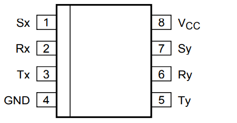
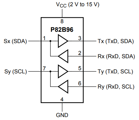
Pinout of P82B96
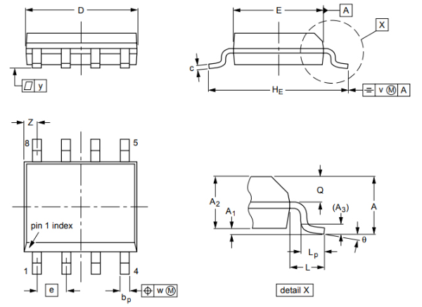
CAD Model of P82B96
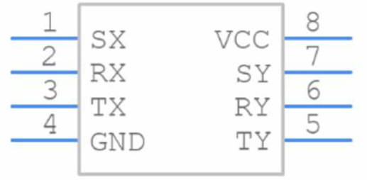
Symbol
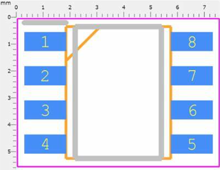
Footprint
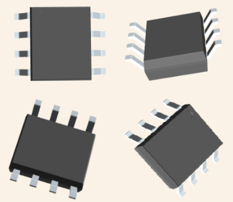
3D Model
Overview of P82B96
The P82B96 IC is crafted to offer a non-latching, bidirectional interface between the standard I2C bus and other bus configurations. This IC bridges I2C-bus logic to different buses with varying voltage and current characteristics, including the 350 µA SMBus, and 3.3V logic devices, and it even extends to 15V levels or low-impedance lines. It seamlessly manages these interfaces while maintaining the original I2C-bus protocols and clock speeds. The IC significantly alleviates the load on the I2C-bus node by isolating it from new or remote I2C-bus nodes. This isolation reduces worries about the number of devices or their physical placement in an I2C system, thus effectively removing such limitations. The P82B96 also supports transmitting SDA and SCL signals via balanced lines, such as twisted pairs or with opto-coupling, offering flexible and reliable interconnections.
You can often esteem the P82B96 for simplifying intricate I2C configurations. For instance, in settings where devices are spread over considerable distances or display diverse electrical characteristics, the P82B96 lends a practical and efficient degree of flexibility. The P82B96's versatility in supporting various applications extends beyond typical use cases. For example, in industrial automation, where rugged communication over long distances is a must, the IC’s adeptness at handling high-voltage lines without compromising I2C signal integrity is vital.
Moreover, in advanced consumer electronics, where integration density and low power consumption are the main ones, the P82B96’s minimal current draw and high voltage tolerance offer distinct advantages. You can create systems that are both compact and energy-efficient by capitalizing on the IC’s versatile interface capabilities. In telecommunications, the IC's ability to maintain signal fidelity across diverse interfacing conditions aids in developing resilient communication infrastructures.
P82B96 Characteristics
|
Feature |
Description |
|
Bidirectional
data transfer |
Enables
bidirectional data transfer of I2C-bus signals |
|
Capacitance
isolation |
Isolates
capacitance, allowing up to 400 pF on Sx/Sy side and up to 4000 pF on Tx/Ty
side |
|
High
sink capability |
Tx/Ty
outputs can sink up to 60 mA, suitable for driving low-impedance or
high-capacitance buses |
|
Long-distance
operation |
Supports
400 kHz operation over distances of at least 20 meters (refer to AN10148) |
|
Wide
supply voltage range |
Operates
with a supply voltage range of 2 V to 15 V, independent of I2C-bus logic
levels on the Sx/Sy side |
|
Signal
splitting for isolation |
Splits
I2C-bus signals into forward/reverse Tx/Rx, Ty/Ry pairs for interfacing with
opto-electrical isolators |
|
Low
power consumption |
Features
low supply current |
|
ESD
protection |
ESD
protection: exceeds 3500 V HBM, 250 V DIP, 400 V SO package MM, and 1000 V
CDM |
|
Latch-up
free operation |
Latch-up
free, built using a bipolar process without latching structures |
|
Available
packages |
Offered
in DIP8, SO8, and TSSOP8 packages |
Technical Specifications
Here is the structured table for the technical specifications of the NXP USA Inc. P82B96TD,112.
|
Type |
Parameter |
|
Factory
Lead Time |
7
Weeks |
|
Mounting
Type |
Surface
Mount |
|
Package
/ Case |
8-SOIC
(0.154, 3.90mm Width) |
|
Surface
Mount |
YES |
|
Interface
Standards |
General
Purpose |
|
Operating
Temperature |
-40°C
~ 85°C |
|
Packaging |
Tube |
|
Published |
2003 |
|
JESD-609
Code |
e4 |
|
Part
Status |
Active |
|
Moisture
Sensitivity Level (MSL) |
1
(Unlimited) |
|
Number
of Terminations |
8 |
|
Type |
Buffer,
ReDriver |
|
Terminal
Finish |
Nickel/Palladium/Gold
(Ni/Pd/Au) |
|
Applications |
I2C |
|
Voltage
- Supply |
2V ~
15V |
|
Terminal
Position |
Dual |
|
Terminal
Form |
Gull
Wing |
|
Peak
Reflow Temperature (°C) |
260 |
|
Number
of Functions |
2 |
|
Supply
Voltage |
5V |
|
Time@Peak
Reflow Temperature-Max (s) |
30 |
|
Base
Part Number |
P82B96 |
|
Output |
2-Wire
Bus |
|
Pin
Count |
8 |
|
JESD-30
Code |
R-PDSO-G8 |
|
Qualification
Status |
Not
Qualified |
|
Number
of Channels |
2 |
|
Current
- Supply |
900µA |
|
Input |
2-Wire
Bus |
|
Driver
Number of Bits |
2 |
|
Receiver
Number of Bits |
2 |
|
Data
Rate (Max) |
400kHz |
|
Capacitance
- Input |
7pF |
|
Length |
4.9mm |
|
Height
Seated (Max) |
1.75mm |
|
Width |
3.9mm |
|
RoHS
Status |
RoHS3
Compliant |
Block Diagram of P82B96
Alternatives for P82B96
|
Model Number |
Manufacturer |
Description |
|
P82B96PN,112 |
NXP
Semiconductors |
P82B96P
- Dual bidirectional bus buffer DIP 8-Pin |
|
P82B96PE4 |
Texas
Instruments |
DUAL
LINE TRANSCEIVER, PDIP8, ROHS COMPLIANT, PLASTIC, DIP-8 |
|
9.4E+11 |
NXP
Semiconductors |
IC
SPECIALTY MICROPROCESSOR CIRCUIT, PDIP8, DIP-8, Microprocessor IC: Other |
|
P82B96P
|
Texas
Instruments |
2-bit
bidirectional 2- to 15-V 400-kHz I2C/SMBus buffer/cable extender 8-PDIP -40
to 85°C |
Comparable Products
|
Part Number |
Manufacturer |
Package / Case |
Supply Voltage |
Input |
Moisture Sensitivity Level (MSL) |
Factory Lead Time |
Length |
Output |
Pin Count |
View Compare |
|
P82B96TD,112 |
NXP
USA Inc. |
8-SOIC
(0.154, 3.90mm Width) |
5 V |
2-Wire
Bus |
1
(Unlimited) |
7
Weeks |
4.9
mm |
2-Wire
Bus |
8 |
P82B96TD,112
VS PCA9601D,118 |
|
PCA9601D,118 |
NXP
USA Inc. |
8-SOIC
(0.154, 3.90mm Width) |
3.3
V |
2-Wire
Bus |
1
(Unlimited) |
7
Weeks |
4.9
mm |
2-Wire
Bus |
8 |
PCA9601D,118
VS P82B96TD,112 |
|
PCA9600D,118
|
NXP
USA Inc. |
8-SOIC
(0.154, 3.90mm Width) |
5 V |
2-Wire
Bus |
1
(Unlimited) |
7
Weeks |
4.9
mm |
2-Wire
Bus |
8 |
PCA9600D,118
VS P82B96TD,112 |
|
PCA9600D,112 |
NXP
USA Inc. |
8-SOIC
(0.154, 3.90mm Width) |
5 V |
2-Wire
Bus |
1
(Unlimited) |
7
Weeks |
4.9
mm |
2-Wire
Bus |
8 |
PCA9600D,112
VS P82B96TD,112 |
Applications of P82B96
Interface Versatility
The P82B96 excels in interfacing I2C-buses operating with a range of logic levels, from 5V to 3V or even up to 15V. This feature proves invaluable in mixed voltage environments, ensuring effective communication between components with different voltage specifications.
Bridging I2C and SMBus Standards: The device adapts I2C signals seamlessly to SMBus standards, ensuring compatibility across various communication protocols. This adaptability enhances its utility in systems integrating both I2C and SMBus devices, broadening the potential applications of the P82B96 in diverse electronic ecosystems.
Differential Bus Conversion
A standout capability of the P82B96 is its conversion of standard I2C signals to differential bus hardware. This conversion enhances signal integrity, maintaining data fidelity over long cables or in electrically noisy conditions. Differential signaling becomes mainly valuable in practical settings where electromagnetic interference (EMI) might compromise traditional IIC communications.
Opto-isolation in I2C Networks
Employing opto-couplers with the P82B96 for opto-isolation significantly improves communication robustness in electrically noisy environments. Isolating different network sections enhances system reliability by mitigating risks of voltage spikes and ground loops. Industrial automation often employs this technique to protect sensitive components, ensuring stable and uninterrupted operations.
Enhancing Operational Speed: The P82B96 supports operational speeds of up to 400 kHz, facilitating quick data transfer in high-speed applications. This capability is used in scenarios that depend on rapid communication, such as data acquisition systems and high-frequency trading platforms. The balance of high speed and reliability stands as a cornerstone in systems where prompt data transfer is required to performance outcomes.
Packaging Details of P82B96
Manufacturer
NXP Semiconductors delivers secure connectivity solutions meticulously crafted for embedded systems, supported by a global workforce of 45,000 experts in over 35 countries. With a prominent presence in the technology sector spanning more than six decades, NXP constantly drives the frontier of innovation, notably in secure connected vehicles, comprehensive security, and intelligent connected solutions.
The fusion of Freescale Semiconductor's components into NXP's portfolio has broadened the company’s horizons. This merger amalgamates vast technical expertise with a wide range of product offerings, equipping NXP to navigate a swiftly changing technological landscape. Everyday applications—such as improved automotive safety and smart home technologies—illustrate NXP’s dedication to harnessing technology for the greater good of society.
NXP plays a major role in advancing automotive safety and connectivity. Their solutions lead to innovations in autonomous driving, vehicle-to-vehicle (V2V) communication, and in-car entertainment systems. The rise of electric and autonomous cars requires enhanced security measures and seamless connectivity, where NXP's proficiency is evident. You can acknowledge the value of these innovations, often resulting in fewer accidents and better traffic flow management.
Datasheet PDF
PCA9601D,118 Datasheets:
Cylindrical Battery Holders.pdf
Frequently Asked Questions [FAQ]
1. What is the primary function of the P82B96?
The P82B96 acts as a bridge, establishing a bidirectional, non-latching logic interface between a standard I²C-bus and various other bus types. This enables different systems to communicate seamlessly. It's principally valuable in applications requiring diverse system interoperability.
2. Does the P82B96 support high-speed data transfer over long distances?
Yes, the P82B96 can accommodate high clock rates over lengthy cables. For shorter distances, lumped wiring capacitance is sufficient for timing approximations. However, when dealing with extensive lengths like 25 meters, transmission line theory becomes more applicable. The actual application reveals that to ensure optimal performance, it's dominant to consider transmission line characteristics like impedance matching and signal integrity. These steps help in minimizing data errors and latency, enhancing the overall reliability of the data transfer.
3. How does the diode conduct in certain P82B96 applications?
In certain scenarios where there is transient overshoot and ringing, the diodes in the P82B96 may conduct. These occurrences are often linked to sudden voltage changes. Mitigation strategies include incorporating appropriate filtering techniques, ensuring power supplies remain stable, and correctly positioning decoupling capacitors. These measures can significantly reduce unwanted conduction, thereby improving the stability and reliability of the P82B96 in various applications.
About us
ALLELCO LIMITED
Read more
Quick inquiry
Please send an inquiry, we will respond immediately.
IRS2092S Amplifier: Specifications, Features, and Applications
on October 15th

TDA2003V Amplifier: Equivalent, Applications, and Datasheet
on October 15th
Popular Posts
-

Complex Instruction Set Computers: How They Changed Computing?
on April 17th 147713
-

USB-C Pinout and Features
on April 17th 111721
-

Using Xilinx Unified Simulation Primitives: A Comprehensive Guide to FPGA Design and Simulation
on April 17th 111322
-

Power Supply Voltages in Electronics: Meaning of VCC, VDD, VEE, VSS, and GND
on April 17th 83606
-

RJ45 Connector Guide: Pinout, Wiring, Cable Types, and Uses
on January 1th 79257
-

The Ultimate Guide to Wire Color Codes in Modern Electrical Systems
The way our electrical systems use colors isn’t just for looks. Each wire color now indicates a specific function, making it easier to identify and handle electrical components correctly during ins...on January 1th 66775
-

Quality (Q) Factor: Equations and Applications
The quality factor, or 'Q', is important when checking how well inductors and resonators work in electronic systems that use radio frequencies (RF). 'Q' measures how well a circuit minimizes energy...on January 1th 62944
-

Purge Valve Guide: Function, Symptoms, Testing, and Replacement for Optimal Engine Performance
The purge valve is a key part of a car’s system that helps keep the air clean by managing fuel vapors before they can escape into the atmosphere. This not only helps the environment by reducing pol...on January 1th 62820
-

Achieving Peak Performance with the Maximum Power Transfer Theorem
The Maximum Power Transfer Theorem explains how energy from a source, such as a battery or generator, flows to a connected load. It shows the exact condition where the load receives the most power....on January 1th 54028
-

A23 Battery Specifications and Compatibility
The A23 battery is a small, cylinder-shaped battery with high voltage. Also called 23A, 23AE, or MN21, it runs at 12 volts and much higher than AA or AAA batteries. Its special design make...on January 1th 51986
HOT Part Number
-

MT47H256M8EB-3:C
Micron Technology Inc.
IC DRAM 2GBIT PARALLEL 60FBGA
FOD260LSD
Fairchild Semiconductor
LOGIC IC OUTPUT OPTOCOUPLER, 500
W25X40CLSSIG
Winbond Electronics
IC FLASH 4MBIT SPI 104MHZ 8SOIC
VI-JNY-CZ
Vicor Corporation
DC DC CONVERTER 3.3V 17W
AQC1A2-ZT12VDC
Panasonic Electric Works
SSR RELAY SPST-NO 1A 75-250V
BZX84C5V1LT1
onsemi
DIODE ZENER 5.1V 225MW SOT23-3
PI4ULS3V08MZLE
Diodes Incorporated
IC TRANSLTR BIDIRECTIONAL 32TQFN
MCP79411-I/MS
Microchip Technology
IC RTC CLK/CALENDAR I2C 8MSOP
CP7140AT
Cypress Semiconductor Corp
USB
HPR117VC
Murata Power Solutions Inc.
DC DC CONVERTER +/-15V 1W
SN74F112DR
Texas Instruments
IC FF JK TYPE DUAL 1BIT 16SOIC
SN75LBC031D
Texas Instruments
IC TRANSCEIVER HALF 1/1 8SOIC
TLMP3102-GS08
Vishay Semiconductor Opto Division
LED GREEN CLEAR 2PLCC SMD
GRM1886R1H4R2CZ01D
Murata Electronics
CAP CER 4.2PF 50V R2H 0603
APT2X101D60J
Microchip Technology
DIODE MODULE 600V 100A ISOTOP
MAX8881EUT33+C3E
Analog Devices Inc./Maxim Integrated
IC REG LINEAR 3.3V 200MA SOT23-6
GRM2166S1H220JZ01D
Murata Electronics
CAP CER 22PF 50V S2H 0805
SST25VF040B-50-4C-SAF
Microchip Technology
IC FLASH 4MBIT SPI 50MHZ 8SOIC -

CL21B334KOCNNNC
Samsung Electro-Mechanics
CAP CER 0.33UF 16V X7R 0805
100B560JT500XT
American Technical Ceramics
CAP CER 56PF 500V P90 1111
ADR433ARMZ
Analog Devices Inc.
IC VREF SERIES 0.13% 8MSOP
TZMB13-GS18
Vishay General Semiconductor - Diodes Division
DIODE ZENER 13V 500MW SOD80
BA00AST
Rohm Semiconductor
IC REG LIN POS ADJ 1A TO220-5 FP
NCP1010ST100T3G
onsemi
IC OFFLINE SWITCH FLYBACK SOT223
GRM0335C1H6R0BA01J
Murata Electronics
CAP CER 6PF 50V C0G/NP0 0201
T9030NLT
Pulse Electronics
PULSE XFMR 1.2MH
NS6A5.0AT3H
Littelfuse Inc.
TVS DIODE 5VWM SMA
V24B12C150BL
Vicor Corporation
DC DC CONVERTER 12V 150W
RSS060P05FU6TB
Rohm Semiconductor
MOSFET P-CH 45V 6A 8SOP
AP9101CAK6-CATRG1
Diodes Incorporated
IC BATT PROT LI-ION 1CELL SOT26
SFH601-3X007
Vishay Semiconductor Opto Division
OPTOISO 5.3KV TRANS W/BASE 6SMD
AOW2918
Alpha & Omega Semiconductor Inc.
MOSFET N-CH 100V 13A/90A TO262
MC14017BCPG
onsemi
IC DECADE COUNTER 10-BIT 16DIP
IDTCV146PVG
Renesas Electronics America Inc
IC FLEXPC CLK PROGR P4 56-SSOP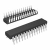
MAX135CPI
Analog Devices Inc./Maxim Integrated
IC ADC 15BIT MULTI-SLOPE 28DIP
CPH5870-TL-E
onsemi
NCH+SBD 2.5V DRIVE SERIES -

06035A6R2CAT4A
KYOCERA AVX
CAP CER 6.2PF 50V C0G/NP0 0603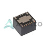
TPSM53604RDAR
FRESH DIGIT
Non-Isolated PoL Module
GRM1885C2AR80BA01D
Murata Electronics
CAP CER 0.8PF 100V C0G/NP0 0603
615008138221
Würth Elektronik
CONN MOD JACK 8P8C VERT SHIELDED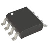
SI4384DY-T1-GE3
Vishay Siliconix
MOSFET N-CH 30V 10A 8SO
LTC1417ACGN#PBF
Analog Devices Inc.
IC ADC 14BIT SAR 16SSOP
UDZSTE-175.1B
Rohm Semiconductor
DIODE ZENER 5.1V 200MW UMD2
AZ1117R-3.3TRE1
Diodes Incorporated
IC REG LINEAR 3.3V 1.25A SOT89
FDP12N60NZ
onsemi
MOSFET N-CH 600V 12A TO220-3
80HCPS1432CHMGI
Renesas Electronics America Inc
IC SER RAPIDIO SWITCH 576FCBGA
LTC4085EDE-1#TRPBF
Analog Devices Inc.
IC BATT CHG LI-ION 1CELL 14DFN
08051C821KAT4A
KYOCERA AVX
CAP CER 820PF 100V X7R 0805
LT6654BHS6-2.5#TRPBF
Analog Devices Inc.
IC VREF SERIES 0.1% TSOT23-6
MM5Z4V7B
Diotec Semiconductor
ZENER, SOD-523, 4.7V, 0.3W, 2%
EKZM350ELL102MK20S
United Chemi-Con
CAP ALUM 1000UF 20% 35V RADIAL
TOP234YN
Power Integrations
IC OFFLINE SW FLYBACK TO220-7B
LP2980IM5X-ADJ
Texas Instruments
IC REG LIN POS ADJ 50MA SOT23-5
SA5534AD
onsemi
IC OPAMP GP 1 CIRCUIT 8SOIC