S9013 Transistor Explained: Pinout, Technical Specs, and Applications
NPN transistors, characterized by a P-type layer sandwiched between two N-type regions, play an active role in modern electronics by efficiently amplifying weak base signals into powerful collector outputs. Among these, the S9013 transistor stands out for its exceptional electron mobility and versatile functionality. Widely employed in audio systems, communication devices, and high-frequency circuits, the S9013 offers a unique blend of performance and adaptability. This article digs into the technical features, pin configuration, and practical applications of the S9013 transistor. From its structural design to its role in circuits like 12V switching regulators, we explore its capabilities, limitations, and use cases. This guide provides valuable insights into the S9013's role in driving innovation across various sectors.Catalog

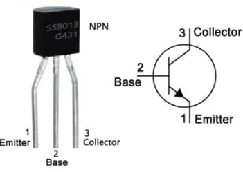
SS9013 Transistor Overview
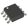
The S9013 transistor stands out with its remarkable capability for both high-speed and high-current operations, all encapsulated within the compact TO-92 package. This silicon epitaxial planar NPN transistor excels in both amplification and switching requirements across a broad range of commercial electronic applications. Featuring a composition of two N-doped layers encompassing a P-doped layer, this architecture is crafted with precision to enhance electron mobility, thereby facilitating effective current conduction. These attributes render the SS9013 mostly apt for roles such as audio output stages, inverters, and converters, emphasizing its broad applicability.
Possessing a DC gain of up to 150 and an operational frequency reaching as high as 140MHz, the SS9013 achieves commendable performance standards. It can support a collector current of up to 500mA and manage a power dissipation of up to 625mW. During practical use, it maintains stability across a spectrum of conditions, demonstrating reliability, mostly in circuitry demanding sustained, consistent performance over time.
Pin Configuration
|
Pin Number |
Pin Name |
Description |
|
Pin 1 |
Emitter |
Current supplies out of this emitter terminal |
|
Pin 2 |
Base |
The flow of current through this terminal controls the
current supply between the emitter & collector terminals. |
|
Pin 3 |
Collector |
Current flows throughout this terminal |
Features and Specs
|
Feature/Specification |
Details |
|
Transistor Type |
NPN |
|
Number of Terminals |
3 |
|
Package Type |
TO-92 |
|
Power Dissipation |
650 mW |
|
Maximum Collector Current (IC max) |
5 A / 500 mA |
|
Collector-to-Emitter Voltage (VCE) |
20 V |
|
Collector-to-Base Voltage (VCB) |
40 V |
|
Emitter-to-Base Voltage (VBE) |
5 V |
|
Maximum Collector Dissipation (Pc) |
625 mW |
|
Transition Frequency (fT) |
150 MHz |
|
DC Current Gain (hFE) Min & Max |
64 to 202 |
|
Gain Range |
40 (Min) to 300 (Max) |
|
Complementary PNP Transistor |
SS9012 |
|
Storage & Operating Temperature |
-55°C to +150°C |
|
Alternative/Equivalent Transistors |
S9013, 2N4401, S8050, 2N3904, BC547, BC338, BC337,
2N2222 |
Developing an Effective 12V Switching DC Regulator Circuit with Transistors
In modern power supply designs, integrated circuits are prized for their efficiency. This approach, however, leverages a pair of transistors aligned with essential components to transform a 15V-20V input into a steady 12V output. The circuit features transistors Q1-BD140 and Q2-S9013, utilizing elements such as the D1-1N5819 Schottky diode for rectification, a Zener diode (ZD1) for voltage regulation, capacitors (C1, C2, C3) for filtering, resistors (R1, R2, R3, R4, R5) for biasing and limiting, and the inductance L1 for energy storage. Careful assembly by the schematic diagram ensures precise current modulation and consistent output voltage, a testament to its versatility across various applications.

Circuit Functionality
Q1-BD140 acts as the main switch, collaborating closely with L1 and D1. The circuit's design includes both NPN and PNP transistors to enact a feedback loop for frequency control. A sophisticated voltage monitoring system through R4 and C2, along with support from Zener diode ZD1, preserves the output at 12V even when input levels waver. Upon receiving DC input, Q2-S9013 becomes active through R5, indirectly modulating Q1’s conductivity. Current guided through Q1’s emitter to the base is directed to L1, with Q2 overseeing the process, influenced by the regulated voltage of ZD1. When output exceeds 12V, Q2 turns off, stopping the current flowing through Q1, highlighting An actual need for consistent performance under fluctuating circumstances.
Optimizing Circuit Longevity
For sustained efficiency and safety, several practical measures should be observed. These involve capping the S9013 transistor’s operating voltage below 20V, incorporating a suitable current-limiting resistor, and ensuring precise pin alignments. Furthermore, keeping load connections below 500mA and operating temperatures between -55 and +150 degrees Celsius is advised to ensure enduring reliability. Such precautions are evaluated through continuous testing and iteration, signifying a blend of notional knowledge and practical experience in striving for long-term operability.
Pros and Cons
Pros
The S9013 transistor exhibits minimal power consumption, making it an attractive candidate for low-voltage endeavors. It is prominently featured in diverse applications due to its commendable energy management capabilities. The transistor boasts impressive DC gain and requires only an inconsequential base current to manipulate sizable collector currents, thus optimizing energy utilization. Additionally, its low saturation voltage between the collector and emitter contributes to enhanced energy efficiency. Its compact structure is valuable in environments where maximizing space is prioritized. You can appreciate its affordability and the economic solutions it brings to cost-sensitive projects, allowing for innovation without straining financial resources. In practical scenarios, you can often gravitate toward components that promise reliability and reduced energy consumption. These attributes contribute to extended device lifespans and reduced operational expenses.
Cons
The S9013 is not without its limitations, as it struggles with restricted power and voltage handling abilities and a limited frequency response range. These constraints can limit its effectiveness in high-power or broadband frequency applications, necessitating a strategic selection of components based on the intended project requirements. Being a polarized device, it demands accuracy in terminal connections; improper wiring can result in immediate operational issues or gradual degradation over time. This aspect requires careful consideration during installation and frequently calls for expertise. Insights from experience reveal that minor errors in wiring can lead to substantial system failures, emphasizing the importance of precise assembly processes and comprehensive testing to preserve device integrity and function.
Uses of the S9013 Transistor
The S9013 transistor holds a distinct position in electronics due to its versatility, originating from a 20V collector-emitter voltage rating. This moderate voltage characteristic contributes to its reliability across a wide range of practical applications.
Audio and Communication Devices
The S9013 is tailored for audio amplification tasks, catering specifically to low-power demands. It is extensively integrated into personal devices, including radios, alarms, and communication receivers. Delivering consistent audio fidelity, enriches your engagement, garnering appreciation from you who focus on intricate audio circuits.
Electronic Systems
Possessing a 500mA collector current capability, the S9013 excels in driving relays and integrated circuits (ICs). This current-handling prowess accommodates high-power LEDs and various switching processes, making the transistor a key element in circuits that demand reliability. Its adeptness at functioning in high-current scenarios aids in constructing electronic systems that respond quickly and dynamically.
Circuit Element
Beyond its roles in audio and driving tasks, the S9013 adeptly functions as a switch, amplifier, or rectifier within high-frequency circuits. This flexibility is valuable in intricate circuit designs, where components must adaptively perform varied roles. You can regularly count on its multi-functional characteristics to craft and implement innovative solutions in electronic design, ensuring both performance and dependability.
About us
ALLELCO LIMITED
Read more
Quick inquiry
Please send an inquiry, we will respond immediately.
Everything About PIC16F84A Microcontroller
on December 16th

Comprehensive Guide to SS34 Schottky Diode: Pinout, Specifications, Circuit Details, and Uses
on December 16th
Popular Posts
-

Complex Instruction Set Computers: How They Changed Computing?
on April 18th 147753
-

USB-C Pinout and Features
on April 18th 111927
-

Using Xilinx Unified Simulation Primitives: A Comprehensive Guide to FPGA Design and Simulation
on April 18th 111349
-

Power Supply Voltages in Electronics: Meaning of VCC, VDD, VEE, VSS, and GND
on April 18th 83714
-

RJ45 Connector Guide: Pinout, Wiring, Cable Types, and Uses
on January 1th 79504
-

The Ultimate Guide to Wire Color Codes in Modern Electrical Systems
The way our electrical systems use colors isn’t just for looks. Each wire color now indicates a specific function, making it easier to identify and handle electrical components correctly during ins...on January 1th 66872
-

Quality (Q) Factor: Equations and Applications
The quality factor, or 'Q', is important when checking how well inductors and resonators work in electronic systems that use radio frequencies (RF). 'Q' measures how well a circuit minimizes energy...on January 1th 63005
-

Purge Valve Guide: Function, Symptoms, Testing, and Replacement for Optimal Engine Performance
The purge valve is a key part of a car’s system that helps keep the air clean by managing fuel vapors before they can escape into the atmosphere. This not only helps the environment by reducing pol...on January 1th 62957
-

Achieving Peak Performance with the Maximum Power Transfer Theorem
The Maximum Power Transfer Theorem explains how energy from a source, such as a battery or generator, flows to a connected load. It shows the exact condition where the load receives the most power....on January 1th 54079
-

A23 Battery Specifications and Compatibility
The A23 battery is a small, cylinder-shaped battery with high voltage. Also called 23A, 23AE, or MN21, it runs at 12 volts and much higher than AA or AAA batteries. Its special design make...on January 1th 52093
HOT Part Number
-

RMPA0959
onsemi
IC RF AMP CELL 824-849MHZ 11LCC
RCLAMP0554S.TCT
Semtech Corporation
TVS DIODE 5VWM 15VC SOT23-6
CM453232-R47KL
Bourns Inc.
FIXED IND 470NH 545MA 320MOHM SM
744028002
Würth Elektronik
FIXED IND 2.2UH 1.3A 155MOHM SMD
MIC3809YMM
Microchip Technology
IC REG CTRLR MULT TOPOLOGY 8MSOP
AONS36302
Alpha & Omega Semiconductor Inc.
MOSFET N-CH 30V 146A 8DFN
SP3238EEA-L/TR
MaxLinear, Inc.
IC TRANSCEIVER FULL 5/3 28SSOP
BF5020WH6327
Infineon Technologies
N-CHANNEL POWER MOSFET
C1608X8R1H102M080AE
TDK Corporation
CAP CER 1000PF 50V X8R 0603
TPS71525QDCKRQ1
Texas Instruments
IC REG LINEAR 2.5V 50MA SC70-5
170M5444
Eaton - Bussmann Electrical Division
FUSE SQUARE 500A 1.3KVAC RECT
IHLP4040DZER220M1A
Vishay Dale
IHLP-4040DZ-1A 22 20% ER E3
C0603X181J1HACAUTO
KEMET
CAP CER 0603 180PF 100V ULTRA ST
PIC16F1575-E/JQ
Microchip Technology
IC MCU 8BIT 14KB FLASH 16UQFN
OPA4354AIPWR
Texas Instruments
IC CMOS 4 CIRCUIT 14TSSOP
P6SMB33A
Bourns Inc.
TVS DIODE 28.2VWM 45.7VC DO214AA
GCM1885C1H4R4CA16D
Murata Electronics
CAP CER 4.4PF 50V C0G/NP0 0603
R5F100LGAFB#10
Renesas Electronics America Inc
IC MCU 16BIT 128KB FLASH 64LFQFP -
TC621CCOA
Microchip Technology
THERMOSTAT PROG ACTIVE LOW 8SOIC
IRG4BC20UDPBF
International Rectifier
IGBT, 13A I(C), 600V V(BR)CES, N
MICROSMD175F-2
Littelfuse Inc.
PTC RESET FUSE 6V 1.75A 1210
AC0603KRX7R8BB222
YAGEO
CAP CER 2200PF 25V X7R 0603
1812AA150JAT1A\SB
KYOCERA AVX
CAP CER 15PF 1KV NP0 1812
SY10ELT22ZC
Microchip Technology
IC TRANSLTR UNIDIRECTIONAL 8SOIC
SCW03B-12
MEAN WELL USA Inc.
DC DC CONVERTER 12V 3W
A4840
Sensata-Crydom
SSR RELAY SPST-NO 40A 80-530V
TC4426AEOA
Microchip Technology
IC GATE DRVR LOW-SIDE 8SOIC
C1608NP01H470J080AA
TDK Corporation
CAP CER 47PF 50V NP0 0603
GRM1555C2A8R1DA01J
Murata Electronics
CAP CER 8.1PF 100V C0G/NP0 0402
INA330AIDGST
Texas Instruments
IC OPAMP GP 1 CIRCUIT 10VSSOP
12061C273KAT2A
KYOCERA AVX
CAP CER 0.027UF 100V X7R 1206
74LX1G70CTR
STMicroelectronics
IC BUF NON-INVERT 5.5V SOT323-5
CSNE151-204
Honeywell Sensing and Productivity Solutions
SENSOR CURRENT HALL 90A AC/DC
LF353DT
STMicroelectronics
IC OPAMP JFET 2 CIRCUIT 8SOIC
SMK316B7223KLHT
Taiyo Yuden
CAP CER 0.022UF 630V X7R 1206
R9G01612XX
Powerex Inc.
DIODE GP 1.6KV 1200A DO200AB -
FPF2300MPX
Fairchild Semiconductor
DUAL OUTPUT CURRENT LIMIT SWITCH
HZB6.8MWATL-E
Renesas Electronics America Inc
TVS DIODE 3.5VWM 3CMPAK
P0111MA 1AA3
STMicroelectronics
SCR 600V 800MA TO92-3
88E1545-A1-LKJ2C000
Marvell Semiconductor, Inc.
IC TXRX FULL/HALF 4/4 128LQFP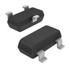
MAX809SN293D1T1G
onsemi
IC SUPERVISOR 1 CHANNEL SOT23-3
ICL3232IBZ-T
Renesas Electronics America Inc
IC TRANSCEIVER FULL 2/2 16SOIC
EP1K50FI484-2
Altera
LOADABLE PLD, 0.4NS PBGA484
FDMF6824C
onsemi
IC HALF BRIDGE DRIVER 50A 40PQFN
HVD144AKRF-E
Renesas Electronics America Inc
PLANAR PIN DIODE
MCD56-12IO1B
IXYS
MOD THYRISTOR/DIO 1200V TO-240AA
CD3275A0DRCR
Texas Instruments
PROTOTYPE
SN74ALS240ANSR
Texas Instruments
IC BUFFER INVERT 5.5V 20SO
9FG104EGLF
Renesas Electronics America Inc
IC FREQ TIMING GENERATOR 28TSSOP
MPC8548EVTAUJB
Freescale Semiconductor
MPU, 32-BIT, 1333MHZ, PBGA783
NCP1070STCT3G
onsemi
IC OFFLINE SWITCH FLYBACK SOT223
MIC4422YM
Microchip Technology
IC GATE DRVR LOW-SIDE 8SOIC
BU2510-E3/51
Vishay General Semiconductor - Diodes Division
BRIDGE RECT 1P 1KV 3.5A BU
GS8642Z36GB-167IV
GSI Technology Inc.
IC SRAM 72MBIT PARALLEL 119FPBGA