Understanding AD9959 Features for Signal Processing
The AD9959 is a powerful and flexible digital synthesizer that offers control over frequency, phase, and amplitude on four independent channels. This article covers the key features, technical specifications, and common applications of the AD9959, making it easier for you to understand how this device can be used in various setups. Whether you're looking to create agile local oscillators or synchronize complex systems like phased array radars, the AD9959 provides the precision and adaptability needed for a wide range of projects. By the end of this guide, you'll have a clear understanding of how the AD9959 works and how it can be applied in different fields.Catalog

Overview of AD9959
The AD9959 offers four direct digital synthesizer cores, allowing you to control frequency, phase, and amplitude independently for each channel. With the ability to handle up to 16 levels of modulation, whether it's frequency, phase, or amplitude, it brings flexibility to your designs. Since all channels share the same system clock, they stay synchronized, ensuring smooth operation across multiple channels. Moreover, if you're working with more than one AD9959, you can easily synchronize several devices, making it ideal for complex setups.
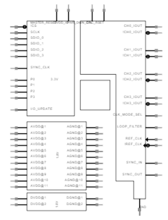
AD9959 Pinout Diagram

| Pin No. | Mnemonic | I/O | Description |
| 1 | SYNC_IN | I | Used to Synchronize Multiple AD9959 Devices. Connects to the SYNC_OUT pin of the master AD9959 device. |
| 2 | SYNC_OUT | O | Used to Synchronize Multiple AD9959 Devices. Connects to the SYNC_IN pin of the slave AD9959 device. |
| 3 | MASTER_RESET | I | Active High Reset Pin. Asserting the MASTER_RESET pin forces the AD9959 internal registers to their default state. |
| 4 | PWR_DWN_CTL | I | External Power-Down Control. |
| 5, 7, 11, 15, 19, 21, 26, 31, 33, 37, 39 | AVDD | I | Analog Power Supply Pins (1.8V). |
| 6, 10, 12, 16, 18, 20, 25, 28, 32, 34, 38 | AGND | I | Analog Ground Pins. |
| 44, 56 | DVDD | I | Digital Power Supply Pins (1.8V). |
| 45, 55 | DGND | I | Digital Power Ground Pins. |
| 8 | CH2_IOUT | O | True DAC Output. Terminates into AVDD. |
| 9 | CH2_IOUT | O | Complementary DAC Output. Terminates into AVDD. |
| 13 | CH3_IOUT | O | True DAC Output. Terminates into AVDD. |
| 14 | CH3_IOUT | O | Complementary DAC Output. Terminates into AVDD. |
| 17 | DAC_RSET | I | Establishes the Reference Current for All DACs. A 1.91 kΩ resistor (nominal) is connected from Pin 17 to AGND. |
| 22 | REF_CLK | I | Complementary Reference Clock/Oscillator Input. When the REF_CLK is operated in single-ended mode, this pin should be decoupled to AVDD or AGND with a 0.1 µF capacitor. |
| 23 | REF_CLK | I | Reference Clock/Oscillator Input. When the REF_CLK is operated in single-ended mode, this is the input. See the Modes of Operation section for the reference clock configuration. |
| Pin No. | Mnemonic | I/O | Description |
| 24 | CLK_MODE_SEL | I | Control Pin for the Oscillator Section. Caution: Do not drive this pin beyond 1.8V. When high (1.8V), the oscillator section is enabled to accept a crystal as the REF_CLK source. When low, the oscillator section is bypassed. |
| 27 | LOOP_FILTER | I | Connects to the external zero compensation network of the PLL loop filter. Typically, the network consists of a 0Ω resistor in series with a 680pF capacitor tied to AVDD. |
| 29 | CH0_IOUT | O | Complementary DAC Output. Terminates into AVDD. |
| 30 | CH0_IOUT | O | True DAC Output. Terminates into AVDD. |
| 35 | CH1_IOUT | O | Complementary DAC Output. Terminates into AVDD. |
| 36 | CH1_IOUT | O | True DAC Output. Terminates into AVDD. |
| 40 to 43 | P0 to P3 | I | Data pins used for modulation (FSK, PSK, ASK), to start/stop the sweep accumulators or used to ramp up/ramp down the output amplitude. The data is synchronous to the SYNC_CLK (Pin 54). Data inputs must meet the setup and hold time requirements of SYNC_CLK. The functionality of these pins is controlled by the profile pin configuration (PPC) bits (FR1[14:12]). |
| 46 | I/O_UPDATE | I | A rising edge transfers data from the serial I/O port buffer to active registers. I/O_UPDATE is synchronous to the SYNC_CLK (Pin 54). I/O_UPDATE must meet the setup and hold time requirements of SYNC_CLK to guarantee a fixed pipeline delay of data to the DAC output; otherwise, ±1 SYNC_CLK period of pipeline uncertainty exists. The minimum pulse width is one SYNC_CLK period. |
| 47 | CS\ | I | Active Low Chip Select. Allows multiple devices to share a common I/O bus (SPI). |
| 48 | SCLK | I | Serial Data Clock for I/O operations. Data bits are written on the rising edge of SCLK and read on the falling edge of SCLK. |
| 49 | DVDD_I/O | I | 3.3V Digital Power Supply for SPI Port and Digital I/O. |
| 50 | SDIO_0 | I/O | Data Pin SDIO_0 is dedicated to the serial port I/O only. |
| 51, 52 | SDIO_1, SDIO_2 | I/O | Data Pin SDIO_1 and Data Pin SDIO_2 can be used for the serial I/O port or used to initiate a ramp-up/ramp-down (RU/RD) of the DAC Output amplitude. |
| 53 | SDIO_3 | I/O | Data Pin SDIO_3 can be used for the serial I/O port or to initiate a ramp-up/ramp-down (RU/RD) of the DAC output amplitude. In single-bit or 2-bit modes, SDIO_3 is used for SYNC_I/O. If the SYNC_I/O function is not used, tie it to ground or logic 0. Do not let SDIO_3 float in single-bit or 2-bit modes. |
| 54 | SYNC_CLK | O | The SYNC_CLK runs at one-fourth the system clock rate; it can be disabled. I/O_UPDATE or data (Pin 40 to Pin 43) is synchronous to SYNC_CLK. To guarantee a fixed pipeline delay of data to DAC output, I/O_UPDATE or data (Pin 40 to Pin 43) must meet the setup and hold time requirements to the rising edge of SYNC_CLK; otherwise, ±1 SYNC_CLK period of uncertainty occurs. |
AD9959 CAD Model Overview
AD9959 Symbol
AD9959 Footprint

Detailed AD9959 Block Diagram

AD9959 Technical Specifications
Technical specifications, attributes, parameters, and comparable parts for the Analog Devices Inc. AD9959BCPZ.
| Type | Parameter |
| Lifecycle Status | |
| Factory Lead Time | 8 Weeks |
| Contact Plating | Tin |
| Mount | Surface Mount |
| Mounting Type | Surface Mount |
| Package / Case | 56-VFQFN Exposed Pad, CSP |
| Number of Pins | 56 |
| Operating Temperature | -40°C to 85°C |
| Packaging | Tray |
| JESD-609 Code | e3 |
| Pbfree Code | No |
| Part Status | Active |
| Moisture Sensitivity Level (MSL) | 3 (168 Hours) |
| Number of Terminations | 56 |
| Termination | SMD/SMT |
| ECCN Code | EAR99 |
| Additional Feature | Also Requires 3.3V Supply |
| Max Power Dissipation | 680mW |
| Voltage - Supply | 1.71V to 1.96V |
| Terminal Position | QUAD |
| Terminal Form | No Lead |
| Peak Reflow Temperature (°C) | 260 |
| Supply Voltage | 1.8V |
| Terminal Pitch | 0.5mm |
| Frequency | 500MHz |
| Time @ Peak Reflow Temp (s) | 30 |
| Base Part Number | AD9959 |
| Pin Count | 56 |
| Qualification Status | Not Qualified |
| Operating Supply Voltage | 1.8V |
| Interface | Serial |
| Operating Supply Current | 180mA |
| Nominal Supply Current | 160mA |
| Max Supply Current | 185mA |
| uPs/uCs/Peripheral ICs Type | |
| Number of Bits | 10 |
| Sampling Rate | 500 Msps |
| Boundary Scan | No |
| Low Power Mode | Yes |
| Conversion Rate | 500 Msps |
| Number of D/A Converters | 4 |
| Resolution (Bits) | 10 b |
| Tuning Word Width (Bits) | 32 b |
| Height | 830μm |
| Length | 8mm |
| Width | 8mm |
| REACH SVHC | No SVHC |
| RoHS Status | ROHS3 Compliant |
| Lead Free | Contains Lead |
AD9959 Key Features
4 Synchronized DDS Channels at 500 MSPS
The AD9959 provides four synchronized direct digital synthesizer (DDS) channels, all operating at up to 500 MSPS. This lets you generate precise signals across multiple channels while maintaining synchronization, which is especially useful when working on projects requiring multiple outputs working together smoothly.
Independent Frequency, Phase, and Amplitude Control
Each of the four DDS channels offers independent control over frequency, phase, and amplitude. This allows you to fine-tune each channel to suit different needs, giving you flexibility in handling various signal parameters.
Matched Latencies for Frequency, Phase, and Amplitude Changes
The AD9959 ensures that changes in frequency, phase, and amplitude are synchronized across channels. This means when you adjust one parameter, the change happens simultaneously on all channels, helping you maintain consistent outputs without lag.
Excellent Channel-to-Channel Isolation
With over 65 dB of channel-to-channel isolation, the AD9959 minimizes interference between channels. This ensures that the signals generated on each channel are clean and distinct, providing a higher quality performance in your designs.
Linear Sweeping Capability
The AD9959 supports linear frequency, phase, and amplitude sweeping. This feature allows you to smoothly transition between values, making it easier to generate signals that gradually change over time, which can be useful for testing and calibration purposes.
Up to 16 Levels of Frequency, Phase, and Amplitude Modulation
The device can handle up to 16 levels of modulation for frequency, phase, or amplitude. This level of flexibility enables you to implement a variety of modulation schemes, from simple to complex, depending on your project needs.
Integrated 10-bit Digital-to-Analog Converters (DACs)
Each channel comes with its own integrated 10-bit DAC, allowing you to convert digital signals into analog outputs with precision. This makes the AD9959 a great choice when you need accurate analog signal generation in a compact form.
Individually Programmable DAC Full-Scale Currents
You can program the full-scale current for each DAC individually, which gives you control over the output power of each channel. This level of customization allows you to optimize the power level for different channels based on your specific requirements.
Fine Frequency Tuning Resolution
The AD9959 offers a tuning resolution of 0.12 Hz or better, providing precise control over the frequency of the signals you generate. This level of accuracy is beneficial when working on applications where small frequency adjustments make a big difference.
High-Resolution Phase Offset
With 14-bit phase offset resolution, the AD9959 lets you fine-tune the phase of each channel. This feature is helpful when you need exact phase adjustments between signals, such as when aligning multiple signals in phased-array systems.
Output Amplitude Scaling
The AD9959 provides 10-bit output amplitude scaling resolution. This allows you to adjust the output amplitude with high precision, giving you the flexibility to control the signal strength more accurately.
Enhanced Serial I/O Port Interface
The serial I/O port interface (SPI) offers enhanced data throughput, allowing you to transfer data quickly and efficiently between the device and your system. This speeds up communication, which can be useful in fast-paced applications.
Power-Down Control
The AD9959 includes both software and hardware options for powering down, giving you control over how and when to save power. This feature is particularly useful in energy-conscious designs where power efficiency is a priority.
Dual Supply Operation
The device operates with a dual supply system: 1.8 V for the DDS core and 3.3 V for the serial I/O. This configuration helps balance performance with power needs, making it adaptable to various design environments.
Multiple Device Synchronization
The AD9959 supports synchronization across multiple devices, allowing you to expand your design with additional units while maintaining precise timing between them. This makes it easier to scale your projects without losing synchronization.
Selectable REFCLK Multiplier
With a selectable REFCLK multiplier ranging from 4× to 20×, the AD9959 offers flexibility in clocking options, allowing you to choose the best setting for your design.
Built-in REFCLK Crystal Oscillator
The device includes a built-in REFCLK crystal oscillator, which simplifies your design process by reducing the need for external components, making it easier to manage timing within the system.
Compact 56-lead LFCSP Package
The AD9959 comes in a 56-lead LFCSP package, providing a compact and space-saving option for integrating multiple DDS channels into your design. This small form factor is ideal when you need high functionality without taking up too much board space.
Common AD9959 Applications
Agile Local Oscillators
The AD9959 is well-suited for use in agile local oscillators, providing precise control over frequency, phase, and amplitude. This makes it a great option when you need flexible and adjustable signal generation in radio systems or other communications equipment.
Phased Array Radars and Sonars
In phased array radar and sonar systems, precise synchronization of multiple signal channels is critical. The AD9959’s ability to handle independent control and synchronization across multiple channels makes it a perfect fit for these applications, ensuring accurate signal processing and timing.
Instrumentation
The AD9959 can be used in various types of instrumentation, particularly in devices that require precise signal generation and control. Whether it's for testing, measuring, or calibrating systems, the device's flexibility in adjusting frequency, phase, and amplitude adds versatility to your designs.
Synchronized Clocking
For projects that need synchronized clocking across multiple channels, the AD9959 offers an excellent solution. Its built-in synchronization features allow you to maintain exact timing between channels, making it ideal for systems where timing accuracy is crucial.
RF Source for Acousto-Optic Tunable Filters (AOTF)
The AD9959 can act as an RF source for Acousto-Optic Tunable Filters (AOTF), providing reliable and precise signal generation for these optical systems. Its flexibility in frequency and amplitude control allows it to meet the demands of such specialized applications.
AD9959 Application Circuit Overview

AD9959 Dimension Outline Diagram

AD9959 Manufacturer Information
Analog Devices has been a leading company in creating integrated circuits since 1965. The company specializes in designing and producing circuits that help convert, condition, and process signals from the real world—like temperature, sound, and motion—into electrical signals. These circuits are used in a wide range of electronic systems across the globe.
Frequently Asked Questions [FAQ]
1. What is the AD9959 used for?
The AD9959 contains four direct digital synthesizer (DDS) cores, each allowing independent control of frequency, phase, and amplitude on its respective channel. This flexibility can help you balance out any inconsistencies in signals caused by analog processes like filtering, amplification, or layout differences on the PCB.
2. How does the AD9959 work?
The AD9959 can modulate frequency, phase, or amplitude (using FSK, PSK, or ASK modulation) with up to 16 distinct levels. You control this modulation by applying signals to the profile pins, which allows the chip to switch between different modulation levels as needed.
About us
ALLELCO LIMITED
Read more
Quick inquiry
Please send an inquiry, we will respond immediately.

A Comprehensive Guide to the TC7660COA Voltage Converter
on October 24th

Understanding TIP120 Transistor
on October 24th
Popular Posts
-

Complex Instruction Set Computers: How They Changed Computing?
on April 18th 147751
-

USB-C Pinout and Features
on April 18th 111923
-

Using Xilinx Unified Simulation Primitives: A Comprehensive Guide to FPGA Design and Simulation
on April 18th 111349
-

Power Supply Voltages in Electronics: Meaning of VCC, VDD, VEE, VSS, and GND
on April 18th 83714
-

RJ45 Connector Guide: Pinout, Wiring, Cable Types, and Uses
on January 1th 79502
-

The Ultimate Guide to Wire Color Codes in Modern Electrical Systems
The way our electrical systems use colors isn’t just for looks. Each wire color now indicates a specific function, making it easier to identify and handle electrical components correctly during ins...on January 1th 66872
-

Quality (Q) Factor: Equations and Applications
The quality factor, or 'Q', is important when checking how well inductors and resonators work in electronic systems that use radio frequencies (RF). 'Q' measures how well a circuit minimizes energy...on January 1th 63005
-

Purge Valve Guide: Function, Symptoms, Testing, and Replacement for Optimal Engine Performance
The purge valve is a key part of a car’s system that helps keep the air clean by managing fuel vapors before they can escape into the atmosphere. This not only helps the environment by reducing pol...on January 1th 62955
-

Achieving Peak Performance with the Maximum Power Transfer Theorem
The Maximum Power Transfer Theorem explains how energy from a source, such as a battery or generator, flows to a connected load. It shows the exact condition where the load receives the most power....on January 1th 54078
-

A23 Battery Specifications and Compatibility
The A23 battery is a small, cylinder-shaped battery with high voltage. Also called 23A, 23AE, or MN21, it runs at 12 volts and much higher than AA or AAA batteries. Its special design make...on January 1th 52092
HOT Part Number
-

AP2553FDC-7
Diodes Incorporated
IC PWR SWITCH P-CHANNEL 1:1 6DFN
REG1117FA-5.0/500
Texas Instruments
IC REG LIN 5V 1A DDPAK/TO263-3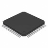
DSPIC33CH64MP508-I/PT
Microchip Technology
IC MCU 16BIT 88KB FLASH 80TQFP
NVTFS5826NLWFTWG
onsemi
MOSFET N-CH 60V 7.6A 8WDFN
CL03C180JA3ANNC
Samsung Electro-Mechanics
CAP CER 18PF 25V C0G/NP0 0201
C1608X8R1H103M080AE
TDK Corporation
CAP CER 10000PF 50V X8R 0603
LTC1682IMS8-5#PBF
Analog Devices Inc.
IC REG CHARGE PUMP 5V 50MA 8MSOP
PXAS30KBA
Rochester Electronics, LLC
IC MCU 16BIT ROMLESS 68PLCC
C3216Y5V1C106Z
TDK Corporation
CAP CER 10UF 16V Y5V 1206
ADA4610-1ARZ-R7
Analog Devices Inc.
IC OPAMP JFET 1 CIRCUIT 8SOIC
BYM11-200-E3/97
Vishay General Semiconductor - Diodes Division
DIODE GEN PURP 200V 1A DO213AB
GRM2167U1H560JZ01D
Murata Electronics
CAP CER 56PF 50V U2J 0805
TOP258GN-TL
Power Integrations
IC OFFLINE SWITCH FLYBACK 8SMD
STM8S207RBT3
STMicroelectronics
IC MCU 8BIT 128KB FLASH 64LQFP
XC6701B502MR-G
Torex Semiconductor Ltd
IC REG LINEAR 5V 150MA SOT25
08053G104ZAT2A
AVX Corporation
CAP CER 0.1UF 25V Y5V 0805
BZM55B13-TR
Vishay General Semiconductor - Diodes Division
DIODE ZENER 13V 500MW MICROMELF
MCH5809-TL-E
onsemi
NCH+SBD 2.5V DRIVE SERIES -

BZD17C3V6P-E3-08
Vishay General Semiconductor - Diodes Division
DIODE ZENER 3.6V 800MW DO219AB
DSRHD06-13
Diodes Incorporated
BRIDGE RECT 1P 600V 1A T-MINIDIP
BCX54-16E6327
Infineon Technologies
SMALL SIGNAL BIPOLAR TRANSISTOR
AD9961BCPZ
Analog Devices Inc.
IC BROADBAND FRONT-END 72LFCSP
AT80C51RD2-RLRUM
Microchip Technology
IC MCU 8BIT ROMLESS 44VQFP
PHK31NQ03LT,518
Nexperia USA Inc.
MOSFET N-CH 30V 30.4A 8SO
1469002-1
TE Connectivity AMP Connectors
CONN HDR HIGH SPEED 120POS PCB
S5JHE3_A/I
Vishay General Semiconductor - Diodes Division
DIODE GEN PURP 600V 5A DO214AB
SCAN90004TVS
Texas Instruments
IC REDRIVER LVDS 4CH 48TQFP
CD4025BCN
onsemi
IC GATE NOR 3CH 3-INP 14DIP
2225HC332KAT1A
KYOCERA AVX
CAP CER 3300PF 3KV X7R 2225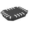
MN63Y1208-E1
Panasonic Electronic Components
IC RFID READR/TRAN 13.56MZ 16QFN
06035C112JAT2A
KYOCERA AVX
CAP CER 1100PF 50V X7R 0603
LFE3-95EA-8LFN672I
Lattice Semiconductor Corporation
IC FPGA 380 I/O 672FPBGA
XBS053V13R-G
Torex Semiconductor Ltd
DIODE SCHOTTKY 20V 500MA SOD323A
GRM0335C2A6R5CA01J
Murata Electronics
CAP CER 6.5PF 100V C0G/NP0 0201
STW36N55M5
STMicroelectronics
MOSFET N-CH 550V 33A TO247
C1608C0G2A090D080AA
TDK Corporation
CAP CER 9PF 100V C0G 0603 -
GRM1886P1H4R8CZ01D
Murata Electronics
CAP CER 4.8PF 50V P2H 0603
M29W128FL70N6E
Micron Technology Inc.
IC FLASH 128MBIT PARALLEL 56TSOP
70MT100KB
Vishay General Semiconductor - Diodes Division
BRIDGE RECT 3PHASE 1KV 70A MTK
ADXL344ACCZ-RL7
Analog Devices Inc.
ACCEL 2-16G I2C/SPI 16LGA
BZX84C39-HE3-08
Vishay General Semiconductor - Diodes Division
DIODE ZENER 39V 300MW SOT23-3
1735447-7
TE Connectivity AMP Connectors
CONN RCPT HSG 7POS 2.00MM
1808AA150JAT1A
KYOCERA AVX
CAP CER 15PF 1KV NP0 1808
Z84C4106PEC
Zilog
IC INTERFACE SPECIALIZED 40DIP
GRM1555C1H7R4WZ01D
Murata Electronics
CAP CER 7.4PF 50V C0G/NP0 0402
BDCN-20-13+
Mini-Circuits
RF DIR COUPLER 360MHZ-1GHZ 6SMD
MCC19-14IO1B
IXYS
MOD THYRISTOR DUAL 1400V TO240AA
OP467GPZ
Analog Devices Inc.
IC OPAMP GP 4 CIRCUIT 14DIP
LA4636-E
Sanyo
11 WATT 2-CHANNEL BTL AF POWER A
P6KE82A-T
Diodes Incorporated
TVS DIODE 70.1VWM 113VC DO15
NCV7608DWR2G
onsemi
IC HALF BRIDGE DRIVER 28SOIC
TLJA227M004R1100
KYOCERA AVX
CAP TANT 220UF 20% 4V 1206
TUSB2136PM
Texas Instruments
IC USB HUB I/O CONTROL 64-LQFP
HUFA75637P3
onsemi
MOSFET N-CH 100V 44A TO220-3