Understanding LFSC3GA25E-7F900C FPGA Architecture and Key Functions
Exploring the LFSC3GA25E-7F900C gives you a closer look at how programmable logic devices support flexible digital systems. You can use this FPGA to organize data paths, manage signals, and build custom logic functions inside a single chip. Its internal layout combines programmable logic cells, memory blocks, and input output banks so signals move efficiently through the device. Understanding how these sections work together helps you see how complex electronic systems are structured. From communication hardware to control systems, this FPGA offers a practical way to create adaptable digital designs.Catalog
LFSC3GA25E-7F900C Overview
LFSC3GA25E-7F900C is a programmable logic device designed to support configurable digital functions in embedded electronic systems. The device contains a grid based logic structure with thousands of programmable elements, internal memory resources, and numerous input and output connections for external communication. Its architecture allows digital circuits, control paths, and signal processing tasks to be implemented within a single chip. Integrated routing networks connect logic blocks and memory sections so data can move through the device in a structured way. Operation is supported by a low core supply range and a high pin count package suited for dense board layouts.
Looking for LFSC3GA25E-7F900C. Contact us to check current stock, lead time, and pricing.
Banks of LFSC3GA25E-7F900C
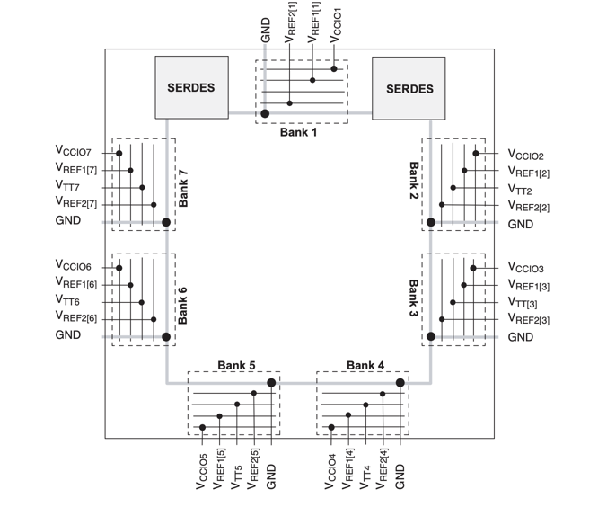
Input and output bank arrangement used in the LFSC3GA25E-7F900C FPGA showing how the device organizes its programmable I O resources into multiple voltage controlled regions. Eight banks are distributed around the device perimeter and each bank includes grouped connections for VCCIO supply, reference voltage inputs labeled VREF, termination voltage pins labeled VTT, and ground. This structure allows each bank to operate with independent electrical conditions so different signal standards can be supported on separate sides of the device. SERDES interface blocks appear near the upper banks to support high speed serial communication channels connected to nearby I O regions. The layout also identifies shared reference pins and power connections that define how external signals interact with the internal programmable logic through the banked I O structure.
LFSC3GA25E-7F900C CAD Model
LFSC3GA25E-7F900C Symbol
LFSC3GA25E-7F900C Footprint

LFSC3GA25E-7F900C 3D Model
Features of LFSC3GA25E-7F900C
High Density Programmable Logic
The device integrates around twenty five thousand programmable logic elements arranged in an organized grid. These logic cells can be configured to implement digital control paths, combinational logic, and arithmetic operations within embedded systems.
Embedded Memory Architecture
Internal memory resources provide more than one megabit of storage capacity for buffering data and supporting logic operations. These memory blocks are distributed throughout the device so logic circuits can access data locally without long routing paths.
Flexible Input And Output Connectivity
Up to three hundred seventy eight input and output connections allow the device to interact with sensors, communication interfaces, and other digital components. The pin structure supports multiple electrical standards across independent I O banks.
Integrated Clock Management Resources
Internal clock management blocks help distribute timing signals across the programmable logic structure. These resources maintain synchronized signal timing so digital operations occur in an orderly and predictable sequence.
High Speed Serial Interface Capability
Dedicated serial interface blocks support high speed communication channels for data transfer between system modules. These blocks connect to nearby I O banks and help maintain stable signal transmission in data intensive designs.
Structured Logic Processing Blocks
Specialized internal processing blocks extend the logic fabric and allow designers to implement repeated digital structures more efficiently. This arrangement supports tasks such as packet handling, control sequencing, and parallel data operations.
Programmable Routing Network
A structured routing network links logic cells, memory blocks, and interface pins. Signals can travel through the network along multiple paths, allowing designers to organize digital functions in ways that match the system architecture.
Surface Mount Package Integration
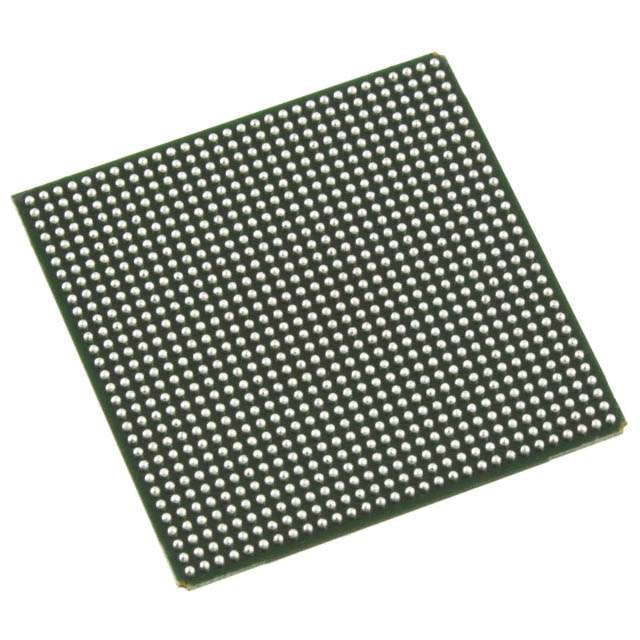
The device is housed in a large ball grid array package that supports dense board integration. This package structure allows many electrical connections to be arranged in a compact footprint for advanced electronic assemblies.
LFSC3GA25E-7F900C Technical Specifications
| Product Attribute | Attribute Value |
| Manufacturer | Lattice Semiconductor |
| Voltage - Supply | 0.95V ~ 1.26V |
| Total RAM Bits | 1966080 |
| Supplier Device Package | 900-FPBGA (31x31) |
| Series | SC |
| Package / Case | 900-BBGA |
| Package | Tray |
| Operating Temperature | 0°C ~ 85°C (TJ) |
| Number of Logic Elements/Cells | 25000 |
| Number of LABs/CLBs | 6250 |
| Number of I/O | 378 |
| Mounting Type | Surface Mount |
| Base Product Number | LFSC3GA25 |
| RoHS Status | RoHS non-compliant |
| Moisture Sensitivity Level (MSL) | 3 (168 Hours) |
| REACH Status | REACH Unaffected |
| ECCN | 3A991D |
| HTSUS | 8542.39.0001 |
Simplified Block Diagram of LFSC3GA25E-7F900C
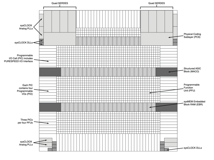
Grid based internal layout of the LFSC3GA25E-7F900C FPGA showing the arrangement of programmable logic, memory blocks, clock resources, and high speed interface structures. Programmable function units form the central logic fabric where configurable digital circuits are implemented. Distributed sysMEM embedded block RAM sections provide internal data storage and buffering within the logic array. Programmable I O cells positioned along the device edges connect internal logic to external pins, with each programmable I O cluster containing multiple programmable I O connections. Quad SERDES blocks and physical coding sublayer interfaces appear near the top regions to support high speed serial communication. Structured ASIC blocks labeled MACO are integrated within the logic fabric to support specialized processing structures. Clock management resources labeled sysCLOCK analog PLLs and sysCLOCK DLLs are placed at the edges of the layout to generate and distribute timing signals across the programmable architecture.
Slice Diagram of LFSC3GA25E-7F900C
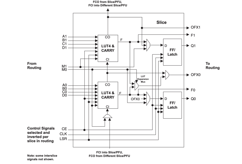
Internal structure of a logic slice used within the programmable function unit of the LFSC3GA25E-7F900C FPGA. Two LUT4 blocks perform combinational logic operations using four input signals labeled A, B, C, and D. Integrated carry logic supports arithmetic operations by linking carry input and carry output signals between adjacent slices. Flip flop or latch elements store output data from the logic stage, producing registered outputs labeled Q0 and Q1. Control inputs such as clock, clock enable, and set or reset signals regulate sequential operation of the storage elements. Routing connections on the left and right edges link the slice to the surrounding programmable interconnect network, allowing signals to enter from routing resources and return processed outputs back to the routing fabric.
Applications of LFSC3GA25E-7F900C
Industrial Control Systems
Programmable logic resources allow the device to manage timing sequences, signal routing, and digital control tasks in automated equipment. It can coordinate multiple sensors and actuators while maintaining stable digital processing within the control system.
Data Communication Infrastructure
Communication equipment often requires flexible digital processing for data handling and interface control. The device can process incoming data streams, organize routing logic, and support communication links within network hardware.
Embedded Computing Platforms
Embedded systems use programmable logic to manage data flow between processors, memory, and interface devices. The device can implement custom digital paths that adapt system behavior to specific application requirements.
High Speed Data Acquisition Systems
Measurement systems frequently collect signals from multiple sources at the same time. The programmable logic structure can organize incoming digital signals, align timing, and prepare the data for further processing or transfer.
Signal Processing Hardware
The device can implement configurable arithmetic and logical operations that support signal processing functions. Digital filters, control loops, and data transformation tasks can be implemented directly within the programmable logic structure.
LFSC3GA25E-7F900C Advantages and Disadvantages
Advantages
• Large programmable logic capacity supports complex digital functions
• High number of input and output connections allows flexible system integration
• Embedded memory blocks provide internal data storage and buffering
• Reconfigurable logic structure allows hardware functions to be updated through design changes
• Multiple I O banks allow different signal standards within one device
Disadvantages
• Design process requires specialized development tools and configuration workflows
• Device complexity may increase system design time during development
• Large package size requires careful printed circuit board layout
• Power management must be considered when many logic resources are active
LFSC3GA25E-7F900C Alternatives
| Part Number | Manufacturer | Key Features | Use Case/Notes |
| LFSC3GA25E-7FFN1020C | Lattice Semiconductor Corporation | FPGA device from the SC family offering about 25,000 logic elements, embedded memory resources, and a large number of programmable I/O pins. It uses a fine pitch BGA package that supports dense circuit layouts and complex digital designs. | Used in embedded control systems, communication interfaces, and industrial electronics where programmable hardware and high I/O connectivity are needed. |
| LFSC3GA25E-7FFA1020C | Lattice Semiconductor Corporation | Programmable FPGA with similar logic resources in the LFSC3GA25E series. Provides configurable logic blocks, embedded memory, and flexible digital routing that allow designers to implement custom digital circuits. | Suitable for digital signal processing, interface bridging, and programmable hardware control in embedded electronics and communication systems. |
| LFSC3GA25E-6FN900C | Lattice Semiconductor Corporation | FPGA device with around 25K logic elements and integrated memory blocks designed for programmable digital hardware. The package provides many I/O connections that support complex system integration. | Often used in industrial control systems, embedded computing platforms, and networking equipment that require flexible hardware configuration. |
About Lattice Semiconductor
Lattice Semiconductor is a semiconductor company founded in 1983 and headquartered in Hillsboro Oregon in the United States. The company develops programmable logic devices and related technologies used in computing, communications, industrial systems, and consumer electronics. Its product lines include field programmable gate arrays, programmable logic devices, and interface solutions designed to support flexible digital system design. Lattice devices are widely used in embedded systems where programmable hardware functions help manage data processing, control logic, and signal routing within compact electronic platforms.
Conclusion
The LFSC3GA25E-7F900C FPGA combines programmable logic, embedded memory, and flexible input output connections within a single device. By understanding its architecture, you can see how digital logic functions are organized and how signals travel across the programmable fabric. Features such as configurable logic elements, routing networks, and clock management blocks allow the device to support many system designs. Its structure makes it suitable for data processing, control logic, and communication hardware. When you explore the diagrams and specifications, you gain a clearer picture of how programmable hardware supports adaptable electronic systems.
Datasheet PDF
LFSC3GA25E-7F900C Datasheet:
All Dev Pkg Mark Chg 12/Nov/2018.pdf
About us
ALLELCO LIMITED
Read more
Quick inquiry
Please send an inquiry, we will respond immediately.
Frequently Asked Questions [FAQ]
1. What type of device is LFSC3GA25E-7F900C?
LFSC3GA25E-7F900C is a field programmable gate array, or FPGA, that allows digital logic circuits to be configured through hardware programming. It contains programmable logic blocks, routing resources, and memory elements inside a single chip.
2. What are logic elements in the LFSC3GA25E-7F900C FPGA?
Logic elements are small programmable units inside the FPGA that perform digital operations such as logical comparisons, arithmetic tasks, and signal processing. Thousands of these elements work together to create custom hardware functions.
3. How do I O banks work in this FPGA?
Input output banks group sets of pins that share power and reference voltages. Each bank can support different electrical standards, which allows signals from multiple interfaces to connect to the same device.
4. What is the purpose of embedded memory in the device?
Embedded memory blocks store data within the FPGA so logic circuits can access information quickly. These blocks are used for buffering data, temporary storage, and supporting signal processing tasks.
5. Where is LFSC3GA25E-7F900C typically used?
This FPGA is commonly used in communication systems, industrial control hardware, digital signal processing equipment, and embedded electronic platforms where programmable digital logic is needed.
What the EPF8282AVTC100-4 FPGA Does in Digital Systems
on March 10th

What Is an H7 Battery? Size, Features, and Vehicle Uses
on March 10th
Popular Posts
-

Complex Instruction Set Computers: How They Changed Computing?
on April 17th 147721
-

USB-C Pinout and Features
on April 17th 111788
-

Using Xilinx Unified Simulation Primitives: A Comprehensive Guide to FPGA Design and Simulation
on April 17th 111328
-

Power Supply Voltages in Electronics: Meaning of VCC, VDD, VEE, VSS, and GND
on April 17th 83652
-

RJ45 Connector Guide: Pinout, Wiring, Cable Types, and Uses
on January 1th 79369
-

The Ultimate Guide to Wire Color Codes in Modern Electrical Systems
The way our electrical systems use colors isn’t just for looks. Each wire color now indicates a specific function, making it easier to identify and handle electrical components correctly during ins...on January 1th 66808
-

Quality (Q) Factor: Equations and Applications
The quality factor, or 'Q', is important when checking how well inductors and resonators work in electronic systems that use radio frequencies (RF). 'Q' measures how well a circuit minimizes energy...on January 1th 62968
-

Purge Valve Guide: Function, Symptoms, Testing, and Replacement for Optimal Engine Performance
The purge valve is a key part of a car’s system that helps keep the air clean by managing fuel vapors before they can escape into the atmosphere. This not only helps the environment by reducing pol...on January 1th 62862
-

Achieving Peak Performance with the Maximum Power Transfer Theorem
The Maximum Power Transfer Theorem explains how energy from a source, such as a battery or generator, flows to a connected load. It shows the exact condition where the load receives the most power....on January 1th 54050
-

A23 Battery Specifications and Compatibility
The A23 battery is a small, cylinder-shaped battery with high voltage. Also called 23A, 23AE, or MN21, it runs at 12 volts and much higher than AA or AAA batteries. Its special design make...on January 1th 52032
HOT Part Number
-
TC426EPA
Microchip Technology
IC GATE DRVR LOW-SIDE 8DIP
PM5370-FGI
Microchip Technology
IC TELECOM INTERFACE 672FCBGA
RT0402DRD07147RL
YAGEO
RES SMD 147 OHM 0.5% 1/16W 0402
AK6514CF
Asahi Kasei Microdevices/AKM
IC EEPROM 128KBIT SPI 10MHZ 8SOP
MCP1653R-E/UN
Microchip Technology
IC REG CTRLR MULT TOP 10MSOP
CGA6M3X7T2E334K200AE
TDK Corporation
CAP CER 0.33UF 250V X7T 1210
9FGV0641AKLFT
Renesas Electronics America Inc
VFQFPN 5.00X5.00X0.90 MM, 0.40MM
BC848CWT1G
onsemi
TRANS NPN 30V 0.1A SC70-3
PE-52627NL
Pulse Electronics
FIXED IND 330UH 1A 780 MOHM TH
CD54AC00F3A
Texas Instruments
MILITARY 4-CH, 2-INPUT, 1.5-V TO
ADG1611BRUZ-REEL
Analog Devices Inc.
IC SW SPST-NCX4 1.1OHM 16TSSOP
SI32267-C-FM1R
Skyworks Solutions Inc.
IC TELECOM INTERFACE 50QFN
ATA5745C-PXQW-1
Microchip Technology
RF RECEIVER UHF 433MHZ 24VQFN
SN74CBTD3306PWRG4
Texas Instruments
IC BUS SWITCH 1 X 1:1 8TSSOP
MIC2920A-12BS
Microchip Technology
IC REG LINEAR 12V 400MA SOT223-3
PIC16LF1786-I/ML
Microchip Technology
IC MCU 8BIT 14KB FLASH 28QFN
KBP308G
Diodes Incorporated
BRIDGE RECTIFIER KBP TUBE 35PCS
GRM1555C1HR30BA01J
Murata Electronics
CAP CER 0.3PF 50V C0G/NP0 0402 -
SY89833ALMG-TR
Microchip Technology
IC CLK BUFFER 1:4 2GHZ 16MLF
170M7035
Eaton - Bussmann Electrical Division
FUSE SQUARE 2200A 1KV RECT
KSP44BU
Fairchild Semiconductor
SMALL SIGNAL BIPOLAR TRANSISTOR,
71M6533-IGTR/F
Analog Devices Inc./Maxim Integrated
IC ENERY METER 3PH 128K 100-LQFP
MC68040RC25A
NXP USA Inc.
IC MPU M680X0 25MHZ 179PGA
AOTF11C60
Alpha & Omega Semiconductor Inc.
MOSFET N-CH 600V 11A TO220-3F
ZUW31215
Cosel USA, Inc.
DC DC CONVERTER +/-15V
LT1993IUD-2#PBF
Linear Technology
LT1993 - OPERATIONAL AMPLIFIER
24AA04T-I/ST
Microchip Technology
IC EEPROM 4KBIT I2C 8TSSOP
FNA41560B2
onsemi
MODULE SPM 600V 15A 26PWRDIP
CMX469AD3
CML Microcircuits
1200/2400/4800BPS FFSK MODEM
CC0402DRNPO9BN6R8
YAGEO
CAP CER 6.8PF 50V C0G/NPO 0402
RT1206BRD07240KL
YAGEO
RES SMD 240K OHM 0.1% 1/4W 1206
1812SA150JAT1A\SB
KYOCERA AVX
CAP CER 15PF 1.5KV NP0 1812
C0402CH1C680J020BC
TDK Corporation
CAP CER 68PF 16V CH 01005
100141DC
Texas Instruments
PARALLEL IN/OUT, 100K SERIES
40CPQ100
SMC Diode Solutions
40A 100V TO-247AD SCHOTTKY RECT
NSR10F30NXT5G
onsemi
DIODE SCHOTTKY 30V 1A 2DSN -
12061C473JAT2A
KYOCERA AVX
CAP CER 0.047UF 100V X7R 1206
PIC16F1516-I/SS
Microchip Technology
IC MCU 8BIT 14KB FLASH 28SSOP
12101U2R1BAT2A
KYOCERA AVX
CAP CER 2.1PF 100V NP0 1210
DF1B-40DS-2.5RC
Hirose Electric Co Ltd
CONN RCPT HSG 40POS 2.50MM
54LS54DMQB
Texas Instruments
AND-OR-INVERT GATE, LS SERIES
ADP2166ACPZ-1.5-R7
Analog Devices Inc.
IC REG BUCK 1.5V 6A 24LFCSP
MMO175-08IO7
IXYS
MODULE AC CONTROL 800V ECO-PAC1
CY7C036AV-25AC
Cypress Semiconductor Corp
IC SRAM 288KBIT PARALLEL 100TQFP
MCP4541-103E/MS
Microchip Technology
IC DGTL POT 10KOHM 129TAP 8MSOP
DTC143ZUAT106
Rohm Semiconductor
TRANS PREBIAS NPN 200MW UMT3
V18MLA1210NT
Littelfuse Inc.
VARISTOR 25V 500A 1210
GRM31A5C3A151JW01D
Murata Electronics
CAP CER 150PF 1KV C0G/NP0 1206
RT9013-30GB
Richtek USA Inc.
IC REG LINEAR 3V 500MA SOT23-5
NJM2233BM-TE1
Nisshinbo Micro Devices Inc.
IC VIDEO SWITCH 2IN/1OUT 8DMP
DF13C-12P-1.25V(51)
Hirose Electric Co Ltd
CONN HEADER SMD 12POS 1.25MM
VI-2W3-MW
Vicor Corporation
DC DC CONVERTER 24V 100W
08053A6R8JAT2A
KYOCERA AVX
CAP CER 6.8PF 25V NP0 0805
MAX6336US24D1+T
Analog Devices Inc./Maxim Integrated
IC MPU/RESET CIRC 2.40V SOT143-4