Understanding LPC84x Startup Power Issues and the Complete Power-Up Sequence
LPC84x microcontrollers are widely used in embedded systems because they combine processing power, memory, and peripherals in a compact device. To ensure reliable operation, you need to understand how the microcontroller starts up and how power conditions affect its behavior. This article explains the key features and architecture of LPC84x microcontrollers, along with their power supply requirements, reset mechanisms, and startup sequence. It also discusses common startup power issues and practical ways you can troubleshoot them.Catalog
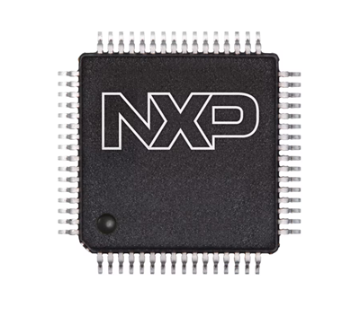
Figure 1. LPC84x Microcontroller
Overview of LPC84x Startup Power Issues
LPC84x microcontrollers are widely used in embedded systems because they combine processing capability, memory, and peripherals in a compact and energy-efficient device. However, reliable operation depends heavily on a stable and well-controlled power-up process. During startup, issues such as unstable supply voltage, improper voltage ramp rate, or inconsistent reset conditions can affect how the microcontroller initializes. These conditions may prevent the device from reaching normal operation or delay system boot.
Features of LPC84x Microcontrollers
1. ARM Cortex-M0+ Core
The LPC84x series is built around the ARM Cortex-M0+ processor, which is optimized for low power consumption and efficient performance. This 32-bit core supports fast interrupt handling and deterministic execution, making it suitable for embedded applications. Its simple architecture allows to build compact firmware while maintaining reliable processing capabilities. The core also supports standard ARM development tools for easier programming and debugging.
2. Embedded Flash Memory
These microcontrollers include on-chip flash memory used to store program code and firmware. The internal flash typically provides sufficient space for embedded applications without requiring external memory devices. Integrated flash allows faster access to instructions and improves overall system efficiency. It also simplifies hardware design because the microcontroller can operate independently after programming.
3. SRAM Memory
The LPC84x family integrates internal SRAM for runtime data storage and stack operations. This memory allows quick access for variables, buffers, and temporary processing data. Fast SRAM improves execution speed because the CPU can access data without waiting for external memory. It also supports multitasking operations within embedded applications.
4. Flexible Serial Communication Interfaces
Multiple communication peripherals are available for connecting external devices and modules. These include UART interfaces for serial communication, SPI interfaces for high-speed peripheral communication, and I²C interfaces for sensor and control networks. These built-in communication blocks simplify hardware integration in embedded designs. It can be used to connect displays, sensors, memory devices, and other digital components.
5. Analog Peripheral Support
The LPC84x microcontrollers include integrated analog features such as a 12-bit Analog-to-Digital Converter (ADC). This allows the device to measure analog signals from sensors or external circuits. Some variants also include Digital-to-Analog Converter (DAC) functionality for generating analog outputs. These capabilities enable the microcontroller to interface directly with signals.
6. Flexible I/O Configuration
General-purpose input/output (GPIO) pins allow the microcontroller to interact with external hardware components. The LPC84x includes flexible pin configuration features that allow multiple functions to be assigned to a single pin. This flexibility helps optimize PCB layouts and maximize available peripherals. GPIO pins can be configured for digital input, output, or alternate peripheral functions.
7. Low-Power Operation Modes
Low-power modes are included to reduce energy consumption in battery-powered applications. These modes allow the microcontroller to disable unused peripherals or reduce system clock frequency during idle periods. Power management features help extend battery life in portable devices. The system can quickly return to active operation when required.
8. Integrated Timer and Control Modules
Various timer modules are integrated to support time measurement, signal generation, and event control. These include multi-rate timers, state configurable timers, and watchdog timers. Timers enable precise timing control in embedded systems such as motor control, communication timing, or periodic task scheduling. These modules improve system reliability and performance.
LPC84x Block Diagram Overview
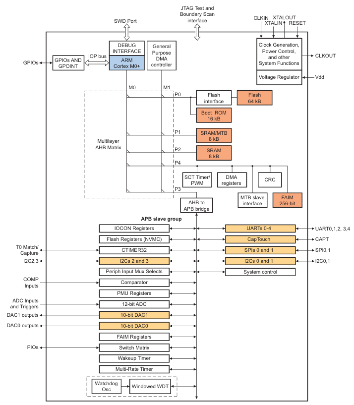
Figure 2. LPC84x Microcontroller Block Diagram
The LPC84x architecture integrates multiple functional blocks that work together to perform embedded processing tasks. At the center of the system is the ARM Cortex-M0+ CPU, which executes program instructions stored in internal flash memory while accessing data from SRAM. A multilayer AHB bus matrix connects the processor with memory modules and peripheral interfaces, enabling efficient communication between internal components. Clock generation and power management blocks control system timing and ensure stable device operation across different performance modes. Debug interfaces such as SWD allow to program and test firmware during development. Various peripherals, including timers, communication modules, and analog interfaces, are connected through the internal bus system to provide external device interaction. Together, these blocks form a compact microcontroller architecture designed for efficient embedded control.
LPC84x Power Supply Requirements
|
Parameter |
Symbol |
Typical / Range |
|
Supply Voltage |
VDD |
1.8 V – 3.6 V |
|
Analog Supply Voltage |
VDDA |
1.8 V – 3.6 V |
|
Operating Voltage (Typical) |
VDD |
3.3 V |
|
Power-On Voltage Threshold |
VPOR |
~1.5 V (typical) |
|
Brown-Out Voltage Level |
VBOR |
Configurable (~1.7–2.7 V) |
|
Active Mode Current |
IDD |
Device dependent |
|
Deep-Sleep Current |
IDD(DS) |
Very low (µA range) |
|
Maximum GPIO Voltage |
VIO |
Up to VDD |
|
Operating Temperature Range |
TA |
−40°C to +105°C |
|
Recommended Decoupling Capacitor |
— |
0.1 µF near each VDD pin |
LPC84x Reset Sources and Startup Behavior
Power-On Reset (POR)
Power-On Reset (POR) is an internal reset mechanism that activates automatically when power is first applied to the LPC84x microcontroller. Its main purpose is to hold the system in a reset state until the supply voltage reaches a safe operating level. When the device powers up, the POR circuit monitors the supply voltage and prevents the CPU from executing instructions prematurely. Once the voltage becomes stable, the reset condition is released and the processor begins executing code from internal flash memory. This ensures that the microcontroller always starts in a predictable state after power is applied. In the internal architecture, the reset system interacts with the clock and power management blocks before normal operation begins. This mechanism forms the foundation of the LPC84x startup process.
Brown-Out Reset (BOR)
Brown-Out Reset (BOR) is a protection mechanism that resets the LPC84x microcontroller when the supply voltage drops below a safe operating threshold. Its purpose is to prevent the CPU from operating under unstable voltage conditions that could cause unpredictable behavior. When the voltage falls below the configured level, the BOR circuit triggers a system reset to protect memory and peripheral states. After the supply voltage returns to a stable level, the device restarts normally. This feature helps maintain reliable operation in systems where power fluctuations may occur. In the internal architecture, voltage monitoring circuits work alongside the power control block to detect low-voltage conditions. As a result, the microcontroller can recover safely from temporary voltage drops.
External Reset Pin (RESET)
The external RESET pin provides a hardware method for resetting the LPC84x microcontroller from outside the chip. It allows external devices or control signals to force the microcontroller into a reset state when needed. When the RESET signal becomes active, the processor stops executing instructions and returns to the initial startup condition. This ensures that the system can restart cleanly during certain operational events. After the reset signal is released, the device performs its internal initialization process before running firmware again. External reset control is often used during programming, debugging, or system supervision. Within the internal system structure, this reset path connects directly to the central reset controller.
Watchdog Reset
A watchdog reset occurs when the watchdog timer detects that the system software is no longer operating correctly. The watchdog timer continuously monitors program execution by requiring periodic updates from the running firmware. If the software fails to refresh the timer within the expected period, the timer expires and triggers a system reset. This mechanism protects the system from software crashes, infinite loops, or unexpected firmware faults. After the reset occurs, the microcontroller restarts and begins executing the program again. In the internal architecture, the watchdog timer operates alongside system control logic and timers. Its purpose is to improve overall system reliability and maintain continuous operation in embedded systems.
LPC84x Power-Up Sequence
1. Power Supply Stabilization
When voltage is first applied to the device, the internal circuits require a short period for the supply voltage to stabilize. During this stage, the internal regulators and power management blocks establish proper voltage levels for the CPU and peripherals. The microcontroller remains inactive while this stabilization occurs. This prevents unreliable behavior during the early power-up stage. Stable voltage ensures that internal logic circuits can operate correctly.
2. Power-On Reset Activation
After the supply begins to stabilize, the Power-On Reset circuit keeps the processor in a reset state. This reset prevents the CPU from executing instructions until the voltage reaches a safe level. The reset controller monitors the supply voltage continuously during this stage. Only when the voltage exceeds the required threshold does the reset begin to release. This guarantees that the microcontroller starts with a clean system state.
3. Internal Clock Initialization
Once reset conditions are cleared, the microcontroller initializes its internal clock system. The clock generator starts the internal oscillator, which provides timing for CPU and peripheral operations. This clock becomes the main timing reference for system execution. The processor cannot run instructions without a stable clock source. Therefore, clock initialization is an important stage of system startup.
4. Memory Initialization
During the next stage, the processor prepares internal memory structures used by the program. Flash memory provides the firmware instructions, while SRAM stores runtime data. The system also prepares the vector table used for interrupt handling. This memory setup allows the processor to correctly locate the program entry point. Proper memory initialization ensures smooth firmware execution.
5. Peripheral Initialization
After memory preparation, the system enables important internal peripherals. These peripherals may include timers, communication modules, and control registers required by the firmware. Some peripherals remain disabled until the application software activates them. The initialization stage ensures that the basic system environment is ready. This step prepares the device for application execution.
6. Firmware Execution Begins
Once all internal initialization steps are complete, the processor begins executing the firmware stored in flash memory. Execution typically starts from the reset vector defined in the program code. From this point, the embedded application controls system operation. The firmware configures peripherals, processes input signals, and performs system tasks. This marks the transition from hardware startup to application runtime.
Common LPC84x Startup Power Issues
• Slow Voltage Ramp During Power-Up
If the supply voltage rises too slowly, the internal reset circuits may behave unpredictably. A slow ramp rate can delay proper reset release and affect device initialization. In some systems, the CPU may attempt to start before voltage is fully stable. This can result in inconsistent startup behavior.
• Power Supply Noise or Instability
Electrical noise on the power supply line can interfere with stable microcontroller startup. Noise may cause temporary voltage dips that trigger unintended resets. These fluctuations can affect internal clock and logic circuits. As a result, the microcontroller may restart repeatedly.
• Insufficient Decoupling Capacitors
Poor decoupling near the microcontroller power pins can cause unstable voltage during startup. Rapid current changes inside the chip require nearby capacitors to stabilize the supply. Without proper decoupling, voltage spikes may occur. This instability can affect system initialization.
• Voltage Drops During Startup
If the power supply cannot provide sufficient current at startup, the voltage may briefly drop. This situation can trigger brown-out reset conditions. Such drops may occur when other components in the system start simultaneously. These temporary dips can interrupt the boot process.
• Reset Signal Instability
External reset signals that fluctuate during power-up may cause repeated resets. If the reset signal does not remain stable, the microcontroller may never complete its initialization. This can prevent firmware from executing normally. Stable reset conditions are required for reliable startup.
• Improper Clock Source Availability
If the system relies on an external clock source that does not start correctly, the CPU may fail to run properly. Without a stable clock signal, instruction execution cannot begin. This may result in the system appearing unresponsive. Clock stability is important for normal microcontroller startup.
Troubleshooting LPC84x Startup Problems
• Verify the Supply Voltage Stability
The first troubleshooting step is measuring the microcontroller supply voltage using an oscilloscope or multimeter. The voltage should remain within the recommended operating range during startup. Any sudden drops or spikes may indicate power supply instability. Observing the voltage waveform during power-up can reveal hidden issues. Stable voltage is important for reliable microcontroller initialization.
• Check Reset Signal Timing
The reset signal should remain stable and properly synchronized with the power-up process. Many often monitor the reset pin to confirm that it behaves as expected during startup. An unstable or noisy reset signal may repeatedly restart the system. Verifying reset timing ensures that initialization occurs only after power becomes stable. Correct reset behavior supports proper system boot.
• Inspect Power Supply Filtering
Power filtering components such as decoupling capacitors should be examined carefully. These capacitors help maintain stable voltage during rapid current changes. Poor placement or insufficient capacitance may allow voltage noise to affect the microcontroller. Ensuring proper filtering improves startup reliability. Hardware inspection can often reveal missing or incorrectly placed capacitors.
• Confirm Clock Source Operation
The system clock must start correctly for the processor to execute instructions. Check oscillator signals to confirm proper operation. If the clock source fails to start, the CPU cannot run firmware. Monitoring the clock signal helps determine whether timing circuits are functioning correctly. Reliable clock operation is required for normal startup.
• Examine Firmware Initialization Code
Startup code inside the firmware may affect system initialization behavior. Review the reset handler and system initialization routines. Incorrect configuration of system registers or peripherals may delay normal operation. Verifying the startup code ensures that firmware initializes hardware correctly. Software inspection complements hardware debugging.
• Observe Startup Behavior with Debug Tools
Debug interfaces such as SWD allow to monitor processor activity during startup. Using debugging tools, check whether the CPU reaches the main program entry point. Breakpoints and debugging logs help reveal where initialization stops. This method provides valuable insight into system behavior during early startup stages.
Conclusion
Reliable startup of an LPC84x microcontroller depends on stable power, correct reset behavior, and a properly working clock system. Important startup stages include power stabilization, reset release, clock setup, memory preparation, and firmware execution. Problems such as voltage drops, noise, poor decoupling, or unstable reset signals can interrupt this process. Careful power design and systematic troubleshooting help ensure consistent startup and stable system operation.
About us
ALLELCO LIMITED
Read more
Quick inquiry
Please send an inquiry, we will respond immediately.
Frequently Asked Questions [FAQ]
1. What is the LPC84x microcontroller used for?
The LPC84x microcontroller is commonly used in embedded systems that require low power consumption and compact hardware. Typical applications include industrial control systems, sensor interfaces, consumer electronics, and IoT devices.
2. What development tools can be used to program LPC84x microcontrollers?
You can program LPC84x devices using ARM-compatible tools such as Keil MDK, MCUXpresso IDE, or IAR Embedded Workbench. These environments support debugging, compiling, and firmware development.
3. Does the LPC84x microcontroller require an external crystal oscillator?
No, the LPC84x includes an internal oscillator that can generate the system clock. However, some applications may use an external crystal for higher timing accuracy.
4. What is the maximum clock speed of LPC84x microcontrollers?
Most LPC84x devices operate at clock speeds up to about 30 MHz. This speed allows efficient processing while maintaining low power consumption.
5. Can LPC84x microcontrollers be used in battery-powered devices?
Yes, LPC84x devices are designed with multiple low-power modes that reduce energy consumption during idle periods. This makes them suitable for portable electronics, IoT nodes, and battery-powered embedded systems.

What Is an H7 Battery? Size, Features, and Vehicle Uses
on March 10th
Understanding DVI Connectors: Everything You Need to Know
on March 9th
Popular Posts
-

Complex Instruction Set Computers: How They Changed Computing?
on April 18th 147760
-

USB-C Pinout and Features
on April 18th 111967
-

Using Xilinx Unified Simulation Primitives: A Comprehensive Guide to FPGA Design and Simulation
on April 18th 111351
-

Power Supply Voltages in Electronics: Meaning of VCC, VDD, VEE, VSS, and GND
on April 18th 83729
-

RJ45 Connector Guide: Pinout, Wiring, Cable Types, and Uses
on January 1th 79516
-

The Ultimate Guide to Wire Color Codes in Modern Electrical Systems
The way our electrical systems use colors isn’t just for looks. Each wire color now indicates a specific function, making it easier to identify and handle electrical components correctly during ins...on January 1th 66930
-

Purge Valve Guide: Function, Symptoms, Testing, and Replacement for Optimal Engine Performance
The purge valve is a key part of a car’s system that helps keep the air clean by managing fuel vapors before they can escape into the atmosphere. This not only helps the environment by reducing pol...on January 1th 63079
-

Quality (Q) Factor: Equations and Applications
The quality factor, or 'Q', is important when checking how well inductors and resonators work in electronic systems that use radio frequencies (RF). 'Q' measures how well a circuit minimizes energy...on January 1th 63023
-

Achieving Peak Performance with the Maximum Power Transfer Theorem
The Maximum Power Transfer Theorem explains how energy from a source, such as a battery or generator, flows to a connected load. It shows the exact condition where the load receives the most power....on January 1th 54088
-

A23 Battery Specifications and Compatibility
The A23 battery is a small, cylinder-shaped battery with high voltage. Also called 23A, 23AE, or MN21, it runs at 12 volts and much higher than AA or AAA batteries. Its special design make...on January 1th 52160
HOT Part Number
-

IS25LQ025B-JNLE
ISSI, Integrated Silicon Solution Inc
IC FLASH 256KBIT SPI/QUAD 8SOIC
AD9764ARZ
Analog Devices Inc.
IC DAC 14BIT A-OUT 28SOIC
VI-711384B
Vicor Corporation
T 50/140/ 80 24V/ 3.1A
XRT83SL314IB
MaxLinear, Inc.
IC TELECOM INTERFACE 304TBGA
C152C
Powerex Inc.
SCR 300V 70A TO83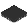
MC68882CRC25A
Freescale Semiconductor
MATH COPROCESSOR, 32-BIT
EPF81500ARC304-2
Intel
IC FPGA 208 I/O 304RQFP
FDC6332L
Fairchild Semiconductor
BUFFER/INVERTER PERIPHL DRIVER
74AHC1G125DBVRG4
Texas Instruments
IC BUF NON-INVERT 5.5V SOT23-5
ZXTN25040DZTA
Diodes Incorporated
TRANS NPN 40V 5A SOT89-3
LT1399CS#PBF
Analog Devices Inc.
IC OPAMP CFA 3 CIRCUIT 16SO
LT1963ES8-1.8#TRPBF
Analog Devices Inc.
IC REG LINEAR 1.8V 1.5A 8SOIC
EMK325BJ226KM-T
Taiyo Yuden
CAP CER 22UF 16V X5R 1210
THGAF8G9T43BAIR
Kioxia America, Inc.
IC FLASH 64GBIT UFS 153VFBGA
NVMFS5C410NWFAFT1G
onsemi
MOSFET N-CH 40V 46A/300A 5DFN
GRM188R61E225KA12D
Murata Electronics
CAP CER 2.2UF 25V X5R 0603
LTC488ISW#PBF
Analog Devices Inc.
IC RECEIVER 0/4 16SOIC
400BXW68MEFR18X20
Rubycon
CAP ALUM 68UF 20% 400V RADIAL -

IRF3805STRL-7PP
Infineon Technologies
MOSFET N-CH 55V 160A D2PAK
MAX365CSE+T
Analog Devices Inc./Maxim Integrated
IC SWITCH SPST-NOX4 85OHM 16SOIC
B82789C0513H002
EPCOS - TDK Electronics
CMC 51UH 250MA 2LN SMD AEC-Q200
AT24C128BY6-YH-T
Microchip Technology
IC EEPROM 128KBIT I2C 8MINI MAP
1.5SMC33A
Good-Ark Semiconductor
TVS, UNI-DIR, 1500W, 33V, DO-214
TPS2014P
Texas Instruments
IC PWR SWITCH N-CHANNEL 1:1 8DIP
AIAC-1812-39NJ-T
Abracon LLC
FIXED IND 39NH 2.8A 5.6 MOHM SMD
C3225Y5V1C226Z/1.30
TDK Corporation
CAP CER 22UF 16V Y5V 1210
MAX15012AASA+
Analog Devices Inc./Maxim Integrated
IC GATE DRVR HALF-BRIDGE 8SOIC
S25FL512SDSMFBG10
Infineon Technologies
IC FLASH 512MBIT SPI/QUAD 16SOIC
RCLAMP1851Y.TFT
Semtech Corporation
TVS DIODE 18VWM 12V SLP0603P2X3E
A3280LLHLT-T
Allegro MicroSystems
MAGNETIC SWITCH LATCH SOT23W
LMF100CIWMX
Texas Instruments
IC FILTER 100KHZ SWITCH 20SOIC
AT49BV1614-11TI
Microchip Technology
IC FLASH 16MBIT PARALLEL 48TSOP
C1608X6S1A685K080AC
TDK Corporation
CAP CER 6.8UF 10V X6S 0603
DIT4096IPWR
Texas Instruments
IC LINE DRIVER 28TSSOP
74404041470
Würth Elektronik
FIXED IND 47UH 560MA 987MOHM SMD
GRM0335C1E680JD01D
Murata Electronics
CAP CER 68PF 25V C0G/NP0 0201 -

1N2130A
Solid State Inc.
DIODE GEN PURP 150V 70A DO5
P5021NXN7TMC
NXP USA Inc.
IC SOC 64BIT 2X1.8GHZ 1295FCBGA
SG3543N
Microchip Technology
IC POWER SUPPLY SUPERVISOR 16DIP
AD633ANZ
Analog Devices Inc.
IC ANALOG MULTIPLIER 8-DIP
BLM15PX221SN1D
Murata Electronics
FERRITE BEAD 220 OHM 0402 1LN
RC4558DGKR
Texas Instruments
IC OPAMP GP 2 CIRCUIT 8VSSOP
MPC8308CVMAFD
Freescale Semiconductor
MPU, 32-BIT, 266MHZ, PBGA473
SN75374N
Texas Instruments
IC GATE DRVR LOW-SIDE 16DIP
BQ20Z90DBTR
Texas Instruments
IC GAS GAUGE FOR BQ29330 30TSSOP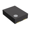
RP101K332D-TR
Nisshinbo Micro Devices Inc.
IC REG LIN 3.3V 300MA DFN1612-4B
HD64F3687HV
Renesas Electronics America Inc
IC MCU 16BIT 56KB FLASH 64QFP
2225SA332JAT1A\SB
KYOCERA AVX
CAP CER 3300PF 1.5KV NP0 2225
ST8034TDT
STMicroelectronics
IC INTERFACE SPECIALIZED 16SO
SRU1048-150Y
Bourns Inc.
FIXED IND 15UH 3.2A 29 MOHM SMD
MIC5213-3.6YC5-TR
Microchip Technology
IC REG LINEAR 3.6V 80MA SC70-5
MC34932EK
NXP USA Inc.
IC BRIDGE DRIVER PAR 54SOIC
TVP5146M2PFP
Texas Instruments
IC DIGITL VIDEO DECODER 80-HTQFP
BZX79C11
onsemi
DIODE ZENER 11V 500MW DO35