XC2S100E-6FTG256C FPGA Guide: Specifications, Features, and Applications
This guide explores the XC2S100E-6FTG256C, a cost-effective and versatile FPGA designed for embedded systems, industrial control, and digital logic applications. With a rich combination of logic cells, block and distributed RAM, and high I/O flexibility, it serves as a dependable solution for both modern applications and legacy system support. In this guide, you’ll learn what this FPGA can do, how it’s built, how to use it, and why it's still a good choice today.Catalog
XC2S100E-6FTG256C Overview
The XC2S100E-6FTG256C is a high-performance, low-cost FPGA from Spartan-IIE family, tailored for embedded systems, industrial automation, and legacy digital processing designs. With a capacity of 100,000 system gates and 2,700 logic cells, this device supports versatile logic applications while maintaining efficient power consumption through its 1.8V core. It incorporates 40 Kbits of block RAM and 38,400 bits of distributed RAM, which offers designers flexible memory configurations. Operating at speeds up to 275 MHz, it supports rapid data processing for time-critical tasks. Designed using 0.15 µm CMOS technology, the -6 speed grade indicates a reliable performance tier suitable for most mainstream applications. The Spartan-IIE family, which includes the XC2S100E-6FTG256C, ranges in logic density from 50K to 600K gates and features needed tools like four DLLs for advanced clock control, dedicated carry logic for arithmetic functions, and compatibility with 3.3V PCI/CardBus interfaces.
If you're looking for reliable FPGA solutions, the XC2S100E-6FTG256C is a solid choice, feel free to place your bulk orders with us anytime
XC2S100E-6FTG256C Features
Logic Capacity: The XC2S100E-6FTG256C offers 100,000 system gates, providing sufficient logic for moderately complex digital designs. Its 2,700 logic cells serve as the core configurable logic blocks that enable a wide variety of user-defined functions.
Embedded Memory: This FPGA includes 40 Kbits of synchronous block RAM, suitable for buffering, temporary data storage, or implementing FIFOs and other memory structures within the logic design.
Distributed RAM: In addition to block RAM, it offers 38,400 bits of distributed RAM that can be used for compact memory elements spread across the logic fabric. This is useful for implementing small lookup tables or configuration data close to processing logic.
User I/O Pins: The device provides up to 176 general-purpose I/O pins, allowing it to interface with a wide range of peripherals, external memory devices, or other ICs in the system.
High Operating Frequency: With a maximum internal clock rate of 275 MHz, the XC2S100E enables fast signal processing and supports high-speed operations necessary in control systems, communications, and signal acquisition.
Core Voltage: Operating with a core voltage of 1.8V, the device is designed for low power consumption while still maintaining sufficient performance for mid-range applications.
Process Technology: Manufactured using a 0.15-micron CMOS process, this device balances integration density with thermal efficiency and provides stable operation under industrial conditions.
Speed Grade: The “-6” speed grade denotes the standard performance variant within the Spartan-IIE series. It offers a balanced combination of speed and power efficiency suitable for a broad range of digital designs.
XC2S100E-6FTG256C Block Diagram
Input/Output Block (IOB)
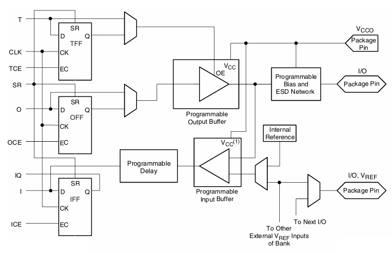
This diagram shows how the XC2S100E-6FTG256C FPGA handles signals going in and out of its I/O pins. The Input/Output Block (IOB) lets you control when and how data moves between the FPGA and the outside world. It has separate sections for input, output, and control logic. On the output side, signals come from flip-flops (TFF and OFF), which store the data. These are controlled by a clock (CLK), enable signals (TCE, OCE), and a set/reset input (SR). The output data goes through a programmable buffer that drives the signal out to the pin. This buffer can be tuned for strength and speed and includes protection against static electricity (ESD). For inputs, signals from the pin pass through a delay block and then a programmable input buffer. This buffer can adjust how it reads the signal, depending on voltage levels and standards. A reference voltage (VREF) helps it decide how to process the input, especially when using certain signal types.
Slave Parallel Mode
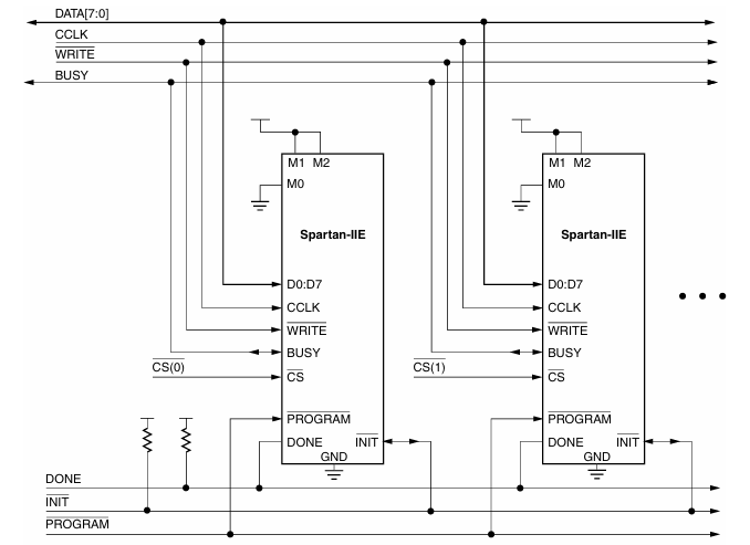
The diagram illustrates the Slave Parallel Mode configuration for multiple XC2S100E-6FTG256C Spartan-IIE FPGAs from AMD Xilinx. In this setup, several FPGAs are programmed simultaneously using a shared 8-bit data bus (DATA[7:0]), a common configuration clock (CCLK), and control signals such as WRITE and PROGRAM. Each FPGA receives the configuration data in parallel, allowing for faster programming compared to serial modes.
Each FPGA has its M0-M2 mode pins grounded, setting it into Slave Parallel mode, where the configuration data is pushed into the device by an external controller. The CS (Chip Select) line is used to enable individual devices, ensuring only one FPGA is active during configuration to avoid bus contention. The BUSY and DONE signals help monitor the status of each device during the process, while the INIT pin is shared to coordinate initialization across all devices. Pull-up resistors on DONE and INIT ensure proper logic levels when inactive.
XC2S100E-6FTG256C Specifications
|
Type |
Parameter |
|
Manufacturer |
AMD/Xilinx |
|
Series |
Spartan®-IIE |
|
Packaging |
Tray |
|
Part Status |
Obsolete |
|
Number of LABs/CLBs |
600 |
|
Number of Logic Elements/Cells |
2700 |
|
Total RAM Bits |
40960 |
|
Number of I/O |
182 |
|
Number of Gates |
100000 |
|
Voltage - Supply |
1.71V ~ 1.89V |
|
Mounting Type |
Surface Mount |
|
Operating Temperature |
0°C ~ 85°C (TJ) |
|
Package / Case |
256-LBGA |
|
Supplier Device Package |
256-FTBGA (17x17) |
|
Base Product Number |
XC2S100E |
XC2S100E-6FTG256C Applications
Industrial Automation and Control Systems
The XC2S100E-6FTG256C is ideal for implementing logic-intensive control schemes in industrial environments. It can manage signal processing, motor control loops, and programmable logic for robotics and manufacturing systems. Its fast I/O and reliable timing make it suited for interfacing with sensors, actuators, and supervisory controllers.
Embedded Systems and SoC Prototyping
This FPGA allows you to create custom embedded logic platforms and prototype System-on-Chip (SoC) architectures. With reprogrammable logic and distributed memory, it helps simulate processing cores, peripheral interfaces, and custom digital IP blocks quickly and affordably.
Automotive Electronics
The device can be used in vehicles for tasks such as managing digital dashboards, in-vehicle entertainment systems, and low-level signal processing in driver-assist systems. Its power efficiency and robust I/O support suit automotive-grade designs that require long-term dependability.
Educational and Training Platforms
With its approachable logic density and accessible toolchain (ISE Design Suite), the XC2S100E-6FTG256C is excellent for learning digital design, VHDL/Verilog programming, and system integration techniques.
Legacy System Maintenance and Upgrades
Many systems built in the early 2000s used Spartan-IIE FPGAs like this one. The XC2S100E-6FTG256C continues to be good for supporting and maintaining these systems, enabling repair or enhancement without full redesign, ensuring software and hardware compatibility.
XC2S100E-6FTG256C Similar Parts
The XC2S100E-6PQG208C is a member of the same Spartan-IIE family and offers the same logic capacity and performance specifications as the XC2S100E-6FTG256C, including 2,700 logic cells and 100,000 system gates. It is packaged in a 208-pin Plastic Quad Flat Pack (PQFP), making it suitable for designs that prefer or require leaded packages for easier inspection and rework. It is a strong alternative if you're transitioning away from BGA packaging and need a lower-cost or easier-to-solder footprint while maintaining full functional equivalency.
This part is virtually identical to the XC2S100E-6PQG208C, differing mainly in possible markings or sourcing, but still housed in the same 208-pin PQFP package. It retains the same -6 speed grade and electrical performance, making it a drop-in alternative in terms of logic behavior for designs already using the PQ208 footprint. This option is excellent when sourcing flexibility is needed, as it allows for compatibility with the same PCB layout while expanding your supplier options.
The XC2S100E-6FT256C shares the exact BGA pin count (256 balls) as the original XC2S100E-6FTG256C, although it may differ slightly in thermal or packaging specs (e.g., "FT" vs. "FTG"). Electrically and functionally, it’s nearly identical, and because it stays within the same BGA category and logic family, it’s the most direct replacement from a mechanical and performance standpoint. If you're looking for minimal PCB redesign, this part is likely the most seamless substitute.
XC2S100E-6FTG256C Programming Steps
1. Design Entry and Synthesis: To begin programming the XC2S100E-6FTG256C, you first need to create the digital logic design using a Hardware Description Language (HDL) such as VHDL or Verilog. This step is performed using the Xilinx ISE Design Suite or a similar synthesis tool. After writing the design, it is synthesized to convert the high-level logic into a gate-level netlist. The synthesis tool then generates a bitstream file (usually with a .bit extension), which contains the configuration data required to program the FPGA.
2. Select Configuration Mode: The Spartan-IIE family supports various configuration modes including Slave Serial, Master Serial, Slave Parallel, Master Parallel, and JTAG (Boundary Scan). You must select the mode that suits your system setup by correctly setting the mode pins (M0, M1, M2). These pins dictate how the FPGA will load its configuration data after power-up or reset. For example, JTAG mode is typically used for in-system debugging and flexibility during development.
3. Connect Programming Hardware: Depending on the configuration mode selected, connect the appropriate hardware. For JTAG programming, use a JTAG programmer like the Xilinx Platform Cable USB. This requires proper connections to the JTAG pins: TDI (Test Data In), TDO (Test Data Out), TCK (Test Clock), and TMS (Test Mode Select). Also, ensure the PROGRAM pin is wired to allow reinitialization. Proper grounding and VCC connections are important for stable operation during configuration.
4. Program the FPGA: Using the Xilinx iMPACT tool (from the ISE suite), load the .bit file to the FPGA. If using JTAG mode, iMPACT communicates with the FPGA via the JTAG interface. Internally, the process includes loading the CFG_IN instruction, shifting the bitstream through the Shift-DR state into the FPGA via TDI, and triggering configuration with the JSTART instruction. Once the bitstream is completely loaded, the FPGA moves into normal operation. Ensure the DONE pin goes high, indicating successful configuration.
5. Verify Configuration: After programming, it's important to confirm that the device has correctly received the configuration. The simplest check is observing the DONE pin, which should go high after a successful bitstream load. Additionally, the iMPACT software can perform a readback or verification process to compare the loaded bitstream with the original file, ensuring that no errors occurred during transmission.
XC2S100E-6FTG256C Advantages
Low Power Consumption
The XC2S100E-6FTG256C operates at a core voltage of just 1.8V, which reduces its power consumption compared to older FPGAs that run at 2.5V or higher. This makes it a preferred choice for battery-operated or thermally constrained systems, where managing heat and extending power efficiency are needed. The lower voltage not only improves energy efficiency but also helps in minimizing the size and cost of external power regulation components.
High I/O Count
This FPGA provides up to 182 I/O pins, offering a wide range of connection points for peripherals and system interfaces. This high pin count allows the XC2S100E-6FTG256C to handle complex signal routing and multiple external devices, such as memory interfaces, data buses, or communication modules. In systems that demand many parallel connections or mixed signal interfaces, this device reduces the need for additional multiplexing or external glue logic.
Enhanced Logic Resources
With 2,700 logic cells and a large number of configurable logic blocks (CLBs), this device gives ample resources for building sophisticated digital circuits. It supports moderate-to-complex designs, such as embedded controllers, custom data paths, and signal processing chains. Compared to earlier Spartan devices or CPLDs, this FPGA offers a noticeable improvement in logic density and design flexibility without escalating cost.
Integrated Block RAM
The XC2S100E-6FTG256C includes 40 Kbits of embedded block RAM, which allows to store temporary data, buffers, or lookup tables directly within the FPGA. This embedded memory reduces the need for external RAM chips, lowering BOM cost and improving data throughput. It’s useful for applications like data acquisition, buffering sensor inputs, or temporary data caching during processing.
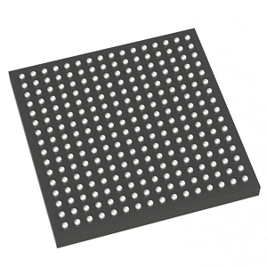
XC2S100E-6FTG256C Packaging Dimensions
• Package Type: 256-ball Fine-Pitch Thin Ball Grid Array (FTBGA)
• Body Size: 17 mm × 17 mm
• Ball Pitch: Typically 1.0 mm
• Mounting Type: Surface Mount
• Package Height: Approximately 1.4 mm
• Moisture Sensitivity Level (MSL): Yes, moisture sensitive
• Standard Packaging: Supplied in trays
XC2S100E-6FTG256C Manufacturer
The XC2S100E-6FTG256C is manufactured by AMD, following the acquisition of Xilinx, the original developer of the Spartan-IIE FPGA family. AMD, a global leader in high-performance computing and semiconductor technologies, now oversees the complete portfolio of Xilinx programmable logic devices, including legacy products like the XC2S100E-6FTG256C. This transition has strengthened AMD's presence in the FPGA and adaptive computing market, ensuring continued support and integration of Xilinx’s innovation heritage into AMD’s broader system-level solutions. While the XC2S100E-6FTG256C is officially classified as obsolete, AMD continues to facilitate lifecycle support, technical documentation, and migration resources for legacy designs built around Spartan-IIE devices.
Conclusion
The XC2S100E-6FTG256C is a powerful and low-cost FPGA that gives you 100,000 gates and 2,700 logic blocks to build custom digital functions. It has built-in memory, many input/output pins, and runs fast at up to 275 MHz. It uses only 1.8 volts, so it saves power. This chip is great for machines in factories, car systems, student projects, and fixing old designs. You can also choose other similar versions if you need a different package. Even though it’s not a new part, it still works well and is supported by AMD. It’s a smart pick for anyone building or fixing digital systems.
Datasheet PDF
XC2S100E-6FTG256C Datasheets:
Spartan, Virtex, XC17V00 24/Apr/2013.pdf
About us
ALLELCO LIMITED
Read more
Quick inquiry
Please send an inquiry, we will respond immediately.
Frequently Asked Questions [FAQ]
1. How does the XC2S100E-6FTG256C compare to newer FPGAs like Spartan-6 or Artix-7?
Compared to newer families, the XC2S100E-6FTG256C has fewer logic cells, lower memory capacity, and slower I/O. However, it's more cost-effective for simple or moderate applications, and its mature design makes it highly stable and well-documented.
2. What programming tools do I need for configuring the XC2S100E-6FTG256C?
You’ll need the Xilinx ISE Design Suite and a compatible programming cable such as the Xilinx Platform Cable USB. These tools allow you to create the bitstream and upload it via JTAG or other supported modes.
3. Can this FPGA handle both 3.3V and 2.5V I/O signaling?
Yes, the XC2S100E-6FTG256C supports a variety of I/O standards, including LVCMOS and LVTTL, and can be configured to operate with both 3.3V and 2.5V signaling through its IOB settings and VREF inputs.
4. What is the power consumption of the XC2S100E-6FTG256C under typical load?
Under typical load, the core power consumption is quite low due to its 1.8V core voltage. Exact power depends on the logic activity and clock frequency, but it is well-suited for thermally constrained systems.
5. Can multiple XC2S100E-6FTG256C devices be programmed at once?
Yes, using Slave Parallel mode, multiple devices can be configured simultaneously with a shared data bus. This speeds up production testing or system initialization in large-scale applications.
XCS30-3VQ100C FPGA: Features, Programming and Alternatives
on May 7th
AD8130AR Amplifier Guide: Features, Pinout, Applications and Datasheet
on May 6th
Popular Posts
-

Complex Instruction Set Computers: How They Changed Computing?
on April 18th 147778
-

USB-C Pinout and Features
on April 18th 112033
-

Using Xilinx Unified Simulation Primitives: A Comprehensive Guide to FPGA Design and Simulation
on April 18th 111352
-

Power Supply Voltages in Electronics: Meaning of VCC, VDD, VEE, VSS, and GND
on April 18th 83790
-

RJ45 Connector Guide: Pinout, Wiring, Cable Types, and Uses
on January 1th 79596
-

The Ultimate Guide to Wire Color Codes in Modern Electrical Systems
The way our electrical systems use colors isn’t just for looks. Each wire color now indicates a specific function, making it easier to identify and handle electrical components correctly during ins...on January 1th 66974
-

Purge Valve Guide: Function, Symptoms, Testing, and Replacement for Optimal Engine Performance
The purge valve is a key part of a car’s system that helps keep the air clean by managing fuel vapors before they can escape into the atmosphere. This not only helps the environment by reducing pol...on January 1th 63110
-

Quality (Q) Factor: Equations and Applications
The quality factor, or 'Q', is important when checking how well inductors and resonators work in electronic systems that use radio frequencies (RF). 'Q' measures how well a circuit minimizes energy...on January 1th 63043
-

Achieving Peak Performance with the Maximum Power Transfer Theorem
The Maximum Power Transfer Theorem explains how energy from a source, such as a battery or generator, flows to a connected load. It shows the exact condition where the load receives the most power....on January 1th 54097
-

A23 Battery Specifications and Compatibility
The A23 battery is a small, cylinder-shaped battery with high voltage. Also called 23A, 23AE, or MN21, it runs at 12 volts and much higher than AA or AAA batteries. Its special design make...on January 1th 52197
HOT Part Number
-

600S0R9BT250XT
American Technical Ceramics
CAP CER 0.9PF 250V C0G/NP0 0603
FMS7000MTC14X
Fairchild Semiconductor
FMS7000MTC14X
TLC6C598PWR
Texas Instruments
IC LED DRIVER PS 50MA 16TSSOP
FDMF6808N
onsemi
DRMOS MODULE
LTC2943IDD-1#PBF
Analog Devices Inc.
IC BATT MONITOR MULTI-CHEM 8DFN
B72650M0301K072
EPCOS - TDK Electronics
VARISTOR 470V 400A 2SMD JLEAD
C1005X6S0G154M050BB
TDK Corporation
CAP CER 0.15UF 4V X6S 0402
LTC1966IMS8#TRPBF
Analog Devices Inc.
IC RMS TO DC CONVERTER 8MSOP
TUSB320HAIRWBR
Texas Instruments
IC USB TYPE-C LOGIC/PORT 12X2QFN
LM1771UMM
Texas Instruments
SWITCHING CONTROLLER, VOLTAGE-MO
NCP3063PG
onsemi
IC REG BUCK BST ADJ 1.5A 8DIP
NCP161BFCT450T2G
onsemi
IC REG LINEAR 4.5V 450MA 4WLCSP
CY14B101P-SFXIT
Infineon Technologies
IC NVSRAM 1MBIT SPI 40MHZ 16SOIC
BZT52C18-E3-08
Vishay General Semiconductor - Diodes Division
DIODE ZENER 18V 410MW SOD123
LTM4624IY
Analog Devices Inc.
DC DC CONVERTER 0.6-5.5V 22W
NMR106C
Murata Power Solutions Inc.
DC DC CONVERTER 5V 1W
C0402X5R0G104M020BC
TDK Corporation
CAP CER 0.1UF 4V X5R 01005
AD7579JN
Analog Devices Inc.
IC ADC 10BIT SAR 24DIP -
LTV-702FM
Lite-On Inc.
OPTOISOLATR 5KV TRANSISTOR 6-DIP
GRM0225C1E1R7WA03L
Murata Electronics
CAP CER 1.7PF 25V C0G/NP0 01005
XCV400E-7PQ240I
AMD
IC FPGA 158 I/O 240QFP
BZT52C9V1
Diotec Semiconductor
DIODE ZENER 9.1V 500MW SOD123F
6-5353606-6
TE Connectivity AMP Connectors
CONN RCPT 220POS SMD GOLD
P0640Q12ALRP
Littelfuse Inc.
THYRISTOR 58V 150A 2TDFN
595D107X9016C2T
Vishay Sprague
CAP TANT 100UF 10% 16V 2812
1210AC562KAT1A
KYOCERA AVX
CAP CER 5600PF 1KV X7R 1210
C2012CH2A222J085AA
TDK Corporation
CAP CER 2200PF 100V CH 0805
MAX803SEXR+T
Analog Devices Inc./Maxim Integrated
IC SUPERVISOR 1 CHANNEL SC70-3
STF10NM60N
STMicroelectronics
MOSFET N-CH 600V 10A TO220FP
LT1963EST-3.3#TRPBF
Analog Devices Inc.
IC REG LINEAR 3.3V 1.5A SOT223-3
UMK105CK1R5CW-F
Taiyo Yuden
CAP CER 1.5PF 50V C0K 0402
170332-0012
Molex
Impact BP 4x18 85 Ohm Gl/
MCF5272VF66J
Freescale Semiconductor
IC MCU 32BIT 16KB ROM 196MAPBGA
VE-202-EY
Vicor Corporation
DC DC CONVERTER 15V 50W
LM258ADGKR
Texas Instruments
IC OPAMP GP 2 CIRCUIT 8VSSOP
5014610401
Molex
CONN FPC BOTTOM 4POS 0.5MM R/A -

TC427MJA
Microchip Technology
IC GATE DRVR LOW-SIDE 8CERDIP
EP20K400EBC652-2
Altera
IC FPGA 488 I/O 652BGA
SY100EP11UZI
Microchip Technology
IC CLK BUFFER 1:2 3GHZ 8SOIC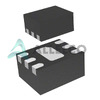
MAAM-011101-TR1000
MACOM Technology Solutions
IC RF AMP GPS 4GHZ-20GHZ 6TDFN
MC10H131MEL
onsemi
IC FF D-TYPE DUAL 1BIT 16SOEIAJ
SI5330F-B00214-GM
Skyworks Solutions Inc.
IC CLK BUFFER 1:8 200MHZ 24QFN
MAX8860EUA18+T
Analog Devices Inc./Maxim Integrated
IC REG LIN POS ADJ 300MA 8UMAX
CS5511-AS
Cirrus Logic Inc.
16-BIT DELTA SIGMA ADC
TL1014BF160QG
E-Switch
SWITCH TACTILE SPST-NO 0.05A 12V
06033C151JAT2A
KYOCERA AVX
CAP CER 150PF 25V X7R 0603
EMD4T2R
Rohm Semiconductor
TRANS NPN/PNP PREBIAS 0.15W EMT6
LM25011AMYX
Texas Instruments
IC REG BUCK ADJUSTABLE 2A 10MSOP
LM2733XMF
Texas Instruments
IC REG BOOST ADJ 1A SOT23-5
AM2917APC
Advanced Micro Devices
IC TXRX NON-INVERT 5.25V 20DIP
MAX3082CSA+T
Analog Devices Inc./Maxim Integrated
IC TRANSCEIVER HALF 1/1 8SOIC
FDMC86570L
onsemi
MOSFET N-CH 60V 18A/56A POWER33
XCR3256XL-10FT256I
AMD
IC CPLD 256MC 9.1NS 256FTBGA
FQP6N60C
Fairchild Semiconductor
POWER FIELD-EFFECT TRANSISTOR, 5